To overcome the beam squint in wide instantaneous frequency, we review a number of system-level optical controlled phase array antennas for beam forming. The optical delay network based on a fiber device in terms of topological structure of an N-bit optical switch, fiber grating, high-dispersion fiber, and vector-sum technology is discussed, respectively. Lastly, an integrated circuit is simply summarized.
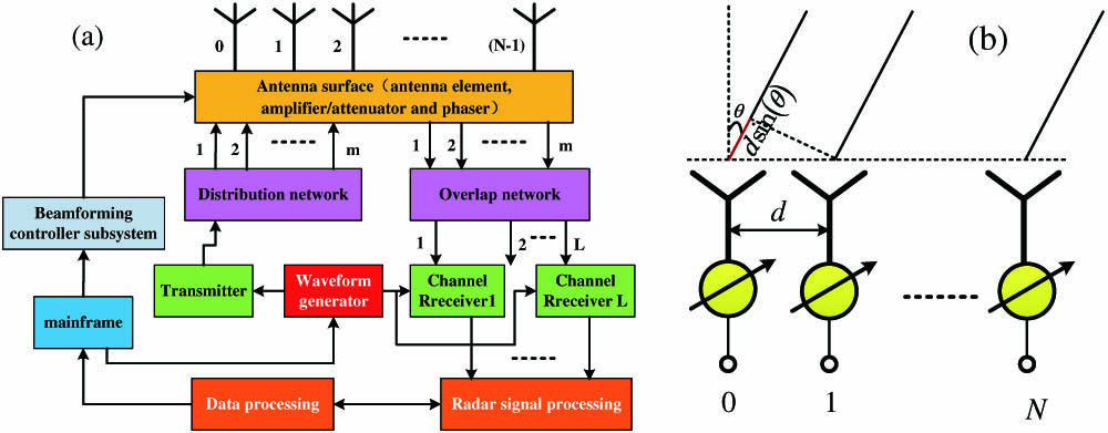
Radar is extensively used to detect space targets in civilian and military areas[1–6]. With the development of advanced technology, the researches paid extensive attention to the radar with ultra-distance and high resolution. However, due to the limitation of materials and power consumption, it is hard to increase the output power of a single transmitter. In order to overcome this difficulty, parallel coherent technology with multiple transmitters is used to enhance the received power. In this case, the increase of the antenna size largely increases the volume and weight of the radar. In addition, recent radar systems tend to be highly capacious and multifunctional, and cover more bands. A pattern reconfigurable antenna enables us to avoid noisy environments, maneuver away from electronic jamming, and save energy by redirecting the signal toward the intended users, which is frequently used to increase channel capacity and broaden the coverage area. Therefore, the phase array radar emerges in this movement[4]. Figure 1(a) shows the basic structure of the conventional phase array radar. The transmitter/receiver elements are uniformly laid out on the antenna surface to realize the ultra-large aperture called a phase array antenna (PAA). The microwave phase shifter and amplifier/attenuator are used to control the phase and magnitude of the microwave signal, respectively. The power distribution/overlap network is used for distribution and coherent combination.
Figure 1.(a) Schematic diagram of the phase array antenna. (b) Schematic diagram of beam forming using phase shifters.
Figure 1(b) shows the schematic diagram of a microwave PAA. It consists of antenna elements. The microwave signal is first through the phase unit to add the phase . So, the far field of the antenna beam at the angle is given by[4]where is the magnitude of the microwave signal in the antenna element; , where is the frequency of the microwave signal, is the distance between the adjacent antenna elements. When the pattern of each antenna element is isotropic, the antenna beam is proportional to the array factor of the antenna. If the beam is pointed to the angle , the addition phase is set as[4]where is the wave number of the microwave signal, and is the speed of light in vacuum. The microwave phase shifter provides a constant phase shift in a fixed frequency range. For a bandwidth signal, the additional phase is not proportional to the instantaneous frequency. Therefore, the undesirable shifting of the beam forms the angle of , which results in the decrease of the beam forming gain called the beam squint. The offset angle of the beam is written as[4]
To realize ultra-high resolution detection, a wide instantaneous bandwidth is needed in modern radar. Demand for broadband and narrow band in the phase array radar conflicts with each other. Therefore, a time shifter is considered as an alternative approach to achieve a wide instantaneous bandwidth. A true-time delay (TTD) line is introduced to compensate the path difference between the antenna elements. The time delay can be expressed as
Sign up for Chinese Optics Letters TOC. Get the latest issue of Chinese Optics Letters delivered right to you!Sign up now
For all frequencies, the addition phase is expressed as
When Eq. (5) is substituted into Eq. (1), Eq. (1) can be rewritten as
From Eq. (6), we can see that constructive interference in the direction angle can be obtained at all frequencies. Even if the instantaneous frequency is changed, the beam forming direction is still unchanged. Although the electronic integrated circuits (EICs) in recent years have made great progress, the approach suffers from bandwidth limitations and high insertion loss. To break such electronic bottleneck, photonic solutions with ultra-broad bandwidth and inherently low loss can overcome the beam squint both at the system level and integrated circuit level. Thanks to the inherent advantages brought by photonic technology, such as light weight, compactness, low cost, and anti-electromagnetic interference, it is of great interest to implement the beam forming network in the optical domain[1,2]. At the integrated circuit level, EICs can be combined with low loss photonic integrated circuits (PICs), where PICs are used for large delays, and EICs are used for sub-array delays. At the system level, fiber devices are the mainstream solution for photonic beam forming.
In this Letter, we review recent progress on photonic beam forming with emphasis on the system-level optical time delay network. Meanwhile, a novel approach based on vector-sum phase shifting is also reviewed. Lastly, the approach based on PICs is summarized.
Optical beam forming based on optical path switching[7–9] is a popular approach in the past decade. Dense wavelength division multiplexing (DWDM) or an optical switch is used to switch the optical path. Tacking the optical switch, for example, the delay lines are internally connected by 2 × 2 optical switches, which can be switched between the bar-state and cross-state by tuning the driving voltage. As the main component in the optical delay network, a number of optical switches can be used to realize path switching, such as the micro-electro mechanical switch (MEMS), thermo-optic switch, magneto-optic switch, and electro-optic switch. Therefore, various time delays are obtained by changing the optical transmission path. Although ultra-fast switching speed can be realized, the magnitude mismatch is a great challenge due to the optical path change in different time delays, which makes the figure of merit change with the direction of the desired main lobe[10]. Apparently, a smaller magnitude mismatch could boost the overall performance of switch-based optical beam forming.
Based on this technology, multi-channel, multi-bit programmable photonic beam forming is proposed as the structure shown in Fig. 2[9]. The laser array provides separated optical carriers with the wavelength on the information technology unit (ITU) grid. A Mach–Zehnder modulator (MZM) biased at is driven by a radio frequency (RF) signal. The modulated optical signal is amplified by an erbium-doped fiber amplifier (EDFA) and passes through optical splitter to transmit in the photonic TTD (PTTD) subnetwork. The delay subnetwork in Fig. 2(b)[9] is cascaded by MEMS. Each delay element can provide multi-bit TTD. After demultiplexing in the DWDM, the optical signal is separated and converted to an electrical signal at a photodetector (PD).
Figure 2.(a) Schematic of a multi-channel, multi-bit programmable photonic beam former. (b) Schematic of a delay subnetwork. DWDM, dense wavelength division multiplexing; MZM, Mach–Zehnder modulator; EDFA, erbium-doped fiber amplifier; PTTD, photonic true-time delay; PD, photodetector; MEMS, micro-electro mechanical switch.
The radiation pattern is demonstrated, where and at . The steering angles of the main lobe in Fig. 3[9] are 13.1˚, 29.9˚, −33.2˚, and −17.9˚, respectively. The theoretical results (black line) in Fig. 3[9] are well in agreement with the experimental results (red line). This technology offers the significant advantage of simple construction. Due to the different transmission paths in a different time delay, it is hard to compensate the phase and magnitude error between each channel. Meanwhile, the time delay lines based on the fiber grating (FG) are reported with the advantage of low cost, simple construction, and low complexity[11,12].
Figure 3.PAA radiation patterns based on photonic beam former.
Photonic beam forming based on the FG as the delay line is shown in Fig. 4(a)[11]. As the main component, the group of FGs is a fiber Bragg grating (FBG), chirped FG (CFG), or other kinds of FGs. A light wave from a tunable laser source (TLS) is modulated by an RF signal in the MZM and divided into N equal channels. The split optical signals are transmitted along the FGs and reflected from different positions. The optical signals are converted into electrical signals at the PDs. Figure 4(b)[11] shows the time delay results of nine channels at different wavelengths. It can be seen from Fig. 4(b)[11] that for a given wavelength , the time delay values change linearly with the wavelength. For a fixed wavelength, the time delay difference is constant between adjacent channels. With the FBGs as the time delay lines, multiple reflection regions are fabricated in one single-mode fiber (SMF), and the gap between adjacent reflection regions is kept equal. It becomes very different to fabricate the desired FBGs. The FGs are mainly limited by the phase ripples induced by the multiple reflections in the FGs.
Figure 4.(a) Beam forming based on FG. (b) The time delay curves of the nine channels. TLS, tunable laser source; PC, polarization controller; EOM, electro-optical modulator; FG, fiber grating; PD, photodetector.
The CFG[13–17] is an alternative device to replace the FBG as time delay line. As shown in Fig. 5(a)[16], N TLSs with wavelengths from to are modulated by an RF signal in the MZM after a power combiner. The modulated light signals are fed to the CFG and reflected at different positions. The PD converts the optical signal to an electrical signal after demultiplexing in wavelength division multiplexing (WDM). Figure 5(b)[16] shows the four-element time delay results. The experimental results show a very good agreement with the theoretical results. Using one CFG in the whole system is a clear advantage compared to the numerous FBGs that may result in inaccuracy due to the mismatches with each other. Besides, the RF power degradation of beam forming due to grating chromatic dispersion is accrued in high frequency. The FG technique is mainly limited by the phase ripples induced due to the multiple reflection positions.
Figure 5.(a) Beam forming based on CFG. (b) Time delay measurement results for four channels. TLS, tunable laser source; MZM, Mach–Zehnder modulator; WDM, wavelength division multiplexing; PD, photodetector.
The dispersion-based delay technique is considered a promising technique due to the compactness, low insertion loss and light weight[18–25]. The high-dispersion fiber, either the photonic crystal fiber (PCF)[18–21] or dispersion compensation fiber (DCF)[22–25] is usually a better choice than a conventional SMF, and it can reduce the overall length of the time delay line. The PCF-based time delay line with high-dispersion value can largely reduce the size and weight of the system. Because of the mode field mismatch, the maximum loss between the SMF and PCF is more than 10 dB, even in the special fusion joining process[18–21]. The DCF-based delay line is another excellent choice to realize the time delay with the advantage of high dispersion and low connection loss[22–25].
The schematic diagram of the DCF-based beam forming is shown in Fig. 6[24]. The optical carrier is emitted from a TLS with the wavelength from to . The amplified RF signal in the low noise amplifier (LNA) modulates the optical carrier in the MZM biased at . The modulated optical signal is amplified by an EDFA and divided equally into eight parallel light paths. The time delays are implemented by tuning the optical wavelength in the DCF-based time delay network. After correcting the phase and magnitude errors, the optical signals are converted into electrical signals at PDs.
The time delay is measured in Fig. 7(a)[24]. As can be seen from the measurement results, the time delay is linearly proportional to the optical wavelength for all of the channels, and the time delays are equal among eight channels at the wavelength of 1545 nm. The maximum time delay of two adjacent paths is 40.7 ps. The magnitude measurement results are shown in Fig. 7(b)[24]. The magnitude variations are within , and the magnitude among the eight paths is less than . The radiating patterns of the PAA are measured at different radio frequencies in the far field. The steering angle shown in Fig. 7(c)[24] can be scanned over in the direction normal to the antenna array facet, which agrees well with the theoretical curve (black line). From the measured results, we can see that the RF steering angle is changing with the optical wavelength, independent of the RF, where there is not a beam squint in the wide band.
Figure 7.(a) Time delays of the DCF-based TTD units. (b) Amplitude characteristics for eight paths through the TTD device. (c) Beam steered angles at different frequencies.
In order to verify the performance of the proposed optical PAA (OPAA), target detection in terms of the single-target and double-target ranging is carried out, respectively. For single-target detection, the wavelength is set as 1545 nm, and the chirped frequency is 8–12 GHz. Firstly, the system delay is calibrated as a reference to zero delay. Then, it is placed at 1.25, 1.65, 2.95, and 3.95 m from the transceiver with the transmitting/receiving antennas side to side. With normalized cross-correlation operation, the compressed microwave pulses are shown in Fig. 8[24]. The initial length of the time delay line (blue line) is 268.412 m. Therefore, the calculated round-trip target ranging is 2.485, 3.277, 5.881, and 7.891 m. From the experimental results, the measurement error is less than 1.5 cm, which resulted from the range error. To demonstrate the range resolution, double-plates are placed side by side, but separated by a distance along the range direction. The separated distances between the double plates are 1.9, 3.2, 4.5, and 6.0 cm. After cross-correlation, the normalized experimental results are shown in Figs. 9(a)–9(d)[24]. The round-trip distances of the double target are 0, 3.8, 5.0, and 7.6 cm, respectively. From the measurement result, the range resolution of matches well with the theory result of .
As we all know in the DCF-based PAA, the wavelength determines the time delay in the optical delay network. So, the wavelength switching speed determines the beam scanning time. For a commercial TLS, the wavelength switching time is normally at a level of milliseconds. The beam scanning time limits the application field of the DCF-based phased array radar. Therefore, a DCF-based PAA using an ultra-fast wavelength-swept laser source is proposed[25]. The schematic architecture of the proposed fast-swept DCF-based PAA system is shown in Fig. 10(a)[25].
Figure 9.(a)–(d) Measurement result for the double target.
The commercial TLS is replaced by the proposed ultra-fast wavelength-swept laser source shown in the black dashed box in Fig. 10(a). It consists of a multi-wavelength laser (MWL), a polarization controller (PC), an arbitrary waveform generator (AWG), an LNA, and a length of DCF. The wavelength from to with a fixed wavelength spacing of is sent to the MZM via a PC. The multi-wavelength light is truncated into an optical pulse at the output of the MZM, which is driven by a square pulse, as shown in Fig. 10(b). The time-gated optical signal is then dispersed by a length of DCF to realize temporary stretch, as shown in Fig. 10(c). The time interval between two adjacent wavelengths after dispersion is expressed as , where D is the dispersion coefficient, is the length of DCF, and represents the wavelength spacing. In order to realize wavelength sweeping without spectrum overlap, time duration and period should meet the following conditions:
When the conditions can be satisfied, we can implement a continuously wavelength-swept laser source. The wavelength sweep range is freely tuned by adjusting the spectrum of the MWL, time gate, and dispersion. The measured spectrum of a six-channel laser source with = 2.4 nm ranging from 1546 to 1558 nm is shown in Fig. 11(a)[25]. The waveform of the electrical pulse is shown in Fig. 11(b)[25] with a time duration of 2.04 ns. The received signals, as shown in Fig. 11(c)[25], have a scan periodicity about 12.48 ns with a duration time of 2.08 ns, which means the angle scan in the order of nanoseconds was achieved. Those improvements create more possibilities for the application of TTD-PAA systems in fast spatial detection.
Figure 11.(a) Measured spectrum. (b) The waveform of the electrical pulse. (c) The received signals of the PAA system with wavelength spacing of 2.4 nm.
Although optical TTD (OTTD) can realize a squint-free beam former, delay networks based on optical phase shifters are still widely used if the work bandwidth is not large. Beam forming based on vector-sum phase shifting is reported in Refs. [26–32]. In Ref. [26], the phase shifted optical signal is split into two paths with different fiber lengths by a variable directional coupler. By controlling the coupling ratio of the variable directional coupler, the combined signal after the PD has different phase shifts. The main limitation is that N independent sets of a laser source, modulator, and vector-sum module are required for N antenna elements, which is complex and costly. Besides, flexible beam forming technologies based on programmable photonic processors comprising a two-dimensional (2D) array of liquid crystal are also proposed in Ref. [28]. The magnitude and phase of the spectrum component can be operated independently. This approach can manipulate the phase and magnitude of different optical spectral components, but the antenna elements are limited by the number of the output ports of the programmable photonic processor (typically ). Pan’s group proposes beam forming based on single-sideband plus carrier () polarization modulation[31]. In the system, the polarization-modulated signal is split into N paths by the coupler, and each path includes one PC, one polarization beam splitter (PBS), and one PD. The PC together with the PBS serves as a polarizer. When the polarization direction of the polarizer is aligned with one principal axis of the polarization modulator, the phase of the generated microwave signal at the PD is 0°, and, if the polarizer is rotated to select the optical signal along the other polarization axis, this phase is changed to 90°. For other polarization directions, the phase shift is , where is the angle between the polarization direction of the polarizer and one principal axis of the polarization modulator. As a result, the phase shift can be independently and continuously tuned from to 180°. The phase shift can be changed by carefully adjusting the polarization of the PC before the PBS in each path. The stability of the system limited by the polarization state is hard to handle.
To reduce complexity and interconnection loss, integration of such devices[33–38] is the important trend for the future. OTTD networks for large aperture antennas arrays require delay lengths in the tens of nanoseconds scale. Several system-level fiber devices have been demonstrated, which are attractive due to their low loss, but suffer from the fact that they are bulky and must have their length precisely cleaved. As a result, integration of such devices would benefit the system by decreasing the footprint, increasing the delay accuracy and stability, and reducing the cost. Many fully integrated OTTDs have been reported[33–38]. Silicon-based waveguide technology is used to fabricate the N-bit delay line with the advantage of ultra-fast switching speeds up to gigahertz (GHz)[33]. High-propagation loss limits the cascaded series and the delay line length. - or -based TTD lines can realize longer delay lines and higher bit count delays due to the low propagation loss[35]. The optical switch is based on the thermo-optical effect, and the switching speed is only a few kilohertz (kHz). Hybrid integrated technology is considered as a promising approach to fabricate the N-bit delay line[38]. An InP-based optical switch and a -based delay line are connected by bonding technology to realize a fast switching, low loss, compact TTD line.
In this paper, OTTD for beam forming based on fiber devices is reviewed and explored. The most popular OTTD design is usually based on path section. The main issue is to balance the magnitude and the phase among different optical paths. The FGs as the TTD line were discussed, including the FBGs, CFGs, and other FGs. The time delay is simply changed by tuning the optical wavelength. The limitation based on the FGs is mainly the phase ripples induced by the multiple reflections in FGs. To overcome the problem, dispersion-based TTD technology is proposed to achieve the TTD. Since beam scanning time is determined by the wavelength switching speed, an ultra-fast wavelength-swept laser source is also reviewed, replacing the conventional TLS to increase the scanning speed. Meanwhile, beam forming is based on vector-sum technology. Moreover, on the integrated circuit level, the integration of beam forming can be considered as a long-term evolution trend.