
Jiaqi Zhu, He Zhu, Mengjuan Liu, Yao Wang, Hanlun Xu, Nasir Ali, Huiyong Deng, Zhiyong Tan, Juncheng Cao, Ning Dai, Huizhen Wu. Ultrabroadband and multiband infrared/terahertz photodetectors with high sensitivity[J]. Photonics Research, 2021, 9(11): 2167
- Photonics Research
- Vol. 9, Issue 11, 2167 (2021)
Abstract
1. INTRODUCTION
Infrared (IR) and terahertz (THz) detection technologies are highly desirable and intensively explored because of their indispensable applications in astronomical and civil fields [1–8]. The broadband response is insistently pursued by both of them to increase detecting capabilities and extend the application fields [1,2]. For instance, broadband detectors are crucial for the accurate measurement of the atmospheric spectra of carbon dioxide, water vapor, and other gases from space, which is a major concern for the climate and weather predictions [9–11]. Besides, multiband detection capability is one of the momentous goals pursued by advanced IR detection systems. Hence, enhanced target discrimination and identification with lower false-alarm rates can be achieved, which is greatly beneficial to target recognition, airborne surveillance, navigational aids, and so on [12–15]. It is a facile method to realize multiband IR detection in a sequential mode that combines broadband detectors with optical components such as lenses, prisms, and gratings [12]. Concerning THz detection, extending the response range is extremely promising in deep-space exploration, health care, security screening, national defense, nondestructive inspection, and so on [16–21].
IR and THz are contiguous in the electromagnetic spectrum, and there is a considerable application prospect to assemble IR and THz detections for the realization of ultrabroadband IR/THz detectors. Thermal detectors have the capability to cover such a broadband IR/THz region [22–25]. Unfortunately, these detectors deliver modest performance, such as low sensitivity and slow response speed, restricting their application spheres and values [2,26,27]. Blocked-impurity-band (BIB) detectors are a special type of extrinsic photon detectors with response wavebands commonly within 5–300 μm. Owing to their high sensitivity, low dark current, and broad response range, BIB detectors have been widely employed in astronomical applications [28–31]. The creative development of an ultrapure blocked layer (BL) between the absorbing layer (AL) and one of the two contact layers (CLs) makes it feasible to substantially dope the AL while dark current is deeply suppressed [32,33]. Hereby, an impurity band is formed, reducing the ionization energy of the dopants and thus broadening the response coverage. Recently, plentiful researches have been devoted to the development of BIB detectors, most of which were focused on sensitivity improvement [34–41]. However, the tremendous potential of BIB detectors to achieve ultrabroadband IR/THz detection is yet to be discovered.
In this work, phosphorus-doped germanium (Ge:P) BIB detectors are fabricated, where the AL is prepared using an ion implantation technique. Response spectrum measurements reveal that the detectors cover an ultrabroadband wavelength range with dual response wavebands in the IR and THz regions, respectively, which has not been covered by a single photon detector yet. Conventional BIB detectors cover a single waveband because only one impurity band is formed to absorb photons, but herein they are upgraded. Besides the P impurity for THz detection, two intrinsic defects generated during doping are also tactfully used for IR detection. Blackbody responses and dark current-voltage (I-V) characteristics were also measured sequentially, and the high sensitivity of the detectors is demonstrated. The detectors are highly significant in numerous applications.
Sign up for Photonics Research TOC. Get the latest issue of Photonics Research delivered right to you!Sign up now
2. EXPERIMENTAL PROCEDURE
The schematic of the device structure is shown in Fig. 1(a), including a high-purity Ge substrate, an AL, a BL, two CLs, and two electrodes. Since Ge:P is n-type, the electrode adjacent to the BL is positively biased when the detectors work [32]. A small density of acceptors in the original substrate is supposed to exist, and thus it also exists in the AL. All of the acceptors are compensated by the high-density P donors and are ionized in the AL [32]. Different from the acceptors with fixed sites, the ionized P donors are mobile due to the hopping conduction effect in the P impurity band [42]. With the positive bias applied, the ionized donors are swept out through the AL away from the AL/BL interface, leaving behind a depletion region as displayed in Fig. 1(a). Only the photogenerated carriers in the depletion region contribute to the response signal; thus, a longer depletion region will bring forth a stronger detector response [32]. The above is how conventional n-type BIB detectors work.
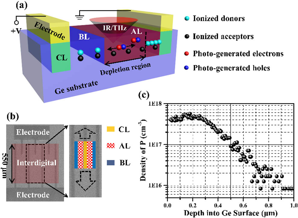
Figure 1.(a) Schematic for the Ge:P BIB detectors. (b) Partly false-color SEM image for a unit of the detectors; inset: two magnified interdigital cells. (c) The density profile of P atoms in the AL, which was obtained by SIMS measurement.
The fabrication of the Ge:P BIB detectors is simple and easy, where several micro-nano fabrication techniques were used. First, the AL and the CLs were developed in succession by implanting P ions into the high-purity Ge substrate with different doses in respective patterns. In this way, the BL was naturally developed by the substrate. Afterwards, a rapid thermal annealing technique was implemented at 700°C for 30 s to make Ge recrystallize and thus repair the implantation damage. Subsequently, an aluminum (Al) film was deposited using magnetron sputtering, followed by a lift-off technique to develop patterned electrodes. Before all patterned techniques were carried out, corresponding lithographies were utilized. Finally, the detectors were finished, having a planar structure similar to those reported previously [37–40,43]. Figure 1(b) presents a partly false-color scanning electron microscope (SEM) image of one of the detectors with six interdigital cells, and the inset shows two magnified interdigital cells where the distribution of the AL, BL, CL, and electrode is vivid. All of the fabricated detectors have the same interdigital structure, the same AL (or BL) width of 550 μm, and the same AL length of 40 μm, but different BL lengths. The detailed structural parameters of the detectors are presented in Table 1. Before the performance characterizations of the detectors, secondary ion mass spectroscopy (SIMS) of the AL was performed to obtain the detailed density distribution of P atoms as depicted in Fig. 1(c). With the depth into Ge surface below 0.3 μm, the P density is nearly within ; as long as the depth is below 0.5 μm, the donor density remains above . Structural Parameters of the Fabricated DetectorsNo. AL Length BL Length AL & BL Width #1 40 μm 25 μm 550 μm #2 21 μm #3 17 μm
To characterize the detectors, all of them were packaged and mounted into a continuous-flow liquid helium dewar with a sensitive temperature controller. The photoresponse spectra were measured using a Fourier transform infrared (FTIR) spectrometer (Bruker VERTEX 80v) with a vacuum cavity. The blackbody responses were measured utilizing a standard cavity blackbody at 1000 K (Infrared System, IR564/301). The measurement setups for the response spectra and the blackbody responses are displayed in the following section. The dark I-V characteristics were measured with a semiconductor parameter analyzer (Keithley 6517B) under dark condition. Without a specific statement, the above characterizations of the detectors were performed at 4.5 K.
3. RESULTS AND DISCUSSION
The measurement setup for the photoresponse spectra of the detectors includes a global illuminant, the FTIR spectrometer, a continuous-flow liquid helium (LHe) dewar with a sensitive temperature controller, and a low-noise current amplifier (SR570). The schematic of the measurement setup is shown in Fig. 2. The detectors are packaged and mounted in the dewar beforehand, which is then pumped into the vacuum by a pump I. LHe is used for refrigeration, ensuring that the operating temperature of the detectors is low enough. Since the dewar is a vacuum, no freezing occurs after the refrigeration. The dewar is connected with the temperature controller, such that the operating temperature is accurately adjustable. In order to eliminate the influence from air molecules, all space where light travels is sealed and pumped into the vacuum by pump II as shown in Fig. 2. The following is the measurement process. Light, including IR and THz wavebands, is emitted from the global illuminant and incident into the FTIR spectrometer, the emittance versus wavelength of which can be found in Ref. [44]. The spectrometer is controlled by a computer on which the spectroscopic software OPUS is installed. After release by the spectrometer, the light travels through the dewar window and is incident onto the detectors, and therein the electrical signals occur. Sequentially, the signals are amplified by the amplifier and then read out by the computer. In this way, the response spectra of the detectors are obtained. Since there is no beam splitter or window that could cover a consecutive wavelength range of 3–180 μm, two wavebands, 3–27 μm and 15–180 μm, are measured in succession by altering the beam splitters in the FTIR spectrometer and the windows on the dewar. The background spectra of the two wavebands (i.e., the photon-energy distributions of the respective measurement setups) are also measured with different standard detectors.
![]()
Figure 2.Schematic of the measurement setup for response spectra.
The method for obtaining an overall response spectrum is as follows. The response photocurrent spectra in the two wavebands are measured first, and then both of them are normalized by respective background spectra for background correction. Referred to the overlapped wavelength band of the two wavebands, an overall response spectrum is attained by stitching the two spectra. All response spectra thereinafter are acquired utilizing the above method. The overall response spectra of detectors #1 and #2 at 4.5 K are shown in Figs. 3(a) and 3(b), respectively. All of the spectra show ultrabroadband and multiband IR/THz responses. The IR and THz response bands range in 3–28 μm and 40–165 μm, with peaks at 16.3 μm and 116.5 μm, respectively. Although there are several valleys in the IR band, located at 9.5, 12.5, 19.0 μm, and so on, the coverage of this waveband is still extremely broad because these valleys are very narrow. Compared with common multiband IR detectors developed by such detecting systems as HgCdTe photodiodes, quantum-well IR photodetectors (QWIPs), quantum dot IR photodetectors (QDIPs), and type-II strained-layer superlattice (T2SLS) photodiodes, the coverage advantage for our detectors is evident [45–48]. Most of the abovementioned detectors are cut off at below 15 μm, and going after broader coverage badly reduces their sensitivity, increasing the production cost [49]. The THz response band of the detectors extends to a longer wavelength than unstressed gallium-doped Ge (Ge:Ga) BIB detectors, the most widespread Ge-based ones in the astronomical survey [50]. Moreover, the dual response bands of the fabricated detectors almost cover those of unstressed Ge:Ga and arsenic-doped silicon (Si:As) BIB detectors entirely, both of which were equipped by the Spizer Space Infrared Telescope presided by the National Aeronautics and Space Administration (NASA) [51]. Consequently, there occurs a possible method to reduce the size and the burden of space telescopes by promoting the application of our detectors.
![]()
Figure 3.Response spectra of detectors (a) #1 and (b) #2 at different biases and 4.5 K. (c) and (d) Peak intensities of the two bands and their ratio versus bias for the spectra in (a) and (b), respectively, where
It is easily understood that the THz band arises from the P impurity band. Herein, the peak of 116.5 μm corresponds to lower energy than the ionization energy of P in Ge (i.e., 12 meV), as the P impurity band narrows the Ge bandgap. Similar to the Si:P detector in Ref. [52], the small peaks at 150 μm and 138 μm may be related to the transitions of the P atoms from 1S to , and from 1S to , respectively. The appearance of the IR band is a pleasant surprise, and it is worth exploring the origin of the IR band. As shown in Figs. 3(a) and 3(b), all spectra display strong bias dependences, while the IR and THz bands show different behaviors when bias is high enough. To study this phenomenon further, the peak intensities of the two bands and their ratio versus bias are plotted in Figs. 3(c) and 3(d). For both of the two detectors, as bias increases, the peak intensity of the IR band increases steadily within the measured range, while that of the THz band increases at first and then tends to saturate. The ratio of the peak intensities changes slightly before saturation for both of the detectors. With the above saturation bias, a number of P atoms in the P impurity band are electrically ionized because of the large electric field in the depletion region. In this case, a longer depletion region induced by increasing bias cannot bring forth a stronger response for the THz band, and hence a saturation occurs. Since the voltage drop in the BLs is proportional to the BL lengths for BIB detectors, detector #1 attains higher saturation bias as displayed in Figs. 3(c) and 3(d) [32]. No saturation observed in the IR band results from higher ionization energy than that of the THz band, which prevents much electrical ionization within the measured bias range. The above descriptions indicate that the IR band is not related to the P impurity band. It needs sufficient attention that the IR peak intensity is almost linearly dependent on the bias, as shown in Figs. 3(c) and 3(d), denoting that the IR response is also photoconductive in nature. Therefore, it is greatly reasonable to infer that the broad IR band arises from a donor band independent of the P impurity one.
Self-interstitial is one of the intrinsic defects in Ge, which has attracted worldwide scientific attention for more than two decades [53–56]. The self-interstitial defect of Ge is identified to be a donor, but there exists a significant divergence of the donor level. The ionization energy of the self-interstitial defect was successively reported to be 0.04 and 0.12 eV [53,54]. Besides, the self-interstitial defect was declared to be a double donor with two ionization energies more than once, which are 0.05 and 0.12 eV, or 0.08 and 0.24 eV [54,55]. Other defect levels in Ge were also found, located at 0.07 eV and 0.1 eV below the bottom of the conduction band (i.e., and ), respectively, which may be also related to the self-interstitial defect [57,58]. Almost all of the above ionization energies are embraced by the IR response; consequently, it is legitimately deduced that the origin of the IR band is the self-interstitial defect of Ge. The self-interstitial defects were spawned with a high density during the ion implantation and then electrically activated in the annealing, developing a self-interstitial defect band in the AL. The appearance of the valleys in the IR band is possibly due to multi-levels of the self-interstitial defects, which also give rise to the broadband property.
Interestingly, there is a tiny mid-IR (MIR) waveband in all spectra, ranging from 3 to 4.2 μm with a peak of 3.9 μm, which shows different bias dependence from the IR band and thus has a different origin. The peak intensities of the MIR band versus the bias of the two detectors are presented in Fig. 3(e), both of which linearly increase and then decline with the rising bias. Vacancy is also an important intrinsic defect in Ge and can be generated at the same time as the self-interstitial defect [53]. An isolated vacancy tends to be incorporated with a P atom such that a complex of vacancy-P (V-P) pair comes into being, which is also known as an center [59–61]. It was reported that the V-P pair defect is with two defect levels, that is, a donor one at and an acceptor one at 0.348 eV above the top of the valence band (i.e., ), respectively [59]. Both of the ionization energies for the two defect levels are close to the energy of the MIR band peak (i.e., at 3.9 μm, 0.318 eV). Since the detectors are n-type, the donor level of the V-P pair defect is more likely to be connected with the MIR band. Similar to the self-interstitial defect, a mass of vacancies was generated during the ion implantation, and thereby the followed annealing produced a V-P pair defect band. By the way, it was declared that the formation of one V-P pair results in the removal of at least two electrons from the conduction band in n-type Ge, which was thought to be responsible for conversion of the conductivity type in Ge upon electron or irradiation at room temperature [59]. The Ge:P ALs of our detectors were also observed to be turned from n- to p-type in room-temperature Hall effect measurements with annealing temperature ranging from 700°C to 750°C. This phenomenon forcefully demonstrates the existence of V-P pairs in the ALs, and it is inferred that the annealing condition governs the self-interstitial and the V-P pair densities. According to the above descriptions, the generation mechanism for the ultrabroadband response, including the THz, the IR, and the MIR bands, is sketched in Fig. 3(f). With the detectors biased, all of the ionized donors are swept out for the bands of the P impurity, the self-interstitial defect, and the V-P pair defect, and thus the three response bands possess the same operating principle.
The IR response band was further studied under higher biases as well as operating temperatures, using detector #3. Figure 4(a) shows the response spectra of the detector at different biases and 4.5 K. In the spectra at 100 mV and 150 mV, the THz band nearly reaches the same intensity, which means that the detector attains a lower saturation bias than the other two detectors, as expected. For this reason, the THz band is left out for all of the spectra with above 150 mV biases in Fig. 4(a). However, no saturation occurs yet in the IR band within the measured range. The peak intensity of the IR band versus bias is plotted in Fig. 4(b), where the peak intensity linearly increases with bias rise, which follows the results in Figs. 3(c) and 3(d). These linear increases are rooted in the ionization gain caused by electron acceleration in the electric field. The rise in response at the shortest wavelength in Fig. 4(a) is possibly from impact ionization, because it increases with biased voltage. The tiny MIR band was also further studied, and the magnified spectra within 3–4.2 μm for all biases are displayed in the inset of Fig. 4(a). The peak intensity of the MIR band decreases as bias rises from 100 to 150 mV, such that within the measured range, the peak intensity of the MIR band always shows a downtrend with enough high biased voltage. With the further rise of bias, however, the MIR band gradually drowns, which is understood thereinafter. As described above, the MIR band arises from the V-P pair defects, and when bias is high enough, the V-P pair could be broken down into the vacancy defect and the P impurity under a large electric field. In this case, the MIR band disappears, yet the background response in this range is persistently enhanced with a rise in bias, as the whole IR response is [32]. The response spectra for the IR band at different temperatures and 400 mV of the detector are given in Fig. 4(c), and the corresponding peak intensity versus temperature is plotted in Fig. 4(d). With rise in temperature, the response persistently weakens because of the increase in thermal ionization. Nevertheless, the peak intensity at 14 K still reaches a third of that at 4.5 K, indicating that our devices possess good temperature applicability for IR detection.
![]()
Figure 4.(a) Response spectra of detector #3 at different biases and 4.5 K, where the THz response band is left out for all of the spectra with above-150 mV biases since the intensity of this band already saturates; inset: magnified spectra within 3–4.2 μm for all biases. (b) Peak intensity of the IR band versus bias for the spectra in (a). (c) Response spectra at different temperatures and 400 mV of detector #3. (d) Peak intensity of the IR band versus temperature for the spectra in (c).
The measurement setup for the blackbody responses contains the standard cavity blackbody, a chopper (SR540), a lock-in amplifier (SR830), the same dewar, and the same low-noise current amplifier (SR570) as those for the spectrum measurements. The schematic of the measurement setup is shown in Fig. 5. The refrigeration process is the same as that in the spectrum measurements, and besides, all space where light travels is sealed and pumped into vacuum as well. Light is emitted from the standard cavity blackbody and travels through a high-density polyethylene (HDPE) window, which is a low-pass filter to block IR radiation with photon energy above the bandgap threshold for the Ge substrate. Before becoming incident onto the detectors, the light is chopped with a frequency of 25 Hz. The electrical signals from the detectors are amplified by SR570 and SR830 successively and then read out by a computer. Finally, the blackbody responses of the detectors are also obtained.
![]()
Figure 5.Schematic of the measurement setup for blackbody responses.
In order to characterize the sensitivity of the fabricated detectors, the blackbody responses and the dark I-V characteristics were successively carried out. Light travels through the HDPE window before becoming incident onto the detectors, ensuring that the intrinsic response of the Ge substrate was eliminated. However, the IR response band would be also tailored by the HDPE window, and therefore, a new relative response spectrum is required to accurately calculate the spectral responsivity () of the detectors. Detector #1 was thus measured using the FTIR spectrometer equipped with the HDPE window at 4.5 K and 150 mV. The normalized relative response spectrum is shown in Fig. 6(a), whose shorter 100% cutoff wavelength is about 15 μm. Through two spectra of the relative response and the blackbody emission, the factor [i.e., the ratio of blackbody responsivity () to peak responsivity ()] is calculated to be 0.236.
![]()
Figure 6.(a) Relative response spectrum of detector #1 measured at 4.5 K and 150 mV, where the HDPE window was used as a low-pass filter. (b)–(d) Blackbody responsivities versus bias at different temperatures for the three detectors, respectively. (e) Dark
The blackbody responsivities versus bias at different temperatures for the three detectors are presented in Figs. 6(b)–6(d). The blackbody responsivities are calculated through the following equation [62]:
The dark I-V curves for the three detectors are shown in Fig. 6(e), where the dark current is evidently suppressed by lengthening the BL. All of the curves contain a saltation bias, at which the dark current explodes as bias rises, and besides, the saltation bias increases with the BL length. Since the working temperature of the detectors is very low, the thermal noise could be ignored, and the total noise is dominated by the shot noise, which can be expressed as [32] Performance for Some Common Types of Multiband (or Broadband) IR or THz DetectorsTypes Temperature (K) Response Range (μm) Ge:P BIB detector (#1) 4.5 3–4.2 4.2–28 40–165 HgCdTe photodiode [ 78 3–5 8–10 QWIP [ 40 4–6 8.5–10 10–12 13–15 T2SLS photodiode [ 77 QDIP [ 78 3–6 5–11 InSb/HgCdTe photodiode [ 77 1–5.5 5.5–12.5 Si:As BIB detector –– 5 (in experiment) [ 2–37 QWIP for THz [ 10 26–100 QDIP for THz [ 4.6 20–75 Hot-electron bolometer [ 5 IR and THz range
4. CONCLUSION
We have fabricated Ge:P BIB detectors with a planar structure by implanting P ions into high-purity Ge. The detectors show ultrabroadband and multiband response, whose response spectra cover two primary IR/THz bands ranging in 3–28 μm and 40–165 μm, respectively. Besides, there is a tiny MIR band observed within 3–4.2 μm. The MIR, the IR, and the THz bands arise from the V-P pair defect, the self-interstitial defect, and the P impurity bands, respectively. Blackbody responses and dark I-V characteristics were also measured to characterize the device sensitivity. For detector #1 at 150 mV and 4.5 K, the peak detectivities of the three bands were calculated to be Jones (at 3.9 μm), Jones (at 16.3 μm), and Jones (at 116.5 μm), respectively. Both the coverage and the sensitivity of our detectors are top ranked compared with common types of multiband (or broadband) IR or THz detectors. The ultrabroadband and multiband detectors possess significant potential applications in IR and THz detection technologies.
Acknowledgment
Acknowledgment. The fabrication of the devices was performed at the Micro-Nano Fabrication Center, Zhejiang University.
References
[1] A. Rogalski. Infrared detectors: status and trends. Prog. Quantum Electron., 27, 59-210(2003).
[2] F. Sizov, A. Rogalski. THz detectors. Prog. Quantum Electron., 34, 278-347(2010).
[3] F. Koppens, T. Mueller, P. Avouris, A. Ferrari, M. Vitiello, M. Polini. Photodetectors based on graphene, other two-dimensional materials and hybrid systems. Nat. Nanotechnol., 9, 780-793(2014).
[4] A. Dehzangi, J. Li, M. Razeghi. Band-structure-engineered high-gain LWIR photodetector based on a type-II superlattice. Light Sci. Appl., 10, 17(2021).
[5] E. Mohammadi, M. Ghaffari, N. Behdad. Wide dynamic range, angle-sensing, long-wave infrared detector using nano-antenna arrays. Sci. Rep., 10, 2488(2020).
[6] G. Rieke. Infrared detector arrays for astronomy. Annu. Rev. Astron. Astrophys., 45, 77-115(2007).
[7] L. Vicarelli, M. Vitiello, D. Coquillat, A. Lombardo, A. Ferrari, W. Knap, M. Polini, V. Pellegrini, A. Tredicucci. Graphene field-effect transistors as room-temperature terahertz detectors. Nat. Mater., 11, 865-871(2012).
[8] A. Blain, I. Smail, R. Ivison, J. Kneib, D. Frayer. Submillimeter galaxies. Phys. Rep., 369, 111-176(2002).
[9] M. Abedin, M. Mlynczak, T. Refaat. Infrared detectors overview in the short-wave infrared to far-infrared for CLARREO mission. Proc. SPIE, 7808, 78080V(2010).
[10] M. Abedin, T. Refaat, J. Zawodny, S. Sandford, U. Singh, S. Bandra, S. Gunapala, I. Bhat, N. Barnes. Multicolor focal plane array detector technology: a review. Proc. SPIE, 5152, 279-288(2003).
[11] M. Abedin, T. Refaat, I. Bhat, Y. Xiao, S. Bandra, S. Gunapala. Progress of multicolor single detector to detector array development for remote sensing. Proc. SPIE, 5543, 239-247(2004).
[12] A. Rogalski, J. Antoszewski, L. Faraone. Third-generation infrared photodetector arrays. J. Appl. Phys., 105, 091101(2009).
[13] D. Reago, S. Horn, J. Campbell, R. Vollmerhausen. Third-generation imaging sensor system concepts. Proc. SPIE, 3701, 108-117(1999).
[14] P. Norton, J. Campbell, S. Horn, D. Reago. Third-generation infrared imagers. Proc. SPIE, 4130, 226-236(2000).
[15] A. Rogalski. Competitive technologies of third generation infrared photon detectors. Opto-Electron. Rev., 14, 84-98(2006).
[16] D. Dragoman, M. Dragoman. Terahertz fields and applications. Prog. Quantum Electron., 28, 1-66(2004).
[17] E. Young, J. Davis, C. Thompson, G. Rieke, G. Rivlis. Far-infrared imaging array for SIRTF. Proc. SPIE, 3354, 57-65(1998).
[18] M. Brun, F. Formanek, A. Yasuda, M. Sekine, N. Ando, Y. Eishii. Terahertz imaging applied to cancer diagnosis. Phys. Med. Biol., 55, 4615-4623(2010).
[19] J. Federici, B. Schulkin, F. Huang, D. Gary, R. Barat, F. Oliveira, D. Zimdars. THz imaging and sensing for security applications—explosives, weapons and drugs. Semicond. Sci. Technol., 20, S266-S280(2005).
[20] H. Liu, H. Zhong, N. Karpowicz, Y. Chen, X. Zhang. Terahertz spectroscopy and imaging for defense and security applications. Proc. IEEE, 95, 1514-1527(2007).
[21] I. Amenabar, F. Lopez, A. Mendikute. In introductory review to THz non-destructive testing of composite mater. J. Infrared Millim. Terahertz Waves, 34, 152-169(2013).
[22] X. Cai, A. Sushkov, R. Suess, M. Jadidi, G. Jenkins, L. Nyakiti, R. Myers-Ward, S. Li, J. Yan, D. Gaskill, T. Murphy, H. Drew, M. Fuhrer. Sensitive room-temperature terahertz detection via the photothermoelectric effect in graphene. Nat. Nanotechnol., 9, 814-819(2014).
[23] X. He, N. Fujimura, J. Lloyd, K. Erickson, A. Talin, Q. Zhang, W. Gao, Q. Jiang, Y. Kawano, R. Hauge, F. Léonard, J. Kono. Carbon nanotube terahertz detector. Nano Lett., 14, 3953-3958(2014).
[24] M. Chen, Y. Wang, J. Wen, H. Chen, W. Ma, F. Fan, Y. Huang, Z. Zhao. Annealing temperature-dependent terahertz thermal-electrical conversion characteristics of three-dimensional microporous graphene. ACS Appl. Mater. Interfaces, 11, 6411-6420(2019).
[25] J. Li, Z. Li, X. Chen. Infrared and THz thermal detection based on an all polymer device. Sens. Actuators A, 309, 112021(2020).
[26] X. Lu, L. Sun, P. Jiang, X. Bao. Progress of photodetectors based on the photothermoelectric effect. Adv. Mater., 31, 1902044(2019).
[27] A. Rogalski. Infrared thermal detectors versus photon detectors. I. Pixel performance. Proc. SPIE, 3182, 14-25(1997).
[28] S. Stetson, D. Reynolds, M. Stapelbroek, R. Stermer. Design and performance of blocked-impurity-band detector focal plane arrays. Proc. SPIE, 686, 48-65(1986).
[29] N. Haegel. BIB detector development for the far infrared: from Ge to GaAs. Proc. SPIE, 4999, 182-194(2003).
[30] H. Hogue, R. Mattson, M. Stapelbroek, S. Masterjohn, M. Larsen, J. Elwell. Focal plane detectors for the WISE 12 and 23 μm bands. Proc. SPIE, 6660, 66600S(2007).
[31] P. Love, A. Hoffman, N. Lum, K. Ando, J. Rosbeck, W. Ritchie, N. Therrien, R. Holcombe, E. Corrales. 1024×1024 Si:As IBC detectors arrays for JWST MIRI. Proc. SPIE, 5902, 590209(2005).
[32] F. Szmulowicz, F. Madarasz. Blocked impurity band detectors—an analytical model: figures of merit. J. Appl. Phys., 62, 2533-2540(1987).
[33] N. Haegel, S. Samperi, A. White. Electric field and responsivity modeling for far-infrared blocked impurity band detectors. J. Appl. Phys., 93, 1305-1310(2003).
[34] K. Liao, N. Li, C. Wang, L. Li, Y. Jing, J. Wen, M. Li, H. Wang, X. Zhou, Z. Li, W. Lu. Extended mode in blocked impurity band detectors for terahertz radiation detection. Appl. Phys. Lett., 105, 143501(2014).
[35] H. Zhu, J. Xu, J. Zhu, M. Wang, H. Wu, N. Li, N. Dai. The effect of infrared plasmon on the performance of Si-based THz detectors. J. Mater. Sci. Mater. Electron., 28, 839-844(2017).
[36] H. Zhu, Z. Weng, J. Zhu, H. Wu, N. Li, N. Dai. Comparison of photoresponse of Si-based BIB THz detectors. IEEE Trans. Electron Devices, 64, 1094-1099(2017).
[37] H. Zhu, Z. Weng, J. Zhu, J. Xu, H. Wu, N. Dai. Surface plasmon enhanced Si-based BIB terahertz detectors. Appl. Phys. Lett., 111, 053505(2017).
[38] J. Zhu, H. Zhu, H. Xu, Z. Weng, H. Wu. Ge-based mid-infrared blocked-impurity-band photodetectors. Infrared Phys. Technol., 92, 13-17(2018).
[39] J. Zhu, H. Xu, K. Li, H. Zhu, N. Dai, H. Wu. Ge-based triple-band infrared photodetector. Appl. Phys. Express, 11, 114102(2018).
[40] H. Zhu, J. Zhu, H. Xu, K. Li, C. Cai, H. Wu. Design and fabrication of plasmonic tuned THz detectors by periodic hole structures. Infrared Phys. Technol., 99, 45-48(2019).
[41] Y. Chen, B. Wang, Y. Zang, C. Zhang, H. Zhang, Y. Yuan, D. Zhou, L. Hou, M. Pan, X. Wang. The high-performance imaging verification of Si:P blocked impurity band detector for very-long-wave-infrared spectral range. IEEE J. Quantum Electron., 56, 4000506(2020).
[42] T. Kasuya. A theory of impurity conduction I. J. Phys. Soc. Jpn., 13, 1096-1110(1958).
[43] J. Beeman, S. Goyal, L. Reichertz, E. Haller. Ion-implanted Ge:B far-infrared blocked-impurity-band detectors. Infrared Phys. Technol., 51, 60-65(2007).
[44] https://www.brukeroptics.com. https://www.brukeroptics.com
[45] W. Tennant, M. Thomas, L. Kozlowski, W. McLevige, D. Edwall, M. Zandian, K. Spariosu, G. Hildebrandt, V. Gil, P. Ely, M. Muzilla, A. Stoltz, J. Dinan. A novel simultaneous unipolar multispectral integrated technology approach for HgCdTe IR detectors and focal plane arrays. J. Electron. Mater., 30, 590-594(2001).
[46] S. Gunapala, S. Bandara, J. Liu, B. Rafol, J. Mumolo. 640 × 512 pixel long-wavelength infrared narrow-band, multi-band, and broad-band QWIP focal plane arrays. IEEE Trans. Electron Dev., 50, 2353-2360(2004).
[47] E. Huang, M. Razeghi. World’s first demonstration of type-II superlattice dual band 640×512 LWIR focal plane array. Proc. SPIE, 8268, 82680Z(2012).
[48] S. Krishna, D. Forman, S. Annamalai, P. Dowd. Demonstration of a 320×256 two-color focal plane array using InAs/InGaAs quantum dots in well detectors. Appl. Phys. Lett., 86, 193501(2005).
[49] K. Jóźwikowski, A. Rogalski. Numerical analysis of three-color HgCdTe detectors. Opto-Electron. Rev., 15, 215-222(2007).
[50] D. Watson, J. Huffman. Germanium blocked-impurity-band far-infrared detectors. Appl. Phys. Lett., 52, 1602-1604(1998).
[51] M. Werner, T. Roellig, F. Low, G. Rieke, M. Rieke, W. Hoffmann, E. Young, J. Houck, B. Brandl, G. Fazio, J. Hora, R. Gehrz, G. Helou, B. Soifer, J. Stauffer, J. Keene, P. Eisenhardt, D. Gallagher, T. Gautier, W. Irace, C. Lawrence, L. Simmons, J. Cleve, M. Jura, E. Wright, D. Cruikshank. The spitzer space telescope mission. Astrophys. J. Suppl. Ser., 154, 1-9(2004).
[52] K. Liao, N. Li, X. Liu, L. Huang, Q. Zeng, X. Zhou, Z. Li. Ion-implanted Si:P blocked-impurity-band photodetectors for far-infrared and terahertz radiation detection. Proc. SPIE, 8909, 890913(2013).
[53] H. Haesslein, R. Sielemann, C. Zistl. Vacancies and self-interstitials in germanium observed by perturbed angular correlation spectroscopy. Phys. Rev. Lett., 80, 2626-2629(1998).
[54] A. Silva, A. Janotti, A. Fazzio, R. Baierle, R. Mota. Self-interstitial defect in germanium. Phys. Rev. B, 62, 9903-9906(2000).
[55] A. Carvalho, R. Jones, C. Janke, J. Goss, P. Briddon, J. Coutinho. Self-interstitial in germanium. Phys. Rev. Lett., 99, 175502(2007).
[56] A. Carvalho, R. Jones, J. Goss, C. Janke, S. Öberg, P. Briddon. First-principles study of the diffusion mechanisms of the self-interstitial in germanium. J. Phys. Condens. Matter, 20, 135220(2008).
[57] J. Bourgoin, F. Mollot. Behaviour of primary defects in electron-irradiated germanium. Phys. Status Solidi B, 43, 343-355(1971).
[58] T. Flanagan, E. Klontz. Bombardment-produced defects in P-type germanium at low temperatures. Phys. Rev., 167, 789-800(1967).
[59] V. Markevich, I. Hawkins, A. Peaker, K. Emtsev, V. Emtsev, V. Litvinov. Vacancy-group-V-impurity atom pairs in Ge crystals doped with P, As, Sb, and Bi. Phys. Rev. B, 70, 235213(2004).
[60] J. Coutinho, S. Öberg, V. Torres, M. Barroso, R. Jones, P. Briddon. Donor-vacancy complexes in Ge: cluster and supercell calculations. Phys. Rev. B, 73, 235213(2006).
[61] S. Brotzmann, H. Bracht, J. Hansen, A. Larsen, E. Simoen, E. Haller, J. Christensen, P. Werner. Diffusion and defect reactions between donors, C, and vacancies in Ge. I. Experimental results. Phys. Rev. B, 77, 235207(2008).
[62] A. Rogalski. Infrared Detectors, 34-35(2011).
[63] F. Szmulowicz, F. Madarasz, J. Diller. Temperature dependence of the figures of merit for blocked impurity band detectors. J. Appl. Phys., 63, 5583-5588(1988).
[64] C. Wang, N. Li, N. Dai, W. Shi, G. Hu. Ion-implanted Si:As blocked impurity band detectors for VLWIR detection. J. Infrared Millim. Waves, 39, 290-294(2020).
[65] http://www.irassociates.com. http://www.irassociates.com
[66] M. Graf, G. Scalari, D. Hofstetter, J. Faist. Terahertz range quantum well infrared photodetector. Appl. Phys. Lett., 84, 475-477(2004).
[67] X. Su, J. Yang, P. Bhattacharya, G. Ariyawansa, A. Perera. Terahertz detection with tunneling quantum dot intersublevel photodetector. Appl. Phys. Lett., 89, 031117(2006).
[68] J. Yan, M. Kim, J. Elle, A. Sushkov, G. Jenkins, H. Milchberg, M. Fuhrer, H. Drew. Dual-gated bilayer graphene hot-electron bolometer. Nat. Nanotechnol., 7, 472-478(2012).

Set citation alerts for the article
Please enter your email address
© Copyright 2018-2021 | Chinese Laser Press. All Rights Reserved 沪ICP备15018463号-20