
Ruichao Zhu, Jiafu Wang, Jinming Jiang, Cuilian Xu, Che Liu, Yuxiang Jia, Sai Sui, Zhongtao Zhang, Tonghao Liu, Zuntian Chu, Jun Wang, Tie Jun Cui, Shaobo Qu. Machine-learning-empowered multispectral metafilm with reduced radar cross section, low infrared emissivity, and visible transparency[J]. Photonics Research, 2022, 10(5): 1146
- Photonics Research
- Vol. 10, Issue 5, 1146 (2022)
Abstract
1. INTRODUCTION
Metasurfaces as two-dimensional counterparts of metamaterials are subwavelength periodic or quasiperiodic arrays [1]. As constituent elements of metasurfaces, small scatterers or apertures have the characteristics to flexibly manipulate electromagnetic (EM) waves, such as amplitude, phase, and polarization mode [2–5]. The constituent elements of metasurfaces with tailored EM properties significantly improved the capabilities of EM control in different frequency regimes, leading to some fascinating applications in theory and practice, such as perfect absorbers, polarization-control devices, cloaking devices, and planar lenses [6–9].
Because of the extraordinary ability of controlling EM waves, the metasurface has a strong application value in the field of EM camouflage technology. However, with the development of multisensor detection technologies, the single-spectrum camouflage technology is difficult to meet the security requirements of scattering carriers. Fortunately, the metasurface provides a new design method for multispectrum compatible technology with its excellent control ability of EM waves. At present, the mainstream detection methods include optics, microwave radar, terahertz radar, and infrared detection technologies [10]. Meanwhile, some methods have been proposed to achieve better performance of the single-spectrum camouflage.
At microwave frequencies, EM absorption [11,12], scattering [13,14], polarization conversion [7,15], and other mechanisms have been widely used to reduce the radar cross section, thus, achieving stealth for microwave radar detectors. For the infrared, the fabrication and spraying of an infrared low emissivity coating can effectively reduce the infrared heat radiation and realize infrared stealth [16,17]. In the visible (VIS) spectrum, digital camouflage and high transparency materials have been widely used in camouflage and compatibility of the VIS spectrum [18–20]. The above-mentioned methods have achieved excellent camouflage performance in the corresponding spectra. However, due to different camouflage mechanisms in such spectra, the compatibility among different spectra will be deteriorated. Therefore, it is of great significance to integrate these methods efficiently to achieve multispectrum compatibility.
Sign up for Photonics Research TOC. Get the latest issue of Photonics Research delivered right to you!Sign up now
In order to harmonize the compatibility among different frequency spectra, some scholars have provided many solutions through composite material design and structural design. From the perspective of composite materials, the emissivity and absorptivity can be supervised by adjusting the doping concentration of different substances, and then the compatibility between microwave and infrared can be realized [21,22]. In structural design, loading a photonic crystal film or a metasurface can realize radar-infrared compatibility. The thin film based on photonic crystals is expected to achieve low infrared and VIS features through photonic crystals and an optical interference mechanism [23,24]. In the design of a multispectral compatible metasurface, a layer of periodic conducting patches with a high occupation ratio that is put on the top surface can reduce the infrared emissivity effectively [25–27]. Moreover, due to the transparency, flexibility, and customizable square resistance of indium tin oxide (ITO) [28], a two-dimensional periodic conductive patch array was proposed by using the ITO films with high conductivity and transparency, which has frequency selectivity and is compatible with low infrared emissivity and the VIS spectrum [29–31].
Altogether, the aforementioned processes can be mainly summarized as the following steps. First, the structure is modeled with 3D modeling software. Second, the model is parameterized and approximated as a finite element by mesh generation. Then, the EM responses are obtained by solving Maxwell’s equations, the simulation results are evaluated, the parameters of the model are updated, and the structural parameters are determined by constantly cycling this process. Finally, the prototype is fabricated, and the compatibility is verified by measurement. However, the parameter sweepings and mesh generation of finite element calculation are both time consuming and labor consuming, which affect the progress and quality of the whole calculation. Optimizing the process can effectively save the design time and improve design efficiency. In addition, the traditional design method needs the researchers’ hard work based on physical principles or intuition and experience in long-term scientific research, which raises the design threshold of the metamaterials. The emergence of machine learning algorithms gives the researchers more freedom from the summary of physical laws and experiences, making the intelligent design and accelerated design possible.
Recently, artificial intelligence has attracted growing attention due to its remarkable success in image processing [32], natural language processing [33], pattern recognition [34], and so on. Machine learning as a representative algorithm provides a new workaround for associating material design [35]. The combination of machine learning and metamaterials makes metamaterial design less dependent on the experience obtained from the previous practice and the intuitive reasoning. In machine-learning-empowered metasurface designs from the design direction of structure and EM response, the common design paths mainly include two types, namely, forward prediction and backward deduction. The forward prediction means that the spectrum curve is obtained through the input of structural parameters, and the accelerated calculation of the phase and amplitude response of the specified unit can be obtained through the forward prediction framework [36–42]. Conversely, the inverse deduction framework obtains the structural parameters by inputting the spectrum, for example, quickly deduces the metamaterial unit structure using the phase or amplitude spectrum curve, thus, simplifying the optimization design process of the structural parameters [43–48]. The aforementioned methods inspire the creativity of metamaterial design and extend novel design methods for metamaterials, which can be readily extended to other material design scenarios.
In this paper, we propose a computer-aided design method of metasurface using a multilayer neural network (NN), which is trained by the backpropagation (BP) algorithm. The designed NN architecture is composed of a four-layer artificial neuron aiming to improve the accuracy of modeling by adjusting the forward-propagation signal and backpropagation error simultaneously. Based on this architecture, a metasurface film called a metafilm with adaptability is designed and optimized. Differently from the traditional numerical simulation methods, we employ an NN instead of parameter scanning to accelerate the design of the unit. In order to train the model, datasets are collected from different materials. The datasets are randomly divided into a training set, a validation set, and a test set according to the proportions of 80%, 10%, and 10%. Impressively, the training results show that the average error is less than 0.6 and the linear regression fitting degree is about 95%, which indicates that the trained network can match the parameters quite well with high robustness. The model successfully establishes the mapping between reflectivity and structure with high precision, which provides a huge convenience for the subsequent design. In order to verify our design, different materials are selected as carriers of the metafilm. The sketch of this work is shown in Fig. 1, which illustrates a VIS-infrared-microwave compatible metasurface. By fitting different reflectivity curves and substituting them into the network, the parameters of the structure can be quickly reversed. In order to consider the subsequent processing tests, the structural parameters are further optimized. Due to the isolation nature of the design unit, further ITO patches can be added to the blank area to improve its filling ratio. The size of the patch is optimized by a parameter sweep. Finally, polymethyl methacrylate (PMMA) is selected as the dielectric substrate, the metafilm is successfully designed and attached to the carrier, and a multispectral compatible metasurface (MCM) is fabricated and measured. For the VIS light, the metafilm is transparent, and the mean transmittance reaches 68% at 400–800 nm. For the microwave, MCM can achieve co-polarized reflectivity reduction in the band. For the infrared, the infrared emissivity is reduced to 0.31. The designed NN has high accuracy and response, which can instantaneously obtain the structural parameters. Importantly, the designed metafilm can be readily applied in multispectral compatible camouflage and protection.
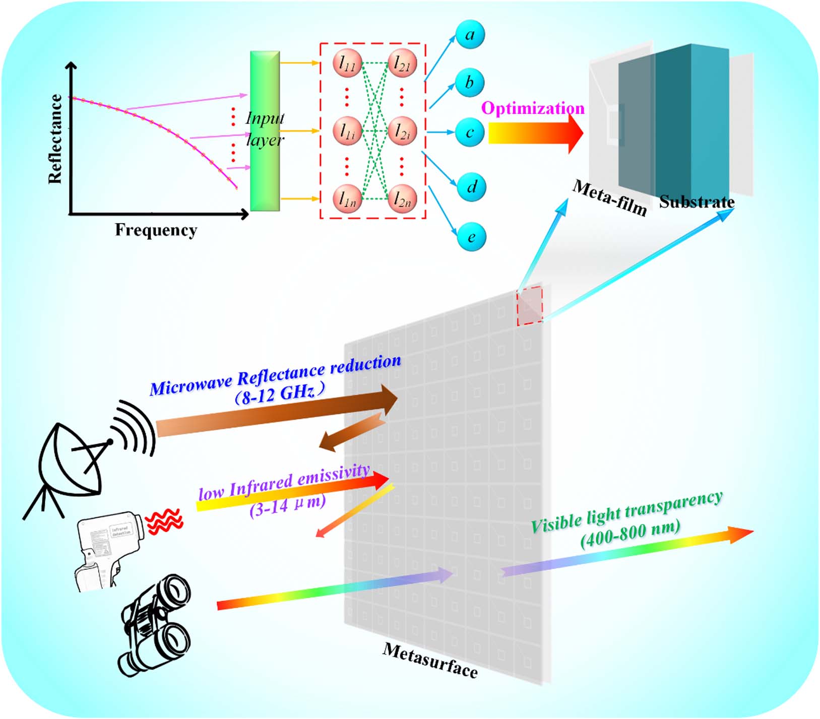
Figure 1.Schematic of this work: a multispectral compatible metasurface is designed via machine learning, which is compatible with VIS, infrared, and microwave frequencies.
2. DESIGN METHODS
A. Structure and NN Design
Figure 2 shows the structure design and BPNN design. Figure 2(a) shows the parameters and materials of the metasurface we designed, which has three layers including the top functional metafilm, the intermediate layer of the dielectric substrate, and the bottom reflected backplane. The indigo dielectric substrate represents the carrier of the metafilm, whose EM parameters are determined according to the specified materials. The magenta regions are the ITO with 10 Ω/sq, and the green regions are polyethylene terephthalate (PET) with a dielectric constant of 3.0 (1–j0.06). Here, we employed the commercial ITO film in which the ITO is attached to PET. The ITO with 10 Ω/sq is put on PET to form a metafilm. The thicknesses of PET t are and of ITO is 185 nm. The other parameters are to be designed, means period size, is the outer boundary of the patch, is the inner boundary of the patch, is the thickness of the dielectric substrate, and is the width of the gap of the patch. Figure 2(b) shows the architectural design of the BPNN, including four layers of neurons, which are the input layer, two hidden layers, and one output layer. The reflectivity curve extracts 1001 values at equal intervals as input; therefore, the input layer contains 1001 neurons. Each of the two hidden layers contains 10 neurons, and the output layer contains 5 neurons. Figures 2(c) and 2(d) show the configuration details of the neuron in the hidden layers where the activated function is a hyperbolic tangent function, and the expression is shown in Eq. (1). Figure 2(e) exhibits the configuration of a neuron in the output layer in which the activated function is a linear transfer function, which is expressed as Eq. (2).
![]()
Figure 2.Structure design: (a) three-dimensional structure diagram and geometrical parameter of the unit, (b) the architecture of BPNN, and (c)–(e) details of neurons.
B. NN Training
![]()
Figure 3.Process and results of NN training: (a) the variation of MSE in the training process, (b) examination of the training process, (c) error histogram of trained network, and (d) the regression plot of all the samples.
C. Structure-Aided Design and Optimization
Herein, an MCM is designed with PMMA as the carrier. Different reflectivity curves are generated and input into the network to test the prediction accuracy of the model. Three nonlinear curves and three nearly linear curves are used as input reflectivity curves, respectively. Six curves are named lines 1–6 in sequence, which are shown in Fig. 4(a). With lines 1–6 input into the NN, the derived parameters are shown in Fig. 4(b), and the 3D views of six corresponding structures are captured in Fig. 4(d). Then, the reflectivity curves of the six structures are simulated, and the simulation results are shown in Fig. 4(d). Figures 4(a) and 4(c) illustrate that the simulation results are consistent with the input curves. Although there is a slight deviation between the prediction and the simulation results, the prediction accuracy of the NN model is still verified. Furthermore, in order to explore the expandability in different scenarios, we employ different dielectric substrate materials [FR4, F4B, and polyimide (PI)] and input reflectivity curves. The materials are F4B ( and ), FR4 ( and ), and PI ( and ). Different datasets for different materials are collected to train the BPNN. In addition, then CST Microwave Studio is used to verify the predicted patterns, and all the processes and results are recorded in Figs. 4(e) and 4(f). The results show that the model still has good accuracy and robustness under different materials, which fully verifies that the architecture we designed has good adaptability for different materials.
![]()
Figure 4.Prediction and verification of structures and EM response by the NN: (a) six generated curves, (b) structural parameters of network prediction, (c) simulation results of the predicted structures, (d) the structures corresponding to the predicted parameters, (e) structural parameters verified by CST program for different materials, and (f) comparison between the input curves and the predicted curves with different materials.
Considering the machining accuracy and the parameters of the commercial dielectric substrate, the structure corresponding to line 1 is further optimized for manufacturing. The resonance of the patch with a gap is mainly located at a gap and an internal junction [50]; therefore, some conductive patches can still be added in the inner blank area to increase the conductive area. Based on structure 1, a further optimization design is carried out, and the final structural parameters are shown in Fig. 5(a) in which the thickness of PET , period size , outer boundary of the patch , inner boundary of the patch , the thickness of the dielectric substrate , and the width of the gap . Compared with the structure in Fig. 2, the ITO area ratio of the optimized structure is increased from 77.08% to 80.51% without affecting the reflectivity. The reflectivity of the structure at different incident angles is obtained by simulation, and the results are shown in Fig. 5(b). In Fig. 5, represents the reflectivity, and represents the absorptivity. and represent the co-polarized reflectivity and cross-polarized reflectivity, respectively. It can be seen from Fig. 5(b) that the reflectivity reduction is achieved at 0°–50° incident angles. In order to explore the causes of reflectivity reduction, the distribution of the electric field and the surface current is monitored, which is shown in Figs. 5(e) and 5(f), respectively. Figure 5(e) shows the distribution of the electric field in the top surface, which illustrates that the ITO surface realizes the enhancement of the electric field and loses the energy of EM waves. Figure 5(f) shows the distribution of the surface current, which illustrates that the surface current has a component in the orthogonal polarization direction. From the above analysis, the reduction of the co-polarization reflectivity is caused by two parts, including EM absorption and orthogonal polarization rotation. Because of multimechanism reflection, the proportion of different components is calculated by reflectivity curves, and the efficiency ratio is recorded in Fig. 5(c). Figure 5(d) is the proportion of energy of each component at 8, 10, and 12 GHz in which the EM absorption and orthogonal polarization conversion reduce the reflectivity of the co-polarization.
![]()
Figure 5.Structure optimization and mechanism analysis: (a) three-dimensional structure diagram and geometrical parameter of the optimized structure, (b) the simulation of co-polarization reflectivity (
After optimizing the geometrical parameters of the sample, the area of the surface conductive layer reaches 80.51%. According to an empirical formula, the emissivity of the samples is related to the proportion of different materials, which can be calculated from Eq. (5) [25,29],
3. EXPERIMENT AND VERIFICATION
In order to further validate the performance of our design, the metafilm is fabricated by a laser carving technique. The commercial ITO is employed as the base material. The ITO with 10 Ω/sq is etched on PET, and the thickness of ITO is 185 nm. The pattern of our design is engraved on the ITO film, and the processing is shown in Fig. 6(a). The commercial ITO film is plated on the whole surface of PET. Therefore, the designed structure regions are reserved, and the regions without structure are etched by laser engraving technology to achieve the prefabricated structure. The fabricated metafilm is presented in Fig. 6(b) from which we can see that the metafilm is transparent. The VIS light transmittance is measured by UV-VIS spectrophotometer Agilent Cary 5000; the measured transmittances of the ITO film and the metafilm at 400–800 nm are recorded in Fig. 6(c). The mean transmittances of the entire ITO and metafilm reach 66% and 68%, respectively, which implies the samples have high transmittance. It is worth mentioning that the fabricated metafilm as shown in Fig. 6(d) is flexible, which can be bent and attached to the curved surface carrier for working.
![]()
Figure 6.Sample fabrication and performance characterization: (a) the processing of the metafilm, (b) the details of the fabricated metafilm, (c) the measurement of VIS light transmittance, and (d) demonstration of the flexible metafilm.
The fabricated metafilm is attached on PMMA, and the microwave measurement is carried out using an anechoic chamber. The measurement environment is presented in Fig. 7(a) in which the sample is placed on the test board and a pair of -band horn antennas are used as receiving and transmitting equipment to measure the reflectivity. The measurement results are captured by a vector network analyzer (Agilent E8363B), which are recorded in Fig. 7(b). A slight misalignment here between the simulation and the measurement may be caused by machining error and edge scattering. Nevertheless, the measurement results still demonstrate that the sample can reduce reflectivity in the X band. Subsequently, as shown in Fig. 7(c), the mean infrared emissivity of the metafilm measured by the TSS-5X infrared emissivity meter is 0.31. To further verify the detailed infrared emissivity in the infrared range of 3–14 μm, an infrared spectrometer is employed to measure the infrared emissivity. The measurement result with equipment is shown in Fig. 7(d), which indicates that the emissivity of the metafilm is 0.3 approximately in the infrared range of 3–14 μm.
![]()
Figure 7.Measurement environment and results: (a) microwave measurement environment, (b) the measured and simulated reflectivities of the sample, (c) the measurement of mean infrared emissivity, and (d) the measurement of infrared emissivity at 3–14 μm.
Furthermore, the thermal radiation performance of the samples at different temperatures is measured by infrared thermal imager G120EX, and the measurement environment is shown in Fig. 8(a) where the four samples are placed on the heating plate. The thermal radiations at 28°C, 50°C, and 100°C are measured, respectively, and the captured results are presented in Figs. 8(b)–8(d). The measurement results show that PET and PMMA have higher thermal radiations, whereas ITO and the metafilm have lower thermal radiations, which fully demonstrates that the designed metafilm has lower infrared thermal radiation performance.
![]()
Figure 8.Measurement of infrared radiation performance: (a) ITO (10 Ω/sq), PMMA, PET, and the metafilm on heating platform, and (b)–(d) infrared radiation detection at 28°C, 50°C, and 100°C.
4. CONCLUSION
Here, we applied a multilayer BPNN to design a metafilm, which can achieve the VIS-infrared-microwave compatibility. The datasets of the metafilm with different dielectric substrates were collected to train the BP network, which makes the network adaptable to different materials. Through training, the mapping between the reflectivity and the structural parameters was successfully established. As an example, PMMA was chosen as the substrate to carry the metafilm. Given a reflectivity curve, the acquisition of its corresponding structural parameters no longer completely depended on the numerical calculation method of simulation software but was directly derived by the inverse design of the NN. In this way, an initial optimization unit was obtained, and the structure was optimized on the basis of considering the processing factors. Finally, the optimized metafilm and PMMA formed the MCM, which can achieve VIS-infrared-microwave compatibility. For VIS light, the mean transmittance of the designed metafilm reached 68% at 400–800 nm. For the infrared, the emissivity of the metafilm is reduced to 0.31; meanwhile, it had low infrared heat radiation. For microwave, the MCM can achieve the reflectivity reduction with the efficiency more than 90% in the X band. The design utility of the BPNN is comprehensively demonstrated via the mapping between reflectivity and structure, also validated by measurement of a multifunctional metasurface involving VIS-infrared-microwave compatibility. Importantly, this architecture can establish the mapping from EM response to electrical structure and was expected to accelerate the design process. In the future, this method can also be extended to the design of phase or polarization, and the metafilm has an important application value in the field of camouflage and protection fields.
APPENDIX A: PREPROCESSES OF THE DATASET
The same reflectivity curves can be generated by different structural parameters, and the structural parameters corresponding to these curves are quite different, that is, the collected source data have nonsingle mapping of parameters and reflectivity curves. As shown in Eq. (
![]()
Figure 9.Euclidean distance matrices: (a) and (c) distance matrices of reflectivity curves, and (b) and (d) distance matrices of structural parameters.
APPENDIX B: TRAINING PROCESSES OF OTHER MATERIALS
In order to demonstrate that the BPNN is effective in more scenarios, we employed the other dielectric substrate materials as carriers to validate the adaptability of the BPNN. The materials are F4B ( and tan ), FR4 ( and ), and PI ( and ). Different datasets for different materials are collected to train the BPNN. Figures
![]()
Figure 10.Performance of BPNN for different materials: (a)–(c) the training states of BPNN for F4B, FR4, and PI materials and (d)–(f) the error of trained BPNN for F4B, FR4, and PI.
References
[1] C. L. Holloway, E. F. Kuester, J. A. Gordon, J. O’Hara, J. Booth, D. R. Smith. An overview of the theory and applications of metasurfaces: the two-dimensional equivalents of metamaterials. IEEE Antennas Propag. Mag., 54, 10-35(2012).
[2] X. Luo. Principles of electromagnetic waves in metasurfaces. Sci. China Phys. Mech. Astron., 58, 594201(2015).
[3] N. Yu, P. Genevet, M. A. Kats, F. Aieta, J.-P. Tetienne, F. Capasso, Z. Gaburro. Light propagation with phase discontinuities: generalized laws of reflection and refraction. Science, 334, 333-337(2011).
[4] L. Huang, X. Chen, H. Mühlenbernd, G. Li, B. Bai, Q. Tan, G. Jin, T. Zentgraf, S. Zhang. Dispersionless phase discontinuities for controlling light propagation. Nano Lett., 12, 5750-5755(2012).
[5] K. Zhang, Y. Wang, S. N. Burokur, Q. Wu. Generating dual-polarized vortex beam by detour phase: from phase gradient metasurfaces to metagratings. IEEE Trans. Microw. Theory Tech., 70, 200-209(2021).
[6] N. I. Landy, S. Sajuyigbe, J. J. Mock, D. R. Smith, W. J. Padilla. Perfect metamaterial absorber. Phys. Rev. Lett., 100, 207402(2008).
[7] J. Hao, Y. Yuan, L. Ran, T. Jiang, J. A. Kong, C. T. Chan, L. Zhou. Manipulating electromagnetic wave polarizations by anisotropic metamaterials. Phys. Rev. Lett., 99, 63908(2007).
[8] D. Schurig, J. J. Mock, B. J. Justice, S. A. Cummer, J. B. Pendry, A. F. Starr, D. R. Smith. Metamaterial electromagnetic cloak at microwave frequencies. Science, 314, 977-980(2006).
[9] X. Li, S. Xiao, B. Cai, Q. He, T. J. Cui, L. Zhou. Flat metasurfaces to focus electromagnetic waves in reflection geometry. Opt. Lett., 37, 4940-4942(2012).
[10] G. A. Rao, S. P. Mahulikar. Integrated review of stealth technology and its role in airpower. Aeronaut. J., 106, 629-642(2002).
[11] H. Ahmad, A. Tariq, A. Shehzad, M. S. Faheem, M. Shafiq, I. A. Rashid, A. Afzal, A. Munir, M. T. Riaz, H. T. Haider, A. Afzal, M. B. Qadir, Z. Khaliq. Stealth technology: methods and composite materials—a review. Polym. Compos., 40, 4457-4472(2019).
[12] F. Ding, Y. Cui, X. Ge, Y. Jin, S. He. Ultra-broadband microwave metamaterial absorber. Appl. Phys. Lett., 100, 103506(2012).
[13] T. J. Cui, M. Q. Qi, X. Wan, J. Zhao, Q. Cheng. Coding metamaterials, digital metamaterials and programmable metamaterials. Light Sci. Appl., 3, e218(2014).
[14] W. Chen, C. A. Balanis, C. R. Birtcher. Dual wide-band checkerboard surfaces for radar cross section reduction. IEEE Trans. Antennas Propag., 64, 4133-4138(2016).
[15] H. L. Zhu, S. W. Cheung, K. L. Chung, T. I. Yuk. Linear-to-circular polarization conversion using metasurface. IEEE Trans. Antennas Propag., 61, 4615-4623(2013).
[16] L. Phan, W. G. Walkup, D. D. Ordinario, E. Karshalev, J.-M. Jocson, A. M. Burke, A. A. Gorodetsky. Reconfigurable infrared camouflage coatings from a cephalopod protein. Adv. Mater., 25, 5621-5625(2013).
[17] L. Yuan, X. Weng, L. Deng. Influence of binder viscosity on the control of infrared emissivity in low emissivity coating. Infrared Phys. Technol., 56, 25-29(2013).
[18] F. Xue, S. Xu, Y.-T. Luo, W. Jia. Design of digital camouflage by recursive overlapping of pattern templates. Neurocomputing, 172, 262-270(2016).
[19] Y. Pang, Y. Shen, Y. Li, J. Wang, Z. Xu, S. Qu. Water-based metamaterial absorbers for optical transparency and broadband microwave absorption. J. Appl. Phys., 123, 155106(2018).
[20] L. Li, R. Xi, H. Liu, Z. Lv. Broadband polarization-independent and low-profile optically transparent metamaterial absorber. Appl. Phys. Express, 11, 52001(2018).
[21] Z. Zhang, M. Xu, X. Ruan, J. Yan, J. Yun, W. Zhao, Y. Wang. Enhanced radar and infrared compatible stealth properties in hierarchical SnO2@ZnO nanostructures. Ceram. Int., 43, 3443-3447(2017).
[22] L. Chen, C. Lu, Y. Zhao, Y. Ni, J. Song, Z. Xu. Infrared emissivities and microwave absorption properties of perovskite Sm0.5Sr0.5Co1−
[23] J. K. Zhang, D. P. Zhao, Z. S. Chen, Y. Liu, H. Wang, Z. Q. Lin, J. M. Shi. One dimensional photonic crystal based multilayer film with low IR and visible signatures. Opt. Mater., 91, 261-267(2019).
[24] D. Qi, X. Wang, Y. Cheng, R. Gong, B. Li. Design and characterization of one-dimensional photonic crystals based on ZnS/Ge for infrared-visible compatible stealth applications. Opt. Mater., 62, 52-56(2016).
[25] H. Tian, H.-T. Liu, H.-F. Cheng. A thin radar-infrared stealth-compatible structure: design, fabrication, and characterization. Chin. Phys. B, 23, 25201(2014).
[26] T. Kim, J.-Y. Bae, N. Lee, H. H. Cho. Hierarchical metamaterials for multispectral camouflage of infrared and microwaves. Adv. Funct. Mater., 29, 1807319(2019).
[27] C. Zhang, J. Yang, W. Yuan, J. Zhao, J. Y. Dai, T. C. Guo, J. Liang, G. Y. Xu, Q. Cheng, T. J. Cui. An ultralight and thin metasurface for radar-infrared bi-stealth applications. J. Phys. D, 50, 444002(2017).
[28] C. Zhang, X. Wu, C. Huang, J. Peng, C. Ji, J. Yang, Y. Huang, Y. Guo, X. Luo. Flexible and transparent microwave–infrared bistealth structure. Adv. Mater. Technol., 4, 1900063(2019).
[29] S. Zhong, L. Wu, T. Liu, J. Huang, W. Jiang, Y. Ma. Transparent transmission-selective radar-infrared bi-stealth structure. Opt. Express, 26, 16466-16476(2018).
[30] Z. Meng, C. Tian, C. Xu, J. Wang, S. Huang, X. Li, B. Yang, Q. Fan, S. Qu. Multi-spectral functional metasurface simultaneously with visible transparency, low infrared emissivity and wideband microwave absorption. Infrared Phys. Technol., 110, 103469(2020).
[31] M. Safari, N. P. Kherani, G. V. Eleftheriades. Multi-functional metasurface: visibly and RF transparent, NIR control and low thermal emissivity(2021).
[32] A. Krizhevsky, I. Sutskever, G. E. Hinton. ImageNet classification with deep convolutional neural networks. Commun. ACM, 60, 84-90(2017).
[33] T. Young, D. Hazarika, S. Poria, E. Cambria. Recent trends in deep learning based natural language processing. IEEE Comput. Intell. Mag., 13, 55-75(2018).
[34] K. He, X. Zhang, S. Ren, J. Sun. Deep residual learning for image recognition. Proceedings of the IEEE Conference on Computer Vision and Pattern Recognition (CVPR), 770-778(2016).
[35] B. Sanchez-Lengeling, A. Aspuru-Guzik. Inverse molecular design using machine learning: generative models for matter engineering. Science, 361, 360-365(2018).
[36] C. C. Nadell, B. Huang, J. M. Malof, W. J. Padilla. Deep learning for accelerated all-dielectric metasurface design. Opt. Express, 27, 27523-27535(2019).
[37] S. An, C. Fowler, B. Zheng, M. Y. Shalaginov, H. Tang, H. Li, L. Zhou, J. Ding, A. M. Agarwal, C. Rivero-Baleine, K. A. Richardson, T. Gu, J. Hu, H. Zhang. A deep learning approach for objective-driven all-dielectric metasurface design. ACS Photon., 6, 3196-3207(2019).
[38] S. An, B. Zheng, H. Tang, M. Y. Shalaginov, L. Zhou, H. Li, M. Kang, K. A. Richardson, T. Gu, J. Hu, C. Fowler, H. Zhang. Multifunctional metasurface design with a generative adversarial network. Adv. Opt. Mater., 9, 2001433(2021).
[39] S. An, B. Zheng, M. Y. Shalaginov, H. Tang, H. Li, L. Zhou, J. Ding, A. M. Agarwal, C. Rivero-Baleine, M. Kang, K. A. Richardson, T. Gu, J. Hu, C. Fowler, H. Zhang. Deep learning modeling approach for metasurfaces with high degrees of freedom. Opt. Express, 28, 31932-31942(2020).
[40] J. Qie, E. Khoram, D. Liu, M. Zhou, L. Gao. Real-time deep learning design tool for far-field radiation profile. Photon. Res., 9, B104-B108(2021).
[41] T. Shan, X. Pan, M. Li, S. Xu, F. Yang. “Coding programmable metasurfaces based on deep learning techniques. IEEE J. Emerg. Sel. Top. Circuits Syst., 10, 114-125(2020).
[42] H. P. Wang, Y. B. Li, H. Li, S. Y. Dong, C. Liu, S. Jin, T. J. Cui. Deep learning designs of anisotropic metasurfaces in ultrawideband based on generative adversarial networks. Adv. Intell. Syst., 2, 2000068(2020).
[43] J. Peurifoy, Y. Shen, L. Jing, Y. Yang, F. Cano-Renteria, B. G. DeLacy, J. D. Joannopoulos, M. Tegmark, M. Soljačić. Nanophotonic particle simulation and inverse design using artificial neural networks. Sci. Adv., 4, eaar4206(2018).
[44] J. Jiang, J. A. Fan. Simulator-based training of generative neural networks for the inverse design of metasurfaces. Nanophotonics, 9, 1059-1069(2020).
[45] W. Ma, F. Cheng, Y. Xu, Q. Wen, Y. Liu. Probabilistic representation and inverse design of metamaterials based on a deep generative model with semi-supervised learning strategy. Adv. Mater., 31, 1901111(2019).
[46] Z. Liu, D. Zhu, S. P. Rodrigues, K.-T. Lee, W. Cai. Generative model for the inverse design of metasurfaces. Nano Lett., 18, 6570-6576(2018).
[47] L. Jiang, X. Li, Q. Wu, L. Wang, L. Gao. Neural network enabled metasurface design for phase manipulation. Opt. Express, 29, 2521-2528(2021).
[48] D. Liu, Y. Tan, E. Khoram, Z. Yu. Training deep neural networks for the inverse design of nanophotonic structures. ACS Photon., 5, 1365-1369(2018).
[49] M. T. Hagan, M. B. Menhaj. Training feedforward networks with the Marquardt algorithm. IEEE Trans. Neural Netw., 5, 989-993(1994).
[50] M. Feng, J. Wang, H. Ma, W. Mo, H. Ye, S. Qu. Broadband polarization rotator based on multi-order plasmon resonances and high impedance surfaces. J. Appl. Phys., 114, 74508(2013).

Set citation alerts for the article
Please enter your email address
© Copyright 2018-2021 | Chinese Laser Press. All Rights Reserved 沪ICP备15018463号-20