
Le Jiang, Xi Luo, Zhongming Luo, Dingjian Zhou, Baoxing Liu, Jincheng Huang, Jianfeng Zhang, Xulin Zhang, Ping Xu, Guijun Li. Interface and bulk controlled perovskite nanocrystal growth for high brightness light-emitting diodes [Invited][J]. Chinese Optics Letters, 2021, 19(3): 030001
- Chinese Optics Letters
- Vol. 19, Issue 3, 030001 (2021)
Abstract
1. Introduction
Halide perovskite luminescent materials have attracted great attention due to their high color purity (narrow emission spectrum), tunable emission color, and solution processibility[
For PeLED fabrication, the solution process is widely used. During the solution process, different solubility of organic solvents that dissolve the perovskite components and ion binding diversity in the solution make it difficult to control the directional crystallization of perovskite crystals[
In this article, we propose an interface and bulk method to control the crystallization process. In terms of interface engineering, ethanolamine (ETA) is doped into the poly(3,4-ethylenedioxy-thiophene):poly-(styrenesulfonate) (PEDOT:PSS) HTL. The intermolecular interaction between the perovskite precursor and the amino-functionalized group of ETA promotes the cubic-shaped crystal growth and passivates halide vacancies through the coordination bonding between the and amino () groups. In terms of bulk morphology engineering, macromolecular polyethylene glycol (PEG) is added to the perovskite precursor to locally confine the nanocrystals and fill pores for high-quality perovskite composite films. As a result, a high brightness of and a high EQE of 13.4% have been achieved for the pure green PeLED simultaneously.
Sign up for Chinese Optics Letters TOC. Get the latest issue of Chinese Optics Letters delivered right to you!Sign up now
2. Results and Discussion
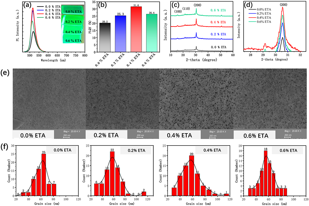
First, we investigate the impact of the surface chemistries and conditions of HTL on the crystal growth of perovskite. Here, HTL is PEDOT:PSS with a different ETA doping concentration. The volume ratio of ETA to PEDOT:PSS is set to be 0%, 0.2%, 0.4%, and 0.6%. Without adding ETA, 0% represents the perovskite EML prepared on PEDOT:PSS. The photoluminescence (PL) spectra of the perovskite EMLs prepared on different volume ratios of ETA/PEDOT:PSS are shown in Fig. 1(a). We can see that the PL intensity increases with the volume ratio of ETA/PEDOT:PSS, reaching the highest value at 0.4%. Continuously increasing the ETA volume concentration will decrease the PL intensity. Furthermore, the addition of ETA in PEDOT:PSS affects the luminescent peak position. With the ETA addition, the emission exhibits a blue shift from 518 nm (without ETA) to 515 nm (0.6%) [inset of Fig. 1(a)]. The PL quantum yield (PLQY) measurement is shown in Fig. 1(b), and it can be seen that the PLQY is only 20.2% without ETA addition, which increases to 31.6% at 0.4% ETA doping. The result of the PLQY is consistent with the PL intensity measurement, revealing that the enhancement of the luminescent property is attributed to the increase of the radiative efficiency (). In principle, the radiative efficiency is given by the following:
![]()
Figure 1.Structural and optical characteristics of CsPbBr3 perovskite films formed on the modified PEDOT:PSS with various ETA ratios. (a) Relative PL spectra and photos of different perovskite films under 400 nm illumination. (b) PLQY of PL. (c) XRD patterns. (d) XRD patterns of crystal orientation (200). (e) SEM images. (f) Grain size.
Here, is the radiative recombination time constant, and is the non-radiative recombination time constant. It is clear that the enhancement of the radiative efficiency can be due to either the enhancement of the radiative recombination or the suppression of the non-radiative recombination.
To shed light on the mechanism that dominates the improvement of the radiative efficiency, the effect of ETA modified PEDOT:PSS on the perovskite film’s crystal structure is measured by X-ray diffraction (XRD). A series of XRD spectra of the perovskite films is shown in Fig. 1(c). It can be seen that the XRD pattern of the perovskite films formed on the ETA-doped PEDOT:PSS is similar to that of the perovskite film formed on PEDOT:PSS without adding ETA, showing three typical characteristic peaks at 14.95°, 21.38°, and 30.30°, which correspond to the (100), (110), and (200) crystal planes of the cubic . The XRD pattern suggests a preferred crystallization along the (200) crystal plane, and its intensity increases with the increasing ETA concentration. However, when the ETA volume concentration is increased to 0.6%, the XRD intensity of the (200) plane decreases, as shown in Fig. 1(d). Figure 1(e) shows the scanning electron microscope (SEM) images of perovskites on different HTLs. The SEM images show remarkable changes in the morphology. When PEDOT:PSS is used, the perovskite shows large grains. The crystal grain growth is incomplete, and the grain distributes densely. With ETA addition, perovskite growth is complete, showing cubic-shaped nanocrystals with distinguished grain edges. However, when the volume ratio is increased to 0.6%, some of the grains collapse and convert from cubic to rectangular morphology. The change of the perovskite morphology is attributed to the improved surface wetting property and the molecular interaction between the ETA and perovskite precursor. Previous reports have suggested that the interaction can induce the deprotonation of the excess cations surrounding the corner sharing octahedron, giving rise to more uniform cubic-shaped nanocrystals[
These results show that interface engineering with ETA can enhance perovskite crystallization and promote the passivation of defects. The enhanced radiative recombination can be attributed not only to the increased crystallinity, but also to the amino-functionalized group of ETA. ETA molecules have the amino () groups, which have the potential to passivate the surface halide vacancies through the coordination bonding between exposed and amino () groups[
The PeLED is prepared with PEDOT:PSS as the HTL and 2,2′,2′′-(1,3,5-benzinetriyl)-tris(1-phenyl-1-H-benzimidazole) (TPBi)/LiF as the ETL. Figure 2(a) is the schematic device structure of (ITO, 100 nm)/HTL (30 nm)/perovskite (50 nm)/TPBi (50 nm)/LiF (1 nm)/Al (100 nm). Figure 2(b) shows the normalized electroluminescence (EL) spectra for PeLEDs. The emission peak of the ETA-modulated device shows a blue shift from 518 nm (without ETA doping) to 515 nm (0.4% and 0.6%), which is consistent with the variation of the PL spectra. The blue shift of the emission peak suggests the removal of the shallow traps of the perovskite EML. However, the blue shift may also be caused by changes in the perovskite grain size. The narrow emission width of 19 nm proves the high crystallinity of the perovskite nanocrystals. Figures 2(c)–2(f) show the characteristic EL performance of PeLEDs prepared on different HTLs.
![]()
Figure 2.Device performance of PeLEDs fabricated on ITO-glass with various ETA ratios in PEDOT:PSS. (a) Device structure of the PeLED. (b) EL spectrum for the PeLED with CsPbBr3 as the EML. (c) J-V and (d) L-V characteristics. (e) CE as a function of luminance. (f) EQE as a function of luminance.
The detailed luminescence data are shown in Table 1. The current density–voltage (J-V) in Fig. 2(c) and brightness–voltage (L-V) curves in Fig. 2(d) show that, under the same bias voltage, the current density and brightness of the PeLEDs with the ETA modified PEDOT:PSS (0.4% and 0.6%) are both higher than that of the device without using ETA. The increase of the current density injection for the ETA-modulated devices mainly originates from the porous morphology, giving rise to the high leakage current. Even then, high brightness of is still achieved for this porous morphological device, manifesting the enhanced radiative recombination and suppressed non-radiative recombination. The high brightness gives rise to high current efficiency (CE) of 22.35 cd/A and high EQE of 7.21% [Figs. 2(e) and 2(f)], both of which are obtained when the ETA doping ratio is 0.4%, agreeing with the PL and PLQY results.
| ETA Ratio (%) | Luminance (cd/m2)/Voltage (V) | CE (cd/A) | EQE (%)/Voltage (V) |
|---|---|---|---|
| 0.0 | 6897/6.2 | 8.88 | 2.75/4.0 |
| 0.2 | 14,037/6.2 | 11.99 | 4.45/5.0 |
| 0.4 | 27,968/6.2 | 22.35 | 7.21/4.2 |
| 0.6 | 20,198/6.0 | 16.72 | 5.84/4.2 |
Table 1. Summary of the EL Performance of the PeLEDs with Different ETA Doping Concentrations
Although interfacial engineering with ETA-modulated PEDOT:PSS results in the growth of cubic-shaped nanocrystals with high crystallinity, the porous morphology may also lead to current leakage due to the direct contact between HTL and ETL. Therefore, it is necessary to control the bulk perovskite growth towards a more compact morphology. Therefore, we further introduce the macromolecular polymer PEG into the perovskite precursor. The as-obtained PEG-doped perovskite film exhibits high brightness, as can be seen from the inset of Fig. 3(a). The enhanced brightness is characterized by the PL measurement. With PEG doping, the PL intensity increases, reaching a maximum value at a doping concentration of 20 mg/mL. A high doping concentration of 30 mg/mL decreases the PL intensity. The optimal doping concentration of 20 mg/mL corresponds to a maximum PLQY of 54.8%, compared with a value of 39% for perovskite without PEG doping [Fig. 3(b)].
![]()
Figure 3.Structural and optical characteristics of CsPbBr3 perovskite films with various PEG ratios. (a) Relative PL spectra and photos of different perovskite films under 400 nm illumination. (b) PLQY of PL. (c) XRD patterns. (d) XRD patterns of crystal orientation (200). (e) SEM images. (f) Grain size.
To further understand the improvement of PL properties with PEG doping, XRD and SEM are used to illustrate the changes of crystallinity and morphology of perovskite films [Figs. 3(c), 3(d), and 3(e)]. There are three prominent diffraction peaks at 14.95°, 21.38°, and 30.30°, which correspond to the (100), (110), and (200) crystal planes, respectively. With PEG doping, the XRD peak position does not change. However, the crystallinity decreases with the increase of the PEG concentration. The peak intensity increases again when the PEG concentration increases to 30 mg/mL. The decrease of the crystallinity is a result of the reduction of the grain size, as revealed by the SEM images [Fig. 3(e)]. The grain size statistics in Fig. 3(f) demonstrate that the main grain size reduces from 70 nm (0 mg/mL PEG) to 60 nm (10 mg/mL) to 40 nm (20 mg/mL). Large-sized crystal particles appear when the PEG concentration is 30 mg/mL, which is supported by the increased crystallinity from the XRD spectrum. In addition to the decreased XRD intensity, another apparent feature from the SEM result is that the perovskite film becomes dense and compact when decreasing the grain size with PEG. It is well known that PEG is a Lewis base, which can coordinate with the lead ions of perovskite, which is considered to facilitate passivating the point defects and enhancing the luminescence of perovskite. Additionally, the growth of perovskite crystal is confined within a localized space and crosslinks the grain size to obtain a smooth and compact morphology, which helps to reduce the leakage current.
PeLEDs are fabricated to evaluate the effect of the perovskite nanocrystal morphology on the device performance. As shown in Fig. 4(a), all devices exhibit the same emission spectrum centered at 516 nm, along with a narrow emission width of 19 nm. It is a pure green emission with the International Commission on Illumination (CIE) coordinates of (0.107,0.763) [Fig. 4(b)]. Figures 4(c)–4(f) are the characteristic performances including J-V, L-V, CE-J, and EQE-J. From the J-V curves [Fig. 4(c)], we can see that the PEG doping largely decreases the leakage current because of the dense and compact morphology that prevents direct contact between HTL and ETL. For 10 mg/mL and 20 mg/mL PEG doping concentrations, the brightness is enhanced [Fig. 4(d)]. However, the high CE is only obtained at the PEG doping concentration of 20 mg/mL, manifesting that the leakage current is successfully inhibited only with the dopant condition of 20 mg/mL. Table 2 summarizes the device parameter obtained from Figs. 4(c)–4(f). Without PEG, the device exhibits a maximum brightness of , a maximum CE of 34.08 cd/A, and a peak EQE of 9.49%. With PEG doping, the turn-on voltage () is reduced from 2.8 V to 2.6 V. With 20 mg/mL PEG, the device shows a maximum brightness of at 5.4 V, CE of 45.52 cd/A, and 13.44% maximum EQE.
| PEG Concentration (mg/mL) | Luminance (cd/m2)/Voltage (V) | CE (cd/A) | EQE (%)/Voltage (V) |
|---|---|---|---|
| 0.0 | 48,529/4.8 | 34.08 | 9.49/3.8 |
| 10.0 | 55,736/5.6 | 39.04 | 11.24/3.6 |
| 20.0 | 64,756/5.4 | 45.52 | 13.44/3.4 |
| 30.0 | 46,554/5.8 | 27.16 | 8.17/4.0 |
Table 2. EL Performance of the PeLEDs with Different PEG Concentrations in Perovskite-Emitting Layers
![]()
Figure 4.(a) EL spectrum for the PeLED with PEG:CsPbBr3 as the EML. (b) The 1931 International Commission on Illumination (CIE) color coordinate. (c) J-V and (d) L-V characteristics. (e) CE as a function of luminance. (f) EQE as a function of luminance.
In summary, we have demonstrated the interface and bulk control of the morphology of the perovskite nanocrystals toward high brightness and high-efficiency PeLEDs. The ETA-modulated PEDOT:PSS interface approach confirmed the critical role of the interfacial effect on perovskite crystallization and defect passivation. ETA-doped PEDOT:PSS triggered the formation of high-quality perovskite films with high crystallinity and cubic-shaped nanocrystals, resulting in the enhancement of the radiative recombination and the suppression of the non-radiative losses. The bulk approach using macromolecular polymer PEG as the dopant of the perovskite precursor successfully improved perovskite EML with a smooth and compact morphology and reduced the leakage current by preventing the direct contact between ELT and HTL. These results provide a new defect passivation method for improving perovskite LEDs’ performance and have a particular significance for the development of other perovskite-based electronic devices.
3. Experimental Section
PLQY = Photon emitted/Photon absorbed. (The minimum measurement value can be 0.1%.)
The PLQY of the perovskite films was measured using Enlitech LQ-100X equipment with a 450 W xenon lamp as the excitation source. The following settings were applied for PLQY measurements: excitation wavelength of 400 nm, laser delay of 20 ms, and source delay of 2000 ms, respectively, with step increments of 1 nm. We measured the light intensity with a laser power meter, and the estimated light power density incident on the samples was about .
References
[4] C. T. Wang, K. Chen, P. Xu, F. Yeung, H. S. Kwok, G. Li. Fully chiral light emission from CsPbX3 perovskite nanocrystals enabled by cholesteric superstructure stacks. Adv. Funct. Mater., 29, 1903155(2019).
[12] Y. Lin, L. Shen, J. Dai, Y. Deng, Y. Wu, Y. Bai, X. Zheng, J. Wang, Y. Fang, H. Wei, W. Ma, X. C. Zeng, X. Zhan, J. Huang. π-conjugated Lewis base: efficient trap-passivation and charge-extraction for hybrid perovskite solar cells. Adv. Mater., 29, 1604545(2017).
[19] B. Ren, G. Yuen, S. Deng, L. Jiang, D. Zhou, L. Gu, P. Xu, M. Zhang, Z. Fan, F. Sze, Y. Yueng, R. Chen, H.-S. Kwok, G. Li. Multifunctional optoelectronic device based on an asymmetric active layer structure. Adv. Funct. Mater., 29, 1807894(2019).

Set citation alerts for the article
Please enter your email address
© Copyright 2018-2021 | Chinese Laser Press. All Rights Reserved 沪ICP备15018463号-20