
Sajid Hussain, Ahmad Raza, Fawad Saeed, Abida Perveen, Yan Sikhai, Nasrud Din, Elias E. Elemike, Qianqian Huang, Alagesan Subramanian, Qasim Khan, Wei Lei. Stable and high performance all-inorganic perovskite light-emitting diodes with anti-solvent treatment[J]. Chinese Optics Letters, 2021, 19(3): 030005
- Chinese Optics Letters
- Vol. 19, Issue 3, 030005 (2021)
Abstract
1. Introduction
Organic and inorganic halide perovskites have attracted a lot of attention due to their extensive use in various applications and optoelectronic properties like broad band wavelength absorption, high photoluminance (PL), narrow full width at half-maximum (FWHM), band gap tunability, intrinsic photophysical stability[
For example, cesium lead bromide () polycrystalline film-based Pe-LEDs offer an auspicious substitute technique to increase the device performance due to their higher thermal stability compared with organic-based perovskite methylammonium lead bromide ()-based Pe-LEDs. However, sensitivities to humidity, light, and heat are still the main challenges facing Pe-LEDs[
However, energy level matching and unbalanced charge carrier injection are also serious issues hindering the high efficiency of perovskite-based optoelectronic devices[
Sign up for Chinese Optics Letters TOC. Get the latest issue of Chinese Optics Letters delivered right to you!Sign up now
Through a simple spin-coating technique, we have successfully designed and manufactured inverted perovskite LEDs with higher performance and stability. To improve the surface morphology, PL, and interfacial interaction between the transporting layers and active layer, a simple post-treatment strategy of applying MA while spinning, is followed by another solvent known as the anti-solvent, i.e., CB. As a result, the devices showed a low turn-on voltage () of 2.0 V and maximum luminance of at current efficiency of . This initiative suggests a simple way to adjust rate of the carriers’ injection along with reducing surface defects in optoelectronic devices and lighting technologies based on perovskites for their high resolution displays and cost-effective technology.
2. Experimental Section
The patterned fluorine-doped tin oxide (FTO) substrates were cleaned with detergent, deionized (DI) water, acetone, EtOH, and IPA for 15 min each using the ultrasonication cleaner and treated with UV ozone for 30 min before use. The ETL ZnO nanoparticles (NPs) ( in butanol, filtered through a 0.22 µm N66 filter) were spin-coated on the substrate at 2000 r/min for 40 s and annealed at 140°C for 10 min. The active layer perovskite precursor solution CsBr and with a molar ratio of 1.2:1 (0.3 mol/L) was mixed in anhydrous dimethyl sulfoxide (DMSO) (80°C, 4 h, 800 r/min), spun onto the ZnO NPs at 2000 r/min for 50 s along with the dropped MA delay of 5 s after starting the spin coater, and finally treated with an anti-solvent CB perovskite layer with same speed. Afterward, poly-TPD ( in chloroform) as an HTL was spin-coated onto the perovskite film at 2500 r/min for 40 s. Finally, Au was deposited by thermal deposition through a shadow mask. The active area of our fabricated devices was . All of the fabrication was done in ambient conditions.
3. Result and Discussion
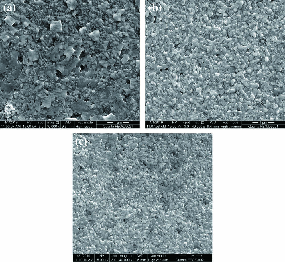
Fabrication of the uniform, continuous, and pinhole-free film remains a challenge. Scanning-electron microscopy (SEM) images of perovskite film in Fig. 1(a) reveal that the as prepared film is discontinuous on ZnO NPs. The coverage of the polycrystalline is too poor because of the high crystallization rate of the perovskites. By observation through SEM images, it is roughly estimated that the entire coverage of perovskite film without any solvent treatment was very low, which is reliable with a previously reported treatment onto ZnO NPs[
![]()
Figure 1.Scanning electron microscopy (SEM) images of perovskite films (a) without MA, (b) with dropped MA after delay of 5 s, and (c) treated with anti-solvent CB and MA.
In order to investigate the crystal structure, an X-ray diffraction (XRD) measurement of perovskite film deposited on the FTO was performed. The XRD patterns of film prepared with and without solvent treatment are shown in Fig. 2(a). All of the samples show similar perovskite properties, and all crystallographic features are in good agreement with the orthorhombic tetragonal phase.
However, good crystallographic properties are exhibited when dropping anti-solvent CB onto the MA-treated perovskite film, which is also evidence of improved device performance. High performance of Pe-LEDs can be understood by the effective improvement in the fluorescence quantum efficiency, which can be improved by solvent treatment of the perovskite film. A good comparison between the PL emission of films with/without solvent behavior is shown in Fig. 2(b). An instant transition has been noted at around 524.5 nm in the PL emission band with narrow FWHM of 17 nm for all of the perovskite films, with a difference of enhanced PL emission with solvent-treated films, whereas, PLQYs with anti-solvent-treated perovskite film are , which is higher than those without solvent-treated films of . Figure 2(c) shows PL images under the UV light at 365 nm, which signifies that with solvent treatment we can obtain a film with small and closely packed grains, which enhances the surface coverage and quality of perovskite film, ultimately enhancing the performance of the device.
![]()
Figure 2.(a) X-ray diffraction (XRD) patterns without MA/CsPbBr3, with MA/CsPbBr3, and with MA/CsPbBr3 treated with anti-solvent CB. (b) Normalized PL, (c) PL image only with MA-treated perovskite film, and (d) PL image of perovskite film treated with CB and MA.
The inverted Pe-LEDs with either pristine or post-treated (EML) were fabricated, as shown in Figs. 3(a) and 3(b) with the following structure: FTO//Poly-TPD/Au. An anti-solvent CB was dropped onto the MA-treated perovskite film in order to increase the morphology and surface coverage; this device is denoted as “#4”. For comparison, we tested with same structure without dropping the anti-solvent CB onto the solvent-treated MA perovskite film and the device is denoted as “#3”; whereas, we understand the mechanism of the perovskite film as a reference device with only solvent-treated CB, denoted as “#2”. Any device without any solvent treatment is denoted as “#1”. Here FTO, ZnO, poly-TPD, and Au are used as the cathode, ETLs, HTLs, and anode, respectively.
![]()
Figure 3.(a) Energy level diagram of the Pe-LEDs. (b) Schematic of device structure.
The performance of -based devices is visualized and summarized in Fig. 4 and Table 1. Figures 4(a)–4(d) represent the summarized characteristics of the devices with and without anti-solvent treatment. Figure 4(a) shows the current density–voltage (J-V) characteristics of all of the fabricated devices. The lowest current density (J) of device #4 is an indication of the crystalline perovskite film blocking the short-circuit current paths in the device, as revealed in the SEM images. The better surface coverage of the perovskite film in turn results in higher device performance due to better charge injection in the EML. The compared luminance performances of the Pe-LEDs are shown in Fig. 4(b). The improvement in luminance of device #4 with anti-solvent-treated perovskite film, as compared to that of devices #1, 2, and 3, indicates that the minimized short circuit as well as an incredible enhancement in CE is found, as shown in Fig. 4(c), and the higher external quantum efficiency (EQE) for device #4 [Fig. 4(d)] is dedicated to the improved surface morphology and affects the performance of the device due to solvent treatment.
| Device No. | Structure | CEmax (cd·A−1) | EQEmax (%) | ||
|---|---|---|---|---|---|
| 1 | FTO/ZnO/CsPbBr3 (with/without MA)/poly-TPD/Au | 2.4 | 11,088 | 35.6 | 5.7 |
| 2 | FTO/ZnO/CsPbBr3 (with CB)/poly-TPD/Au | 2.4 | 12,622 | 36.1 | 5.9 |
| 3 | FTO/ZnO/CsPbBr3 (with MA)/poly-TPD/Au | 2.1 | 16,855 | 40.4 | 7.1 |
| 4 | FTO/ZnO/CsPbBr3 (with MA)-dropped CB/poly-TPD/Au | 2.0 | 17,866 | 45.8 | 8.3 |
Table 1. Characteristics of the Measured Pe-LED Devices
![]()
Figure 4.Comparison results: (a) J-V, (b) luminance-V, (c) CE-V, and (d) EQE-V.
The stability of all of the devices was measured in ambient conditions at 50% humidity without any encapsulation. Figure 5(a) describes the details of the stability results, where device #4 shows excellent stability when compared to the rest of the devices. The surplus of electrons due to greater mobility of ZnO as compared to the low hole mobility of poly-TPD induces high electron conductivity, resulting in increased exciton quenching and reduced radioactive recombination in the active region. Besides, the charge unbalance into the EML is also one of the major causes to make the LED device unstable and with low efficiency. To check the carrier’s injection mechanism into the EML, we studied the hole-only device (HOD) and electron-only device (EOD), showing the well-balanced charge injection and the improved device performance, as shown in Fig. 5(b).
![]()
Figure 5.(a) Stability characteristics of different devices and (b) comparison between the HODs and EODs.
4. Conclusion
We have presented a simple and facile method for obtaining high quality perovskite film for efficient Pe-LEDs. Dropping anti-solvent CB onto MA treated film can gain high coverage of the active layer with nanocrystal growth in ambient conditions. The fast crystallization rate has a diverse effect on device performance and its stability. Pe-LEDs treated with solvent exhibit luminance of and current efficiency of , which is one of the highest efficiencies of all Pe-LEDs solution-based inorganic , and also show strong stability. Most significantly, the film treated with solvent is efficient and more durable against environmental moisture and oxygen, which is a promising material for the fabrication of all-inorganic -based LEDs with high efficiency.
References
[1] K. Qasim, B. Wang, Y. Zhang, P. Li, Y. Wang, S. Li, S. T. Lee, L. S. Liao, W. Lei, Q. Bao. Solution-processed extremely efficient multicolor perovskite light-emitting diodes utilizing doped electron transport layer. Adv. Funct. Mater., 27, 1606874(2017).
[6] C. Wu, Y. Zou, T. Wu, M. Ban, V. Pecunia, Y. Han, Q. Liu, T. Song, S. Duhm, B. Sun. Improved performance and stability of all-inorganic perovskite light-emitting diodes by antisolvent vapor treatment. Adv. Funct. Mater., 27, 1700338(2017).
[7] P. Xia, Y. Lu, Y. Li, W. Zhang, W. Shen, J. Qian, Y. Wu, W. Zhu, H. Yu, L. Liu, L. Deng, S. Chen. Solution-processed quasi-two-dimensional/nanoscrystals perovskite composite film enhances the efficiency and stability of perovskite light-emitting diodes. ACS Appl. Mater. Interfaces, 12, 39720(2020).
[17] L. Tang, J. Qiu, Q. Wei, H. Gu, B. Du, H. Du, W. Hui, Y. Xia, Y. Chen, W. Huang. Enhanced performance of perovskite light-emitting diodes via diamine interface modification. ACS Appl. Mater. Interfaces, 32, 29132(2019).
[18] Q. Huang, J. Pan, Y. Zhang, J. Chen, Z. Tao, C. He, K. Zhou, Y. Tu, W. Lei. High-performance quantum dot light-emitting diodes with hybrid hole transport layer via doping engineering. Opt. Express, 24, 25955(2016).
[20] S. Hussain, A. Subramanian, S. Yan, G. Abbas, A. Shuja, W. Lei, Q. Khan. Engineering architecture of quantum dot-based light emitting diode for high device performance with double-sided emission fabricated by non-vacuum technique. ACS Appl. Electron. Mater., 8, 2383(2020).
[21] W. J. E. Beek, M. M. Wienk, M. Kemerink, X. Yang, R. A. J. Janssen. Hybrid zinc oxide conjugated polymer bulk heterojunction solar cells. J. Phys. Chem. B, 19, 9505(2005).

Set citation alerts for the article
Please enter your email address
© Copyright 2018-2021 | Chinese Laser Press. All Rights Reserved 沪ICP备15018463号-20