
Min ZHONG, Xian-Chun SHI. Realization of a multiband metamaterial waveguide based on dirac semimetal in the 800~1100nm range [J]. Journal of Infrared and Millimeter Waves, 2020, 39(5): 576
- Journal of Infrared and Millimeter Waves
- Vol. 39, Issue 5, 576 (2020)
Abstract
Introduction
Electromagnetic metamaterials reveal many unique properties, which can’t be achieved in nature materials, such as, cloaking, negative refraction index, or lensing [
In this paper, a tunable MDM waveguide based on Dirac semimetal layers is designed and simulated in the 800~1100nm range. This waveguide reveals four transmission peaks. These transmission peaks are excited by the interference effect between the main cavity and cavities 1, 2, 3, or 4. Since the dielectric constant of Dirac semimetal is sensitive to Fermi energy, resonance wavelenths of transmission peaks can be modulated by changing the Fermi energy. Therefore, the tenability of this waveguide is verified in the 800~1100nm range.
1 Design and model
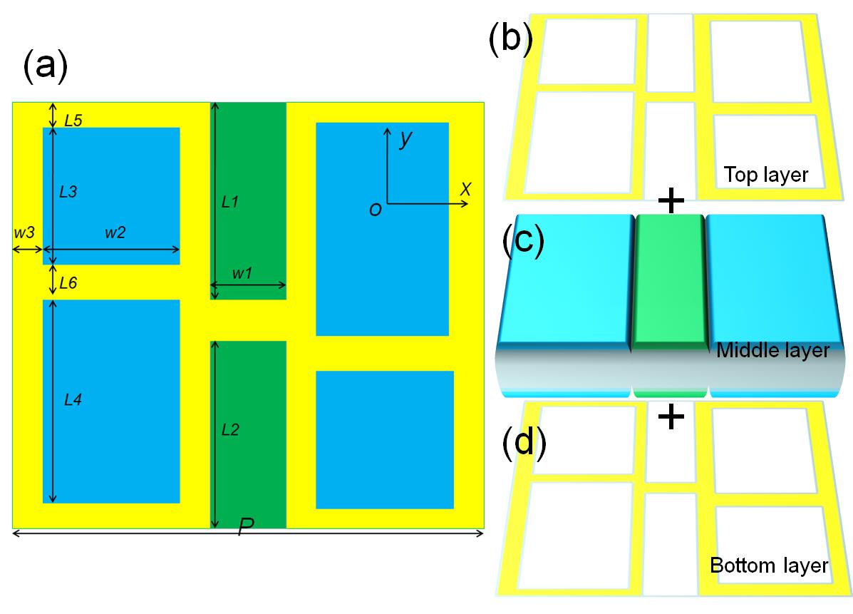
The proposed metal–insulator–metal waveguide is shown in Fig 1. A reflecting layer is added in the main cavity of the waveguide, which plays as a waveguide modulator. Detailed structural parameters are given in table 1. In this unit cell, two Dirac semimetal layers are described as follows [
where, is set to be Fermi level, is set to be Fermi momentum, Fermi velocity stands for . Moreover, the permittivity of two Dirac semimetal layers is given as follows [
Based on the reported work [
In the equation above, propagation constant of SPP modes is set to be . Ideal boundaries are set based on the reported work [29].
![]()
Figure 1.(a) Schematic diagram of the proposed metal–insulator–metal waveguide. The yellow parts are Dirac semimetal layers. The green part is SU-8 layer. The blue part is SiO2. (b) The top layer of the proposed unit cell. (c) The middle layer of the proposed unit cell. (d) The bottom layer of the proposed unit cell. The thickness of SU-8 layer and SiO2 layer is set as 180nm
| P | w1 | L1 | L2 | L3 | L4 | w2 | w3 | |
|---|---|---|---|---|---|---|---|---|
| 300 | 30 | 140 | 140 | 110 | 150 | 80 | 12 |
Table 1. 几何参数
2 Results and discussion
The simulated transmission spectrum of the proposed metamaterials waveguide is shown in Fig 2(b), see the black line. Four transmission peaks are achieved at resonance wavelengths 842nm, 921nm, 1010nm, and 1061nm, respectively. The amplitudes of these transmission peaks are: 70%, 61%, 72%, and 63%, respectively. This waveguide reveals multi-band transmission behaviors. For ease of description, these transmission peaks are labeled as: P1, P2, P3, and P4, respectively. It is found that the P1 and P3 are higher than the P2 and P4. These transmission peaks are all narrow bands.
![]()
Figure 2.(a) The schematic diagram of the proposed structure. (b) Simulated and calculated transmission spectrum of the proposed structure. (c) Schematic diagram of the waveguide without metal reflector layer. (d) Simulated and calculated transmission spectrum of the waveguide without metal reflector layer
In order to reveal the physical mechanism of these transmission peaks, magnetic field intensity distributions are calculated separately at the resonance wavelengths. For the P1 peak, magnetic field intensity distribution is calculated at resonance wavelength 842nm, as shown in Fig 3(a). It is found that the simulated magnetic field is mainly distributed in the main cavity and the Cavity 1. In contrast, there is substantially no magnetic field distributed in the cavities 2, 3, and 4. Moreover, the magnetic field distributed in the main cavity is coupled with that in the Cavity 1, which results in the P1, as shown in Fig 2(a). In order to better explain the effect of the coupling between different cavities on transmission peaks, the phase spectrum of the proposed metamaterials waveguide is also calculated, as shown in Fig 5. Four phase values close to zero are achieved at resonance wavelengths 842nm, 921nm, 1010nm, and 1061nm. For the P1 peak, the phase value is 0.04. When the electromagnetic wave in the main cavity is coupled with that in the Cavity 1, the phase value is close to zero, which results in the enhancement of the transmission, as shown in Fig 3(a). In contrast, when the calculated wavelength is deviated from the resonance wavelength, the transmission of the electromagnetic wave is reduced obviously, as shown in Fig 2(b). At the same time, the magnetic field intensity is mainly distributed in the main cavity due to the strong interference conditions are destroyed, as shown in Fig 3(c). In order to better understand the relationship between the coupling resonance behavior and the transmission peak, the transmission spectrum of this waveguide is calculated based on the coupled mode theory. The transmission amplitudes of the main cavity and the Cavities 1, 2, 3, and 4 are set to be A, B, C, D, and E. Thesetransmission amplitudes can be defined as follows [
where, , , , , and are set to be the resonant frequencies of the main cavity, and cavities (1, 2, 3 and 4), is set to be the loss factor. Therefore, the transmission of the proposed metamaterials waveguide is given as follows:
According to the equation above, when the calculated frequency is satisfied as follows:
Then, interference conditions between the main cavity and the Cavity 1 are achieved, which leads to the transmission enhance and the P1. Therefore, when the calculated frequency deviates from the resonance frequency of Cavity 1 , the transmittance is suppressed, as shown in Fig 2(b) and Fig 3(a).
![]()
Figure 3.(a) The magnetic field intensity distribution at resonance wavelength 842nm. (b) The magnetic field intensity distribution at resonance wavelength 921nm. (c) The magnetic field intensity distribution at resonance wavelength 900nm. (d) The magnetic field intensity distribution at resonance wavelength 950nm
At the resonance position of the P2, magnetic field intensity is mainly distributed in the main cavity and the Cavity 2, as shown in Fig 3(b). The magnetic field intensity in the cavities 1, 3, and 4 is weekly. Moreover, the phase difference is also close to zero at the resonance position of the P2, as shown in Fig 5. It is revealed that the transmission is enhanced by interference between the main cavity and the Cavity 2, which results in the P2. When the calculated frequency is deviated from the resonance frequency of Cavity 2 , the interference conditions between the main cavity and the Cavity 2 are failure, the transmission is reduced and the electromagnetic wave energy is blocked by the reflective layer, as shown in Fig 3(d). For the transmission peaks P3 and P4, transmission interference strength phenomenons between the main cavity and the Cavities 3 or 4 are also can be found when the conditions or are achieved, as shown in Fig 4(a-b). Moreover, the phase differences are also close to zero at the resonance position of the P3 or P4, as shown in Fig 5.
![]()
Figure 4.(a) The magnetic field intensity distribution at resonance wavelength 1010nm. (b) The magnetic field intensity distribution at resonance wavelength 1061nm. (c) The magnetic field intensity distribution at resonance wavelength 1040nm. (d) The magnetic field intensity distribution at resonance wavelength 1080nm
![]()
Figure 5.The phase spectrum of the proposed structure
The proposed waveguide contains a Dirac semimetal reflector (A short metal bar located in the middle of Dirac semimetal layers), as shown in Fig 2(a). It is obvious that the electromagnetic wave energy is blocked by the Dirac semimetal reflector and can’t penetrate the waveguide cavity, as shown in Fig 3(c~d) and Fig 4(c~d). Therefore, this reflector in the proposed metamaterials waveguide plays a transmission band selector. To reveal the effect of this Dirac semimetal reflector, a waveguide without this reflector is also designed and simulated, as shown in Fig 2(c~d). It is found that two transmission valleys are revealed at resonance wavelengths 885nm and 973nm, respectively, as shown in Fig 2(d). The magnetic field intensity of the waveguide without reflector is achieved in Fig 6. It is found that most of electromagnetic wave energy is travelled along the waveguide cavity in transmission bands, as shown in Fig6 (a~b). However, electromagnetic wave energy is blocked at the front metal layer the waveguide without reflector, as shown in Fig 6(c-d).
![]()
Figure 6.(a) The magnetic field intensity distribution of the waveguide without metal reflector layer at resonance wavelength 840nm. (b) The magnetic field intensity distribution of the waveguide without metal reflector layer at resonance wavelength 940nm. (c) The magnetic field intensity distribution of the waveguide without metal reflector layer at resonance wavelength 885nm. (d) The magnetic field intensity distribution of the waveguide without metal reflector layer at resonance wavelength 973nm
On the one hand, according to Equation (4), it can be known that the dispersion equation of SPP modes is related to the permittivity of the proposed waveguide. On the other hand, the proposed waveguide is made of Dirac semimetal, and the permittivity of this material is sensitive to Fermi energy. Therefore, the resonance properties of the waveguide can be modulated by changing the Fermi energy. To verify the tunability of this waveguide, different Fermi energies are used. The simulated transmission spectrum is shown in Fig 7. The Fermi energy of Dirac semimetal layers is enhanced from 50meV to 70meV. It is found that all of transmission peaks are enhanced. Moreover, these transmission peaks are shifted to lower resonance wavelengths, which confirms the tunable of this proposed waveguide. The real and imaginary parts of the permittivity of Dirac semimetals layers are shown in Fig 8. It is revealed that the real part of the permittivity is reduced with the Fermi energy of Dirac semimetal layers increasing, as shown in Fig 8. The perturbation theory can be used to reveal the relationship between the resonance wavelengths and the permittivity of Dirac semimetals layers [
Based on the simulated results in Fig 8, as the Fermi energy increasing, the real part of the dielectric constant is reduced, which results in the is lower than zero. According to the equation (14), the resonance frequency is enhanced (resonance wavelength is shifted to shorter wavelengths) due to the is lower than zero, as shown in Fig 7. It should be noted that these transmission peaks cannot achieve perfect transmission, as shown in Figures 2 and 7, mainly due to the high imaginary part of the permittivity of Dirac semimetals, which leads to the inevitable energy loss of electromagnetic waves. However, the permittivity of the Dirac semimetal is sensitive to Fermi energy, as shown in Fig 7. Therefore, this material can be used to design and develop a tunable metamaterial waveguide. At the same time, simulation results also show that the transmittance of this tunable metamaterial waveguide can be enhanced by adjusting Fermi energy, as shown in Figure 7.
![]()
Figure 7.Transmission spectrum with different Fermi energy
![]()
Figure 8.(a) Imaginary parts of the permittivity of Dirac semimetals layers. (b) Real parts of the permittivity of Dirac semimetals layers
3 Conclusion
In conclusion, a tunable metamaterial waveguide is numerically investigated with Dirac semimetal layers. Four transmission peaks (70%, 61%, 72%, and 63%) are achieved in the 800~1100nm range. Simulated results reveal that these transmission peaks are originated from the interference effect between the main cavity and the Cavities 1, 2,3, or 4. Four transmission peaks can be tuned through changing the Fermi energy. The proposed metamaterial waveguide may have application in nanoscale filter, switch, or refractive index sensor.
References
[1] C Liu, P Liu, C Yang et al. Analogue of dual-controlled electromagnetically induced transparency based on graphene metamaterial. Carbon, 142, 354-362(2019).
[2] D R Smith, J B Pendry, M C K Wiltshire, Metamaterials and. Science, 305, 788-792(2004).
[3] X He, Y Yao, X Yang et al. Dynamically controlled electromagnetically induced transparency in terahertz graphene metamaterial for modulation and slow light applications. Opt. Commun, 410, 206-210(2018).
[4] M Badioli, A Woessner, K J Tielrooij et al. Phonon-mediated mid-Infrared photoresponse of grapheme. Nano Lett, 14, 6374-6381(2014).
[5] T Liang, Q Gibson, M Ali et al. Ultrahigh mobility and giant magnetoresistance in the Dirac semimetal Cd3As2. Nat. Mater, 14, 280-284(2015).
[6] S M Zhong, S L He, Ultrathin and, SCIENTIFIC REPORTS. Ultrathin and lightweight microwave absorbers made of mu-near-zero metamaterials, 3, 2083-2087(2013).
[7] Z D Yong, S L Zhang, C S Gong et al. Narrow band perfect absorber for maximum localized magnetic and electric field enhancement and sensing applications. Scientific Reports, 6, 24063-24069(2016).
[8] J Mei, G C Ma, M Yang et al. Dark acoustic metamaterials as super absorbers for low-frequency sound. Nature communications, 3, 756-762(2011).
[9] Y P Zhang, T T Li, Q Chen et al. Independently tunable dualband perfect absorber based on graphene at mid-infrared frequencies. Scientific Reports, 5, 18463-18470(2015).
[10] G T Cao, H J Li, S P Zhan et al. Uniformtheoretical description of plasmon-induced transparency in plasmonic stubwaveguide. Opt. Lett, 39, 216-219(2014).
[11] Y Deng, G T Cao, Y W Wu et al. Theoretical description of dynamic transmission characteristics in MDM waveguide aperture-side-coupled with ring cavity. Plasmonics, 10, 1537-1543(2015).
[12] G Lai, R S Liang, Y J Zhang et al. Doubleplasmonic nanodisks design for electromagnetically induced transparencyand slow light. Opt. Express, 23, 6554-6561(2015).
[13] Z He, H Li, B Li et al. Theoretical analysis of ultrahighfigure of merit sensing in plasmonic waveguides with a multimode stub. Opt.Lett, 41, 5206-5209(2016).
[14] Y Huang, C J Min, G Veronis. Broadband near total light absorption innon-PT-symmetric waveguide-cavity systems. Opt. Express, 24, 22219-22231(2016).
[15] L Chen, Y M Liu, Z Y Yu et al. Numerical analysis of anear-infrared plasmonic refractive index sensor with high figure of meritbased on a fillet cavity. Opt. Express, 24, 9975-9983(2016).
[16] A B Yankovich, R Verre, E Olsén et al. Electron-Energy Loss Study of Nonlocal Effects in Connected Plasmonic Nanoprisms. ACS Nano, 11, 4265-4274(2017).
[17] C Zeng, Y D Cui. Rainbow trapping of surface plasmon polariton waves in metal-insulator-metal graded grating waveguide. Opt Commun, 290, 188-191(2013).
[18] L L Huang, X Z Chen, B F Bai et al. Dependent Directional Surface Plasmon Polariton Excitation Using A Metasurface with Interfacial Phase Discontinuity. Light-Sci. Appl, 2, 70-76(2013).
[19] H X Fu, S L Li, Y Wang, Let al. Generation of polarization-locked vector solitons in mode-locked thulium fiber laser. IEEE Photonics J, 10, 1500308-1500316(2018).
[20] S L Li, Y L Wang, R Z Jiao et al. Fano resonances based on multimode and degenerate mode interference in plasmonic. Opt. Exp, 25, 3525-3533(2017).
[21] Z Chen, L Yu, Multiple Fano. IEEE Photonics J, 6, 1-8(2014).
[22] C Li, S L Li, Y L Wang et al. Multiple Fano Resonances Based on Plasmonic Resonator System With End-Coupled Cavities for High-Performance Nanosensor. IEEE Photonics J, 9, 1-9(2017).
[23] Q Wang, Z B Ouyang, M Lin et al. Independently tunable Fano resonance based on the coupled hetero cavities in a plasmonic MIM system. Materials, 11, 1675-1684(2018).
[24] G Zheng, H Zhang, L Bu et al. Tunable Fano resonances in midinfrared waveguide-coupled otto configuration. Plasmonics, 13, 215-220(2018).
[25] X C Yia, J P Tiana, R C Yanga, Tunable Fano. Optik - International Journal for Light and Electron Optics, 171, 139-148(2018).
[26] O V Kotov, Y E Lozovik, Dielectric response. Phys. Rev. B, 93, 235417(2016).
[27] T Timusk, J P Carbotte, C C Homes et al. Three-dimensional Dirac fermions in quasicrystals as seen via optical conductivity. Phys. Rev. B, 87, 235121(2013).
[28] I Zand, A Mahigir, T Pakizeh et al. Selective-mode optical nanofilters based on plasmonic complementary split-ring resonators. Opt. Express, 20, 7516-7525(2012).
[29] D R Smith, S Schult, P Markos et al. Determination of effective permittivity and permeability of metamaterials from reflection and transmission coefficients. Phys.Rev. B, 65, 195104-195108(2002).
[30] X J Piao, S Yu, S Koo et al. Fano-type spectral asymmetry and its control for plasmonic metal-insulator-metal stub structures. Opt. Express, 19, 10907-10912(2001).
[31] Y Yao, M A Kats, P Genevet et al. Broad electrical tuning of grapheneloaded plasmonic antennas. Nano Lett, 13, 1257-1264(2013).
[32] Z Li, N Yu, Modulation of. Appl. Phys. Lett, 102, 131108(2013).
[33] J Hwang, J W Roh, Electrically tunable. Opt.Express, 25, 25071-25078(2017).

Set citation alerts for the article
Please enter your email address
© Copyright 2018-2021 | Chinese Laser Press. All Rights Reserved 沪ICP备15018463号-20