Significance Continuous miniaturization of traditional silicon electronic devices and photoelectric components increases the integration and performance of devices and introduces some undesirable problems caused by the size and quantum effects, and increased power consumption. Thus, the development of multifunctional next-generation nano-devices with more excellent performance than traditional devices is inevitable and significant in the post-Moore era. Owing to the excellent mechanical, thermal, electrical, and optical properties of nanomaterials, such as nanoparticles, quantum dots, nanowires, nanotubes, and two-dimensional (2D) materials, many studies have suggested that these materials are suitable for channel or electrode of multifunctional and high-performance nano-devices. Thus, the study and development of nano-devices based on nanomaterials are crucial for solving the bottleneck problems of electronics in the future.
Recently, abundant theoretical and experimental results have demonstrated that bending, folding, twisting a single nanomaterial, and arranging, assembling, connecting several nanomaterials can improve properties further or bring extraordinary characteristics of nano-devices. For instance, compared with chemical doping and contact engineering, deformation of 2D materials can solve the Fermi-level pinning and carrier concentration decreasing in nano-devices and may introduce new phenomena, such as piezotronics and piezo-phototronics. Thus, methods and accompanying systems for moving, arranging, deforming nanomaterials, and fabricating nano-structures and nano-devices will be crucial and indispensable in the electronics field in the future. The most “top-down” approaches for fabricating electronic and optoelectronic devices, such as ultraviolet lithography, electron beam lithography, and laser writing, are unfit for the mentioned purpose. Instead, nano-manipulation technology, as a “bottom-up” method, is proposed to move or spin atoms, nanomaterials, and cells in the nanoscale resolution. Based on this, it is promising in moving, deforming, and assembling nanomaterials in high-precision than other methods. For example, some indirect methods for bending 2D materials (e.g., thermal expansion mismatch, deformation of flexible substrates, and substrate surface topography modification) exist some problems, such as slipping of materials, small deformation, and uncontrollability. Nano-manipulation can use probes to push or fold materials in nano-/micro-scale directly and achieve large, complex, and controllable deformation. With electron beam-induced deposition, laser processing, and nano-welding, this technology can also develop nano-structures with excellent properties, weld a single material onto an electrode to fabricate devices, and test properties of a single material and device. Thus, it provides a new idea for the development of new-generation nano-devices with excellent performance.
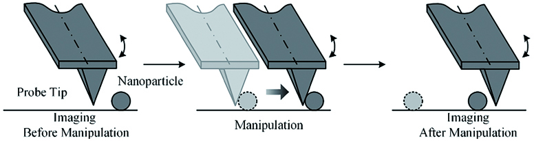
Among many nano-manipulation techniques, methods and systems based on the microscopes with nano-level imaging accuracy, e.g., scanning probe microscope (SPM) and electron microscope (EM), are widely used. With the microscope monitor, the system controls the motion module to move the probes, tweezers and other manipulation tools in high-precision, and then moves, picks up, and bends nanoparticles (NPs), nanowires (NWs), and 2D materials. Besides, optical tweezers, magnetic tweezers, and acoustic tweezers can apply force to materials and trap or move these further by controlling the optical, magnetic, and sound fields. To develop nano-devices, manipulation methods based on SPM, EM, and optical tweezers are promising and anticipated. Thus, it is necessary and significant to introduce and summarize the recent studies in these nano-manipulation methods and understand their application in nano-devices.
Progress This study introduces the recent research in nano-manipulation based on scanning probe microscope(SPM), electron microscope(EM), and optical tweezers. For SPM manipulation, the principles and typical process demonstrate the capacity for accurately moving particles of tens to a few nanometers in diameter and weakness in real-time imaging, efficient and complex manipulation. For real-time imaging during manipulation, representative improvements include strategy optimization and development of parallel imaging/manipulation system (
Conclusions and Prospects SPM manipulation, EM manipulation, and optical tweezers have their advantages, limitations, and applications (