
Xun Li, Ming Li, Hongjun Liu. Enhanced optical absorption surface of titanium fabricated by a femtosecond laser assisted with airflow pressure[J]. Chinese Optics Letters, 2021, 19(9): 091404
- Chinese Optics Letters
- Vol. 19, Issue 9, 091404 (2021)
Abstract
Keywords
1. Introduction
Due to their high strength, low specific gravity, corrosion resistance, and other advantages, titanium (Ti) and its alloys are the most important materials for aerospace, marine, automotive, biomedical, and so on. Recently, metal surfaces with micro/nanostructures have found many potential applications in the fields of antireflection[
Many techniques have been proposed to produce reproducible antireflective metal surfaces with micro/nanostructures[
In this paper, an effective and easy method was proposed to achieve enhanced optical absorption surface of Ti alloy 7 (Ti7) fabricated by a fs laser assisted with airflow pressure. The effect of laser scanning speed and laser power on the surfaces’ morphology and average reflectivity was studied. By introducing different airflow pressure in the fs laser manufacturing process of Ti7, an ultralow average reflectance of 2.31% over the 250–2300 nm spectral range was obtained. In addition, the average reflectivity of samples fabricated under different laser parameters assisted with airflow was shown, and the influence of airflow pressure on the formation and evolution of light-absorbing micro/nanostructures was discussed. Finally, the high and low temperature tests (HLTTs) of all samples were performed to test the stability performance of the hybrid micro/nanostructures in extreme environments.
Sign up for Chinese Optics Letters TOC. Get the latest issue of Chinese Optics Letters delivered right to you!Sign up now
2. Experimental Setup
2.1. Materials
A Ti7 sample with a size of was used in our experiments. The mechanically polished surface of the sample was cleaned in an ultrasonic cleaner with anhydrous ethanol and deionized water before laser treatment.
2.2. Preparation of the micro/nano hybrid structures
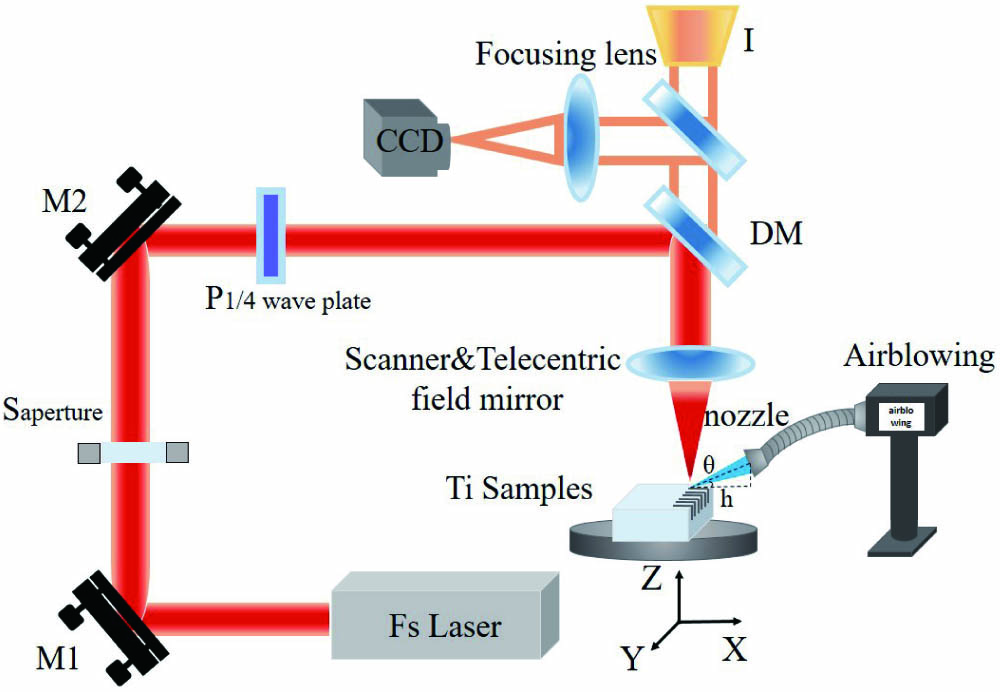
Figure 1 presents the experimental setup of the fs laser fabrication assisted with airflow pressure. After the laser passed through the (0–12 mm aperture adjustable) and the , it was split into two beams by the , where 95% of the laser beam entered the two-dimensional scanning galvanometer and focused on the working surface for sample processing, and 5% of the laser beam was focused to the CCD through the measuring industrial lens for processing observation and precise focusing. The airblowing device was placed next to the sample, the distance from the nozzle to the surface was 10 mm, and the angle of incidence was 30°.
![]()
Figure 1.Schematic of the fs laser processing system assisted with airflow pressure.
For metal surface modification, an industrial fs laser (Pharos-20 W from Light Conversion, Lithuania) with a high repetition rate of 1 MHz and the highest power of 20 W was employed. The laser pulse width was 290 fs at a wavelength of 1030 nm. An galvanometric scanner (SCANCUBE14, Scanlab, Germany) was used to control the laser beam and focused by a telecentric field mirror (, TL-1064-20-65, Lenstek Laser Optics, China). The diameter of the focused spot defined by the intensity dropped to of the maximum value that was approximately 20 µm. An air compressor was used to control airflow pressure (PO-0.75LES5C, Hitachi, Japan).
2.3. Measurement and characterization
The three-dimensional morphology of the micro/nanostructures induced by the fs laser on the surface of the metal was characterized by a tungsten filament electron microscope (JSM-IT500LA, JEOL, Japan), field emission scanning electron microscopy (JSM-7900 F/SU8010, JEOL/Hitachi, Japan), and confocal microscopy (VK-X1000,Keyence, Japan), respectively. The reflectance of laser-treated Ti samples in the UV, visible, and NIR regions (250–2300 nm) was measured by using a spectrophotometer (UV-3600, Shimadzu Corporation, Japan). The chemical composition of the sample was characterized by X-ray diffraction (XRD) (D8 advance A25, Bruker, Germany). In addition, the stability of hybrid micro/nanostructures was tested in a high–low temperature chamber (SET-Z-022U, Shanghai Espec Environmental Equipment, China), the parameters of which were low temperature at and high temperature at 50°C, where each temperature lasted 3 h, and the high and low temperature cycle lasted 72 h.
3. Results and Discussion
Firstly, the impact of the scanning velocity on the morphology of micro/nanostructures was studied, as displayed in Fig. 2. The laser power was fixed at 20 W, while the laser scanning velocity was increased from 20 mm/s to 60 mm/s. As the scanning speed was lower at 20 mm/s, the overlap rate of laser pulse was high, and the massive accumulation of energy raised the temperature within the laser-irradiated region, which resulted in the melting of Ti7 and ablation plume from the substrate. Therefore, the continuous V-groove structures were formed, which were deemed to be one of the light-absorbing structures, as shown in Fig. 2(a). When the scanning speed increased to 30 mm/s, the total fluence of pulses per spot () declined, which caused the weakening of the laser material interaction and then led to the change of surface morphology from continuous microgrooves to a discontinuous slot. It leads to the microgrooves occupying the whole surface to only part of it, as illustrated in Fig. 2(b). When laser ablation weakened as the scanning velocity increased to 40 mm/s, the discontinuous stripe distribution on the surface was further reduced, and micropores became the main form, as presented in Fig. 2(c). Then, as the further decreased under 50 mm/s scanning velocity, the discrete distributed hybrid structures were formed, which consisted of many kinds of protrusions/cavities and deep holes, the max depth of which was 73.95 µm, as shown in Fig. 3(e). For the case of the highest scanning speed, attributed to the fluence decreasing to a relatively low range, as shown in Fig. 2(d), the depth of the microstructure was reduced to 58.58 µm. In addition, it is also observed that the melting effect on the nanostructures was reduced with the acceleration of scanning speed[
![]()
Figure 2.Three-dimensional morphology of the samples fabricated by the fs laser at different scanning speeds: (a) 20 mm/s, (b) 30 mm/s, (c) 40 mm/s, and (d) 60 mm/s.
![]()
Figure 3.Laser power dependence of three-dimensional micro/nanostructures’ morphology: (a) 2.5 W, (b) 5 W, (c) 10 W, (d) 15 W, and (e) 20 W.
Then, the effect of the fs laser pulse energy on the micro/nanostructures’ morphology of Ti7 samples was investigated. In our experiments, the scanning velocity and repetition rate were fixed at 50 mm/s and 50 kHz, while the average power varied from 2.5 W to 20 W. Figure 3 shows the morphology of the samples fabricated by the fs laser at different power. It is found that the whole micro/nanostructures were stray distribution in all cases. With the increase of pulse energy, the process of laser ablation was intensified, and the bulges and microholes gradually emerged, the depth of which could be up to 73.95 µm in the case of 20 W, as distributed in Fig. 3(e). Moreover, it is also observed that the nanostructure period induced by the fs laser became smaller as the laser power increased, which was mainly due to the enhancement of energy absorption between surface plasmon polaritons (SPPs) and incident light[
Figure 4 exhibits the reflection spectra of the samples fabricated by the fs laser at different laser power and scanning speed. For all of the cases at different laser processing parameters, the trend of reflectance over the wavelength range was basically the same. However, there were also some differences for each case, which was mainly attributed to the formation of different micro/nanostructures at different processing conditions, as displayed in Figs. 2 and 3. In all the cases, the lowest average reflectivity over the wavelength range from 250 nm to 2300 nm was 2.83% for the case of 20 W and 50 mm/s. When the average power was reduced to 2.5 W, the average reflectivity gradually increased to 4.96%, the maximum reflectance of which was 7.59% in the NIR 2047 nm wavelength. The main reason is that with the higher laser power, the deeper microstructures were generated on the surface of the samples, as presented in Fig. 2. According to the Fresnel scattering theory[
![]()
Figure 4.Reflection spectra of the samples with hybrid micro/nanostructures induced by the fs laser at different laser power and scanning speed.
As for fixing the laser power but changing the scanning speed, the decrease in sample reflectivity was also different. When the scanning velocity was increased to 50 mm/s, the lowest average reflectivity was 2.83%, while it was 3.12% for the case of 20 mm/s. It is implied that the regular microgrooves provided fewer multi-reflection processes and had a weaker ability to capture light scattering. In addition, the average reflectivity for the cases of 30 mm/s and 40 mm/s was higher than that of the 20 mm/s case. The basic groove pattern with some micropores was distributed on the surface for the cases of 30 mm/s and 40 mm/s. However, the depth of the micropore was not deep enough to form an effective optical cavity. For the highest scanning speed of 60 mm/s in our experiments, the reflection of the sample reached up to 3.87%. The reason for this phenomenon lies in the number and depth of microstructures that were distinctly reduced as the accumulated energy decreased. Due to the limited number of microstructures, the sample did not have enough cavities to capture light beams in all directions and produced less absorption, which weakened the light trapping effect. Therefore, the number and the depth of microstructures were proved to be two of the most important factors influencing the light trapping effect.
In order to further reduce the reflectivity of metal, the effect of airflow pressure on the reflectivity was investigated. At a fixed scanning velocity of 50 mm/s and 20 W average power, the micro/nanostructures were fabricated on the samples by the fs laser assisted with air pressure. Figure 5 displays the morphology of samples fabricated by the fs laser under different airflow pressures. It is obvious that the depth and quantity of the microstructure and the morphology of the nanostructure had changed under different airflow pressures.
![]()
Figure 5.Three-dimensional micro/nanostructures’ morphology of samples fabricated by the fs laser assisted with different airflow pressures: (a) 0 MPa, (b) 0.05 MPa, (c) 0.1 MPa, and (d) 0.15 MPa.
As the airflow pressure changed to 0.05 MPa, the number of microstructures increased significantly, and the microstructures’ depth increased from 73.951 µm to 82.686 µm. The period of the nanostructure remained unchanged, but its morphology was more abundant, which evolved from nanoprotrusion to nanovilli. With the further increase of the airflow pressure to the 0.1 MPa, the depth of the microstructure increased to the deepest of 92.125 µm, while the nanostripe distribution period became shorter. The phenomenon mentioned above is attributed to the temperature and pressure of the interface during laser–material interactions being changed, which subsequently changed the mechanisms of the microstructures’ formation and plasma plume formation[
For the airflow pressure at 0.15 MPa, the depth of the microstructure decreased to 81.364 µm, and the nanovilli structure disappeared. The main reasons for the influence of airflow pressure on the morphology of micro/nanostructures are as follows. First, an excessively large airflow exerts pressure on the plasma plume, which causes the plasma plume to tilt along the direction of the airflow, changing the depth and morphology of the micro/nanostructure. Figure 5(d) presents obviously that the micro/nanostructure had a 60° airflow scouring morphology. Also, excessive airflow would reduce the redeposition of micro/nanometer particles and inhibit the bubble burst[
![]()
Figure 6.Changing mechanism of the micro/nanostructures' morphology by airflow pressure.
Figure 7 exhibits the reflection spectra of the samples fabricated by the fs laser under different airflow pressures. It is apparent that the reflection of the samples assisted with the airflow pressure treatment was obviously suppressed in the range from 250 nm to 2300 nm. When the air pressure rose from 0 MPa to 0.1 MPa, the average reflectivity of the samples decreased significantly from 2.83% to 2.31%. This is attributed to the increase of the microstructures’ depth from 73.951 µm to 92.125 µm, which greatly strengthened the light trapping effect. Also, the period of the abundant nanostripes became shorter under higher air pressure assistance, which had a positive effect on the further reduction of the reflectance of specific wavelengths. However, when the airflow pressure was further increased to 0.15 MPa, the average reflectance increased from 2.31% to 2.59%. This phenomenon is because the depth of the surface microstructures decreased to 81 µm, which affected the number of reflections of light in the trap structure for Fresnel scattering. Moreover, according to Figs. 5 and 6, the redeposition of nanoparticles was greatly reduced. It is believed that more nanostructures could result in smaller filling factors, which could act as effective medium layers to alleviate the optical impedance mismatch between the solid substrates and air[
![]()
Figure 7.Reflection spectra of the samples fabricated by the fs laser under different airflow pressures.
From the analysis mentioned above, it is demonstrated that the airflow pressure has an important influence on the micro/nanostructures for light trapping. Moreover, it should be noted that the reflectance of the sample fabricated at 0.05 MPa was significantly increased in the wavelength range of 200–400 nm. This is because insufficient pressure prevented the nanostructures from producing richer stripes, but the deposition of nanoparticles was reduced. Therefore, when blackening metals, the appropriate gas pressure should be selected under specific laser processing parameters, because the reflectance of the sample was the balance of many factors such as the morphology and depth of the microstructure, nanostripe, and nanoparticle deposition.
In order to identify the mechanism leading to the enhancement of light absorption on the Ti surface fabricated by the fs laser assisted with air flow pressure, a detailed study on the elemental composition of samples used XRD characterization. By analyzing the chemical composition of samples prepared with different airflow pressures, the evidence for oxide metal elements such as (PDF#04-007-2177), (PDF#04-004-6417), (PDF#04-003-2923), (PDF#04-089-0552), TiO (PDF#04-006-1902), and (PDF#00-003-1122) were found on the surface of micro/nanostructures, which was produced by the reaction, since the Ti7 ablation by the laser is done in air[
![]()
Figure 8.XRD patterns of sample surfaces with different airflow pressures at 20 W and 50 mm/s.
![]()
Figure 9.Blackening samples of Ti alloy before and after HLTTs.
In order to further verify the influence of air pressure on sample reflectivity, the effect of airflow pressure on the surface’s morphology and their reflectivity under different fs laser parameters was investigated. Table 1 shows the average reflectivity of samples fabricated under different laser parameters assisted with airflow before and after the HLTT. It is shown that airflow obviously improves the average reflectivity under different processing parameters. Compared with the cases without airflow, the average reflectivity of the samples obtained under the airflow pressure had a significant reduction, the decrease of which varied from 0.1% to 0.72%. For different laser parameters, the pressure of airflow at which the lowest reflectivity of the sample can be obtained was different. The lowest average reflectivity of samples fabricated by 2.5 W and 5.0 W fs lasers was obtained under 0.05 MPa, while it was obtained at 0.1 MPa between 10 W and 20 W. As for different scanning speeds, the lowest average reflectance of samples made at 60 mm/s was obtained at 0.05 MPa, while the lowest reflectance of samples fabricated at other scanning speeds was obtained under 0.1 MPa. This phenomenon is attributed to the reason that the energy of the laser incident on the sample surface and the overlap rate of the spot were changed under different laser processing parameters that assisted with the same airflow pressure, which led to different laser heat accumulation and the cooling and solidification processes. Also, the redeposition of micro/nanoparticles of plasma generated under different laser parameters was different.
| Parameter | Reflectivity/% | |||||||
|---|---|---|---|---|---|---|---|---|
| 0 MPa | 0.05 MPa | 0.1 MPa | 0.15 MPa | |||||
| Before | After | Before | After | Before | After | Before | After | |
| 2.5 W, 50 mm/s | 4.96 | 5.10 | 4.47 | 4.67 | 4.58 | 4.77 | 4.81 | 5.01 |
| 5.0 W, 50 mm/s | 4.39 | 4.55 | 3.88 | 4.01 | 3.91 | 4.06 | 4.19 | 4.32 |
| 10 W, 50 mm/s | 4.15 | 4.25 | 3.95 | 4.06 | 3.86 | 3.99 | 3.92 | 4.05 |
| 15 W, 50 mm/s | 3.58 | 3.81 | 3.22 | 3.45 | 3.17 | 3.21 | 3.24 | 3.38 |
| 20 W, 50 mm/s | 2.83 | 2.97 | 2.45 | 2.59 | 2.31 | 2.43 | 2.59 | 2.71 |
| 20 W, 20 mm/s | 3.12 | 3.28 | 3.05 | 3.15 | 2.46 | 2.61 | 2.85 | 2.99 |
| 20 W, 30 mm/s | 4.23 | 4.45 | 3.79 | 3.97 | 3.53 | 3.77 | 3.69 | 3.81 |
| 20 W, 40 mm/s | 4.09 | 4.29 | 3.82 | 4.09 | 3.49 | 3.71 | 3.75 | 3.94 |
| 20 W, 60 mm/s | 3.87 | 3.94 | 3.15 | 3.25 | 3.31 | 3.41 | 3.59 | 3.72 |
Table 1. Average Reflectivity of Samples Fabricated Under Different Laser Parameters Assisted with Airflow Before and After High and Low Temperature Tests
For practical applications, blackened metals are used in harsh environments, such as the light-absorbing surface of various optoelectronic systems in aerospace. In order to test the stability performance of the hybrid micro/nanostructures in extreme environments, the HLTTs of all samples were performed. After a dust-proof treatment, twelve high and low temperature cycles (72 h) were conducted from to 50°C (each temperature lasted for 3 h). Under temperature gradient changing, the thermal stress relief of the material substrate was generated, which resulted in a slight change in the morphology and depth of the micro/nanostructures. It is found that the maximum depth of microstructures was still 92 µm, but the number of micro/nanostructures with maximum depth had decreased. Moreover, the surface chemical analysis was conducted after the HLTT test, as depicted in Fig. 9. The strongest peak position of XRD patterns of the sample had not changed before and after HLTT, indicating that its oxide composition had not changed. The sample had already formed an oxide layer on the surface after laser processing, and, since the oxide layer isolated the metal from the air, the performance of the oxide composition was stable. If it is necessary to further increase the oxide type and film thickness on the Ti alloy surface, special high-temperature treatment was required. The maximum temperature used in HLTT was only 50°C, which was much lower than the temperature used for high-temperature oxidation of Ti alloy (the oxide of Ti alloy starts to form at the lowest temperature of 200°C). After the HLTT, the average reflectivity of all samples had a slight increase of about 0.06%–0.27%, which was mainly ascribed to the change in the number of microstructures with the greatest depth caused by the thermal stress relief of the material substrate. As for the minimum average reflectance, the sample increased slightly from 2.31% to 2.43%.
4. Conclusions
In summary, an effective method was proposed to achieve an enhanced optical absorption surface of Ti7 by fs laser fabrication assisted with airflow pressure. Three-dimensional morphology and the average reflectivity of the samples fabricated by the fs laser at different scanning speed and laser power were discussed. The effect of airflow pressure on the samples’ average reflectivity was investigated. In order to test the stability performance of the hybrid micro/nanostructures in extreme environments, HLTTs of all samples were performed. An explanation for the low average reflectivity of the samples obtained by this method was given. It is demonstrated that (1) the morphology of the samples fabricated by the fs laser changed greatly under different airflow pressure; (2) the samples’ reflectivity was obviously reduced in the case of larger single pulse energy or slower scanning speed assisted with airflow pressure; (3) the sample achieved by this method has a stability performance of optical absorption. In the future, more studies will be carried out to investigate the effect of the direction of airflow on the reflection performance of samples fabricated by the fs laser.
References
[1] J. X. Fu, H. Liang, J. Y. Zhang, Y. B. Wang, Y. N. Liu, Z. Y. Zhang, X. C. Lin. Enhanced optical absorbance and fabrication of periodic arrays on nickel surface using nanosecond laser. Opt. Commun., 389, 170(2017).
[2] P. X. Fan, B. F. Bai, M. L. Zhong, H. J. Zhang, J. Y. Long, J. P. Han, W. Q. Wang, G. F. Jin. A general strategy towards dual-scale controlled metallic micro-nano hybrid structures with ultralow reflectance. ACS. Nano., 11, 7401(2017).
[3] B. Zheng, W. Wang, G. Jiang, K. Wang, X. Mei. Fabrication of broadband antireflective black metal surfaces with ultra-light-trapping structures by picosecond laser texturing and chemical fluorination. Appl. Phys. B, 122, 180(2016).
[4] A. Y. Vorobyev, C. Guo. Femtosecond laser blackening of platinum. J. Appl. Phys., 104, 053516(2008).
[5] A. Y. Vorobyev, C. L. Guo. Enhanced absorptance of gold following multipulse femtosecond laser ablation. Phys. Rev. B, 72, 195422(2005).
[6] M. H. Dar, R. Kuladeep, V. Saikiran, D. N. Rao. Femtosecond laser nanostructuring of titanium metal towards fabrication of low-reflective surfaces over broad wavelength range. Appl. Surf. Sci., 371, 479(2016).
[7] I. Etsion. State of the art in laser surface texturing. J. Tribol. Trans., 127, 248(2005).
[8] J. R. Zhang, W. T. Lin, Y. C. Guan, X. N. Gu. Biocompatibility enhancement of Mg-Gd-Ca alloy by laser surface modification. J. Laser Appl., 31, 022510(2019).
[9] J. R. Zhang, G. Q. Hu, L. B. Lu, Y. C. Guan, M. H. Hong. Enhancing protein fluorescence detection through hierarchical biometallic surface structuring. Opt. Lett., 44, 339(2019).
[10] S. Yang, K. Yin, J. Wu, Z. Wu, D. Chu, J. He, J. Duan. Ultrafast nano-structuring of superwetting Ti foam with robust antifouling and stability towards efficient oil-in-water emulsion separation. Nanoscale, 11, 17607(2019).
[11] K. Yin, D. Chu, X. Dong, C. Wang, J. Duan, J. He, S. Yang, K. Yin, J. Wu, Z. Wu, D. Chu, J. He, J. Duan. Femtosecond laser induced robust periodic nanoripple structured mesh for highly efficient oil–water separation. Nanoscale, 9, 14229(2017).
[12] G. Q. Li, J. W. Li, Y. L. Hu, C. C. Zhang, X. H. Li, J. R. Chu, W. H. Huang. Realization of diverse displays for multiple color patterns on metalsurfaces. Appl. Surf. Sci., 316, 451(2014).
[13] H. P. Wang, M. J. He, H. Liu, Y. C. Guan. One-step fabrication of robust superhydrophobic steel surfaces with mechanical durability, thermal stability, and anti-icing function. Appl. Mater., 11, 25586(2019).
[14] K. C. Park, H. J. Choi, C. H. Chang, R. E. Cohen, G. H. Mckinley, G. Barbastathis. Nanotextured silica surfaces with robust superhydrophobicity and omnidirectional broadband supertransmissivity. ACS Nano, 6, 3789(2012).
[15] Y. X. Song, C. Wang, X. R. Dong, K. Yin, F. Zhang, Z. Xie, D. K. Chu, J. A. Duan. Controllable superhydrophobic aluminum surfaces with tunable adhesion fabricated by femtosecond laser. Opt. Laser Technol., 26, 34016(2018).
[16] H. Wu, Y. L. Jiao, C. C. Zhang, C. Chen, L. Yang, J. W. Li, J. C. Ni, Y. C. Zhang, C. Z. Li, Y. Y. Zhang, S. J. Jiang, S. W. Zhu, Y. L. Hu, D. Wu, J. R. Chu. Large area metal micro-/nano-groove arrays with both structural color and anisotropic wetting fabricated by one-step focused laser interference lithography. Nanoscale, 11, 4803(2019).
[17] A. Y. Vorobyev, A. N. Topkov, O. V. Gurin, V. A. Svich, C. Guo. Enhanced absorption of metals over ultrabroad electromagnetic spectrum. Appl. Phys. Lett., 95, 121106(2009).
[18] A. Y. Vorobyev, C. Guo. Metallic light absorbers produced by femtosecond laser pulses. Adv. Mech. Eng., 2, 452749(2010).
[19] H. Huang, L. M. Yang, S. Bai, J. Liu. Blackening of metals using femtosecond fiber laser. Appl. Opt., 54, 324(2015).
[20] B. W. Wu, C. Wang, Z. Luo, J. H. Li, S. Man, K. W. Ding, J. A. Duan. Controllable annulus micro/nanostructures on copper fabricated by femtosecond laser with spatial doughnut distribution. Chin. Opt. Lett., 18, 013101(2020).
[21] Y. H. Yue, H. H. Zhu, Z. W. Cao, J. J. He, M. Y. Li. Wide-range optical sensors based on a single ring resonator with polarization multiplexing. Chin. Opt. Lett., 17, 031301(2019).
[22] G. Q. Li, J. W. Li, C. C. Zhang, Y. L. Hu, X. H. Li, J. R. Chu, W. H. Huang, D. Wu. Large-area one-step assembly of 2.5-dimensional porous metal micro/nanocages by ethanol-assisted femtosecond laser irradiation for enhanced antireflection and hydrophobicity. ACS Appl. Mater., 7, 383(2015).
[23] P. X. Fan, B. F. Bai, J. Y. Long, D. Jiang, G. F. Jin, H. J. Zhang, M. L. Zhong. Broadband high-performance infrared antireflection nanowires facilely grown on ultrafast laser structured Cu surface. Nano Lett., 15, 5988(2015).
[24] K. M. T. Ahmmed, C. Grambow, A. M. Kietzig. Fabrication of micro/nano structures on metals by femtosecond laser micromachining. Micromachines, 5, 1219(2014).
[25] J. Cheng, C. S. Liu, S. Shang, D. Liu, W. Perrie, G. Dearden, K. Watkins. A review of ultrafast laser materials micromachining. Opt. Laser Technol., 46, 88(2013).
[26] S. Amoruso, G. Ausanio, R. Bruzzese, L. Gragnaniello, L. Lanotte, M. Vitiello, X. Wang. Characterization of laser ablation of solid targets with near-infrared laser pulses of 100 fs and 1 ps duration. Appl. Surf. Sci., 252, 4863(2006).
[27] P. X. Fan, M. L. Zhong, L. L. T. Huang, H. J. Zhang. Rapid fabrication of surface micro/nano structures with enhanced broadband absorption on Cu by picosecond laser. Opt. Express, 21, 11628(2013).
[28] K. Wöbbeking, M. Li, E. G. Hübner, W. Schade. Conical microstructuring of titanium by reactive gas assisted laser texturing. RSC Adv., 9, 37598(2019).
[29] T. Smausz, T. Csizmadia, C. Tápai, J. Kopniczky, A. Oszkó, M. Ehrhardt, P. Lorenz, K. Zimmer, A. Prager, B. Hopp. Study on the effect of ambient gas on nanostructure formation on metal surfaces during femtosecond laser ablation for fabrication of low-reflective surfaces. Appl. Surf. Sci., 389, 1113(2016).
[30] C. Wang, Y. X. Tian, Z. Luo, Y. Zheng, F. Zhang, K. W. Ding, J. A. Duan. Convex grid-patterned microstructures on silicon induced by femtosecond laser assisted with chemical etching. Opt. Laser Technol., 119, 105663(2019).
[31] A. J. Antończak, D. Kocoń, M. Nowak, P. Kozioł, K. M. Abramski. Laser-induced colour marking-sensitivity scaling for a stainless steel. Appl. Surf. Sci., 264, 229(2013).
[32] K. Paivasaari, J. J. J. Kaakkunen, M. Kuittinen, T. Jaaskelainen. Enhanced optical absorptance of metals using interferometric femtosecond ablation. Opt. Express, 15, 13838(2007).
[33] J. J. J. Kaakkunen, K. Paivasaari, M. Kuittinen, T. Jaaskelainen. Morphology studies of the metal surfaces with enhanced absorption fabricated using interferometric femtosecond ablation. Appl. Phys. A, 94, 215(2009).
[34] A. Y. Vorobyev, C. L. Guo. Multifunctional surfaces produced by femtosecond laser pulses. J. Appl. Phys., 117, 033103(2015).
[35] K. Ding, C. Wang, Y. Zheng, Z. Xie, Z. Luo, S. Man, B. W. Wu, J. A. Duan. One-step fabrication of multifunctional fusiform hierarchical micro/nanostructures on copper by femtosecond laser. Surf. Coat. Tech., 367, 244(2019).
[36] S. W. Zhu, Y. C. Bian, T. Wu, C. Chen, Y. L. Jiao, Z. W. Jiang, Z. C. Huang, E. Q. Li, J. W. Li, J. R. Chu, Y. L. Hu, D. Wu, L. Jiang. High performance bubble manipulation on ferrofluid-infused laser-ablated microstructured surfaces. Nano Lett., 20, 5513(2020).
[37] H. Tao, X. Song, Z. Hao, J. Lin. One-step formation of multifunctional nano-microscale structures on metal surface by femtosecond laser. Chin. Opt. Lett., 13, 061402(2015).
[38] K. Ding, M. Li, C. Wang, N. Lin, H. R. Wang, Z. Luo, J. A. Duan. Sequential evolution of colored copper surface irradiated by defocused femtosecond laser. Adv. Eng. Mater., 22, 1901310(2020).
[39] S. Amoruso, G. Ausanio, A. C. Barone, R. Bruzzese, L. Gragnaniello, M. Vitiello, X. Wang. Ultrashort laser ablation of solid matter in vacuum: a comparison between the picosecond and femtosecond regimes. J. Phys. B: At. Mol. Opt. Phys., 38, L329(2005).
[40] A. Y. Vorobyev, C. L. Guo. Femtosecond laser nanostructuring of metals. Opt. Express, 14, 2164(2006).
[41] A. Y. Vorobye, C. Guo. Femtosecond laser structuring of titanium implants. Appl. Surf. Sci., 253, 7272(2007).
[42] A. Y. Vorobyev, C. L. Guo. Direct femtosecond laser surface nano/microstructuring and its applications. Laser Photon. Rev., 7, 385(2012).
[43] G. D. Tsibidis, M. Barberoglou, P. A. Loukakos, E. Stratakis, C. Fotakis. Dynamics of ripple formation on silicon surfaces by ultrashort laser pulses in subablation conditions. Phys. Rev. B, 86, 115316(2012).
[44] C. A. Zuhlke, T. P. Anderson, D. R. Alexander. Formation of multiscale surface structures on nickel via above surface growth and below surface growth mechanisms using femtosecond laser pulses. Opt. Express, 21, 8460(2013).
[45] T. Yong, H. Wang, A. Y. Vorobyev, C. Guo. Formation of solar absorber surface on nickel with femtosecond laser irradiation. Appl. Phys. A, 108, 299(2012).

Set citation alerts for the article
Please enter your email address
© Copyright 2018-2021 | Chinese Laser Press. All Rights Reserved 沪ICP备15018463号-20