
Dengwei Zhang, Zhihang Zhang, Heming Wei, Jianrong Qiu, Sridhar Krishnaswamy. Direct laser writing spiral Sagnac waveguide for ultrahigh magnetic field sensing[J]. Photonics Research, 2021, 9(10): 1984
- Photonics Research
- Vol. 9, Issue 10, 1984 (2021)
Abstract
1. INTRODUCTION
Accurate detection of magnetic fields is a prerequisite for geomagnetic navigation and iron ore detection in the areas of aerospace and energy where the surrounding magnetic field is very weak. Hence, it is necessary to develop highly sensitive magnetic field sensors. Many methods have been proposed for the detection of the weak magnetic field, including Hall sensors [1–4], superconducting quantum magnetic field sensors [5,6], and fiber-based sensors [7,8]. Among them, optical magnetic field sensors with magnetic fluids (MFs) have gained increasing attention in recent years due to the advantages of MFs such as the field-dependent transmission property, refractive index tunability, Faraday effect, and birefringence effect [9–11]. Many MF-based magnetic field sensors have been proposed with different microfluidic structures such as microstructures [12,13], photonic crystal fibers [14,15], and 3D printing microfluidic waveguides [16], which are performed as Mach–Zehnder interferometers (MZIs), Sagnac interferometers (SIs), and Fabry–Perot interferometers (FPIs). Among these magnetic field sensors, SI-based magnetic field sensors are very stable to the environment such as temperature and vibration since they have a common interference path.
Until now, various SI magnetic field sensors have been proposed with high temperature stabilities, which are mostly based on high-birefringence fibers (HBFs) [14,15,17–20]. The MF is then used for filling into holes of microstructure fibers, changing the evanescent field of the guiding modes, which can form or increase the birefringence between the TM and TE modes and consequently lead to a change of the propagation constant between the two modes. Hence, a lot of efforts have been focused on the fabrication of HBFs such as polarization maintaining fiber (PMF). However, the HBF-based SIs typically need a certain length of fiber to increase the phase difference, which consequently leads to a relatively large size. Besides, the fiber coils of the SIs could lead to twist in fibers which can affect the polarization of the light.
To overcome the above limitations, we propose and design a novel high-birefringence D-shaped spiral Sagnac waveguide, which is fabricated by a two-photon polymerization (2PP) technique and demonstrated as an ultraweak magnetic field sensor. The D-shaped waveguide is located on one side of a thick wall, which divides the square cross surface of the multi-spiral structure into two hollow cavities. The waveguide is directly 3D printed on a substrate by the two-photon direct laser writing (DLW) technique, which has been demonstrated as a suitable option for fabrication of truly 3D photonic sensors and devices due to its high resolution of and fast writing speed [21]. The fabricated SI contains a multi-spiral optical path, which can increase the optical path within a small area. The 3D-printed forward-reverse spiral structures can offset most of the Sagnac phase errors, which are linear to the relative angle rate vertical to the SI surface. Therefore, this structure has low angle rate sensitivity. For optical fiber coupling, there is a Y-branch waveguide connecting the two ends of the Sagnac optical path, which forms the SI. At the cross surface of the hollow waveguide, there are two cavities divided by a bent thin wall where a D-shaped waveguide is located at the center. Due to the special structure, the waveguide has a high birefringence, and this can be modulated by the analytes filled in the cavity. In the experiments, the cavity with the D-shaped waveguide can be filled with MF. With any variation of the magnetic field, a change in the RI of the MF will change the evanescent field distribution and the effective RIs of the guiding TE/TM modes, consequently leading to a change in optical path difference (OPD). The experimental results show that this type of device has a birefringence of 0.016. The magnetic field experimental results show that this device has a sensitivity to magnetic field as high as 0.48 nm/Oe and a magnetic field accuracy of considering an optical spectrum analyzer (OSA) with a resolution of 10 pm. The proposed device is novel and extremely sensitive to magnetic field, and it can be used for ultraweak magnetic field detection in various applications.
Sign up for Photonics Research TOC. Get the latest issue of Photonics Research delivered right to you!Sign up now
2. PRINCIPLE OF OPERATION
The schematic diagram of the proposed magnetic field sensor is illustrated in Fig. 1. Figure 1(a) shows the schematic diagram of the measurement setup where the probe is made up of a spiral Sagnac waveguide connecting a Y-branch waveguide with two tapered ports. The connection between the multi-spiral optical path structure (MSOPS) and the tapers is optimized to minimize the coupling loss down to 1.5 dB. The outside radius of MSOPS is about 200 μm. To avoid significant bending loss, the minimal spiral radius is about 40 μm, and then the waveguide gap is set larger than 30 μm. The cross surface of the MSOPS is square with the side length of 50 μm, and the thickness of the hollow wall is 5 μm. The MSOPS contains two hollow cavities, which are divided by a bent thin wall with a thickness of 0.8 μm and a bent radius of 50 μm. For light transmission, there is a D-shaped waveguide located at the center of the bent wall as shown in the inset in Fig. 1(a). It should be noted that one of the hollow cavities without the D-shaped waveguide is sealed by UV curable adhesive. The other hollow cavity with the D-shaped waveguide is filled with MF. The guiding mode at a wavelength of 1550 nm is shown as the inset of Fig. 1(a). There are two propagation modes in the D-shaped waveguide, TE/TM-modes, whose propagation constants are different, leading to birefringence. The birefringence varies with the diameter of the D-shaped waveguide and the refractive index of the filled fluid. The mode field distributions of the TM mode and TE mode at 1550 nm with the radius of the D-shaped waveguide and the filled RI of 1.3, 1.36, and 1.4 are simulated by the Lumerical software as shown in Fig. 1(b). The OPD of the TE/TM modes versus the diameter of the D-shaped waveguide and the RI of fluid is simulated by Lumerical Mode Solutions as shown in Fig. 1(c). It can be seen that the OPD decreases as the RI of the fluid increases. As the radius of the D-shaped waveguide decreases from a few micrometers to nanometers, the effective RI difference of the guiding mode is more sensitive to the analyte RI.
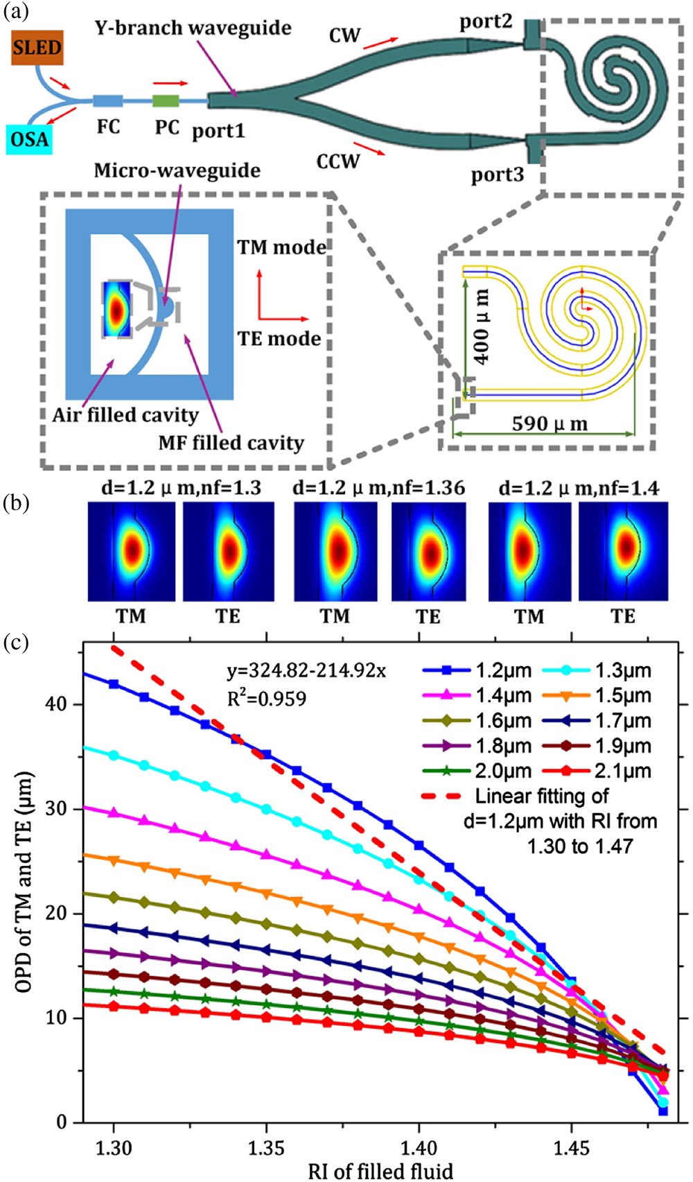
Figure 1.(a) Schematic diagram of the micro-SI magnetic field probe based on an SI sensor. (b) The guiding mode of D-shaped waveguide with the diameter of 1.2 μm and the analyte RI of 1.3, 1.36, and 1.4, respectively. (c) The simulation results about the effective OPD variation of the TM mode and TE mode of the D-shaped waveguide versus the fluid RI in the waveguide cavity with different waveguide diameters. SLED, superluminescent emitting diode; FC, fiber coupler; PC, polarization controller; CW, clockwise light; CCW, counterclockwise light.
It can be seen that the light from a superluminescent emitting diode (SLED) couples to port 1 of the Y-branch waveguide, and then it splits into two beams as clockwise (CW) and counterclockwise (CCW) lights. The CW and CCW lights couple into D-shaped waveguides on both ends of the MSOPS from the tapered waveguide, port 2, and port 3 of the Y-branches. There is a 45˚ angle between the incident polarization and the two modes of TM and TE in the D-shaped waveguide. Then the polarization can be divided into two polarizations as CW_TM and CW_TE with the intensities of Icw_TM and Icw_TE, respectively. Due to the birefringence of the D-shaped waveguide, the OPD of the two beams changes as the refractive index of the analyte changes. The D-shaped waveguide length of MSOPS from port 2, and port 3 is . Assuming that the RIs of the waveguide in the TM mode and TE mode are and , respectively, the OPD is when CW_TM and CW_TE propagate from port 2 to port 3. Due to the reciprocity of the optical path, when CCW_TM and CCW_TE propagate from port 3 to port 2, the OPD is same. So the birefringence of CW_TM and CW_TE can be expressed as
When the effective RI of the medium in the hollow cavity is changed, the FSR will be changed and the th attenuation dip will be shifted by the amount , estimated as
Hence, it is necessary to investigate the behavior and the relationship among the effective RIs of TM/TE modes, the waveguide diameter, and the analyte RI. In order to improve the sensitivity of the D-shaped waveguide to analytes, we design the diameter of the waveguide to be 1.2 μm. The average change rate of OPD between TE/TM modes over the entire waveguide length of with the liquid refractive index is 214.92 μm/RIU as the RI of analytes is from 1.3 to 1.47.
3. MAGNETIC FIELD PROBE FABRICATION
The proposed device is 3D printed on a fused glass substrate, and photoresist (IP-DIP, Nanoscribe) with a refractive index of 1.52 is used for fabrication. During the fabrication, a glass substrate is first cleaned by isopropanol and covered by a droplet of photoresist. A immersion lens is used to focus the femtosecond laser to write the structure directly on the substrate by a two-photon 3D printing system (Nanoscribe) as shown in Fig. 2(a). In the experiments, the laser power for writing is about 15 mW, and the writing speed is about 500 μm/s. Due to the device size being much larger and the spiral wavelength being only few micrometers, the device can be fragile during fabrication. Hence, the device was separated into several parts, and the spiral waveguide was wholly printed. To obtain better connection, the angle was set as 10°. Also, the writing speed is kept low to achieve a smooth surface and reduce transmission loss. It takes a few hours for fabrication, after which the device is developed by propylene glycol monomethyl ether acetate (PGMEA) and rinsed by isopropanol. Figure 2(b) shows the scanning electron microscopy (SEM) image of the printed SI device, and the inset shows the nano-waveguide with a diameter of 1.2 μm. It is clearly seen that the outer surface and the D-shaped waveguide are very smooth. It should be noted that the tapered waveguide is bent due to the electric discharge when performing the SEM, and this is not expected to occur in the actual fabricated sensors. The normalized reflection spectra of the micro-SI in air are obtained (shown below in this paper). The relative FSR of the device is calculated to be about 36.11 nm, which is confirmed by the simulation.
![]()
Figure 2.(a) The SI structure fabrication with direct laser writing on a substrate. (b) The microscope image and the SEM image of the SI device printed on a substrate.
After characterization, the 3D printed device is packaged as a magnetic field sensor as illustrated in Fig. 3. Here, an MF containing particles at nanoscale (Ferrotec Cor.) is used for filling into the hollow channel [Figs. 3(a) and 3(b)]. First, the two ends of the hollow channels without the waveguide are sealed using a UV adhesive with a refractive index of 1.527 (NOA61, Thorlabs), which is pumped by a syringe and an electronically controlled stage and then solidified by a UV source as shown in Fig. 3(c). This is used for keeping the cavity hollow. Second, the substrate with the device is fixed on another substrate, and an SMF tip is used for light coupling into the Y-branch port 1 as shown in Fig. 3(d). The fiber is glued when a maximal coupling is obtained. Next, the integrated device is put into a glass tube and is fixed using the UV curable adhesive as shown in Fig. 3(e). Before filling into the MF, the tube end with the guiding fiber is sealed. Lastly, the MF is filled into a syringe connecting a hollow fiber, which is controlled by an electronically controlled stage, and then with the help of a microscope system and a three-axis controlling system, the hollow fiber was carefully aligned to avoid touching the microstructure and slowly pulled out until the glass tube was filled with MF as shown in Fig. 3(f). Finally, the glass tube was covered by a small piece flat glass and sealed by the UV adhesive as illustrated in Figs. 3(g) and 3(h). Next, the fabricated device is experimentally characterized.
![]()
Figure 3.(a) MF under a magnet, UV adhesive, and syringe. (b) Schematic diagram for connecting and sealing the hollow fiber and syringe, and for filling the MF and adhesive into the syringe. (b') Schematic diagram for sealing one side of the gap between single-mode fiber and the glass tube. (c) Schematic diagram for sealing the two ponds of the SI structure with stages and microscope. (d) Schematic diagram for fixing the 3D-printed SI structure on a bigger substrate, focusing SMF to port 1 of Y-branch, and fixing the SMF on the bigger substrate. (e) Schematic diagram for taking the SI device into a glass tube and fixing it with UV adhesive. (f) Schematic diagram for filling MF into the glass tube with stages and microscope. (g) Schematic diagram for sealing the other side of magnetic field probe with UV adhesive and UV lamp. (h) The fabricated magnetic field probe.
4. EXPERIMENTS AND RESULTS
Figure 4(a) shows the schematic diagram of the magnetic field measurement setup where an SLED source ranging from 1350 to 1650 nm is used to guide the light to the sensor through an optical fiber circulator (OC), and the reflected light is recorded by an OSA (AQ6317B) with a minimum resolution of 10 pm. Here, the magnetic field is generated by a magnetic field generator with a stability of 0.001 Oe and an increment of 0.01 Oe from 0 to 300 Oe. The fabricated SI magnetic field probe is placed parallel at the center of the magnetic field, and a Gauss meter (F.W.BELL, 6010) is employed for reference. Figure 4(b) shows the normalized reflection spectra of the device with and without MF. It can be seen that the presence of MF does not cause any significant loss and is comparable to that of the device in air. The FSRs of the device with and without MF are 59.15 nm and 36.08 nm, respectively, which are consistent with the simulation results.
![]()
Figure 4.(a) Schematic diagram of the magnetic field probe measurement. SLED, superluminescent light emitting diode; OSA, optical spectrum analyzer; SMF, single-mode fiber; OC, optical fiber circulator. (b) The reflection spectra of the device in air and MF.
Figure 5(a) shows the experimental results of the proposed magnetic field sensor under a magnetic field from 0 to 100 Oe with an increment of 10 Oe. It clearly shows that the spectrum is blueshifted as the magnetic field increases. It should be noted that the index of the magnetic fluid increases and the effective indices of the two guiding modes, TM and TE, of the tapered waveguide increase as well when the magnetic field is applied. However, the effective index difference of the TM/TE modes decreases. In order to investigate the sensor performance in ultraweak magnetic field, Fig. 5(b) shows the experimental results under a weak magnetic field from 0 to 10 Oe. It can be seen that the change rates of the dip wavelengths with magnetic field from 0 to 100 Oe are larger than that from 0 to 10 Oe. The dip wavelength and peak-to-valley intensity around 1550 nm versus the magnetic field strength are plotted as shown in Fig. 5(c). The dip wavelength versus magnetic field can be classified into four areas as the figure shows. The dip wavelength slowly decreases in a nonlinear way as the magnetic field strength increases within a range from 0 to 10 Oe, which is called sluggish area (I). As the magnetic field strength increases from 10 to 100 Oe, the resonant wavelength is linearly blueshifted with a large slope, which means the device is very sensitive to the magnetic field in that range (II). The dip wavelength changed with magnetic field can be fitted linearly with a slope of 0.48 nm/Oe and with a fitting confidence of 0.9998. The resonant wavelength is allometric with the coefficient of 1592.41 and the power of as the magnetic field strength increases from 100 to 220 Oe, which is deemed as low-sensitivity area compared to area III as shown in Fig. 5(d). However, as the magnetic field increases to more than 220 Oe, it appears that the resonant wavelength does not change, and this is called the saturated area. Based on calculation, the magnetic field measurement accuracy is considering an OSA with a resolution of 10 pm.
![]()
Figure 5.(a), (b) Transmission spectral evolutions with an increasing applied magnetic field in the linear response region from 10 to 100 Oe and in the sluggish one from 0 to 10 Oe, respectively. (c) Variation of the fringe dip wavelength and peak-to-valley intensity with respect to an applied magnetic field. (d) Variation of the fringe dip wavelength with respect to an applied magnetic field in the sluggish area and low-sensitivity area.
The stability of the micro-SI probe to magnetic field within the linear range was next investigated. First, the direction of the magnetic field was studied. A magnetic field from 0 to 100 Oe is applied parallel to the SI device, and the interference spectra are recorded to compare with the data when the magnetic field is applied vertically. We found that there is no obvious difference when the magnetic field direction changes, indicating that the proposed device can only be used for scalar measurement. Next, the magnetic field was set to be vertical to the device, which was tested at a temperature of 20°C three times as the magnetic field increased from 0 to 100 Oe and further decreased to 0 Oe in steps of 10 Oe as shown in Fig. 6(a). It shows that the dip wavelength shifts linearly with the increase of the magnetic field. To make sure the MF is stable under each measurement, the spectra were recorded after the magnetic field was applied for a few minutes at different temperatures. The dip wavelength from 1460 to 1550 nm was tracked in each measurement under different magnetic fields at temperatures of 20°C, 30°C, and 40°C as shown in Fig. 6(b). The magnetic field sensor has a temperature sensitivity, which comes from the temperature sensitivity of the magnetic fluid and the thermal length expansion of the photoresist and can be compensated. Officially because of this sensitivity to temperature, this sensor can be used to sense temperature. The maximum dip wavelength errors at the test temperatures are calculated as 0.71, 0.86, and 0.96 nm for three repeated tests under different magnetic fields and at a temperature of 20°C, 30°C and 40°C, respectively. Next, the device’s long-term stability is investigated as shown in Fig. 6(c), where the dip wavelength fluctuations of the device under a magnetic field of 0, 50, and 100 Oe and within 72 h are recorded, and the maximum is about 0.72 nm, which contributes a magnetic field error of at a temperature of 20°C. The experimental result demonstrates that the response of the micro-SI structure is repeatedly stable to the applied magnetic field. Compared to the reported interferometer-based magnetic field sensors based on transmission in MF and modal coupling through lateral offset, tapering, or etching [22–26], the magnetic field sensor with micro-SI structure exhibits a very high magnetic field sensitivity.
![]()
Figure 6.(a) Repeated tests of the dip wavelength under different magnetic fields. (b) The dip wavelength at different magnetic field with temperature of 20°C, 30°C and 40°C, respectively, and the maximum dip wavelength errors for three repeated tests under different magnetic fields under 20°C, 30°C and 40°C, respectively. (c) The dip wavelength fluctuations within 72 h at a temperature of 20°C and under a magnetic field of 0, 50, and 100 Oe, respectively.
The response of the SI sensor to the magnetic field is also investigated, of which the experimental setup is shown in Fig. 7(a) where a tunable laser is used to choose the linear response area. The magnetic field sensor is placed at the center of Helmholtz coil, which is driven by a tunable current source. The current source can be controlled by a computer through a general-purpose interface bus (GPIB). The interference intensity of the SI device is detected by a photodetector (PD) and recorded by a data acquisition card. Here, a laser wavelength in the linear range of one resonant wavelength (near 1500 nm) is chosen for the light source. The output of the SI device versus time under a magnetic field is shown in Fig. 7(b). The response curves under different magnetic fields vary. The experimental results are consistent with the results in Fig. 5(a). The response times of the micro-SI device under different magnetic fields are studied as the left inset of Fig. 7(b) for applying magnetic field and the right inset of Fig. 7(b) for removing magnetic field. From the experimental results, it needs 3.1, 6.5, and 10.1 ms to response until the sensor is stable when applying a magnetic field of 2, 5, and 10 Oe. It needs similar time when removing the same magnetic field. It can be seen that the response time becomes longer as the magnetic field increases due to the magnetic particles clustering together. When the magnetic field is moving and the magnetic field is stronger, the gathering chain is longer and the releasing time increases. When the magnetic field is applied, the time to form the stable chain exhibits relatively the same behavior.
![]()
Figure 7.(a) Demonstration for measuring the response of SI to different magnetic fields. (b) The experimental results of response under different magnetic fields.
In order to further evaluate the magnetic field sensing performance of the proposed device, several typical reported sensors are compared and listed in Table 1. The table includes sensitivity, sensing range, and device size. The sensitivity of our device is highest except the result of Ref. [13], where a highly sensitive magnetic fluid is used. It should be noted that the used magnetic fluid is also an important factor on the sensing performance such as the sensitivity and the sensing range. However, from the perspective of the sensing principles, our proposed sensor is more sensitive than the reported sensor. Additionally, the 2PP technique enables to design highly sensitive micro- and nanodevices for sensing applications. Comparison of Magnetic Field Sensing Performance of Our Sensor and the Typical Reported SensorsSensitivity Sensing Range Size (W × L) Refs. 20.8 nm/mT 5–9.5 mT [ 0.073 nm/mT 10–40 mT [ 1.54 nm/mT 0–8 mT [ 0.115 nm/mT 2–14 mT [ 4.8 nm/mT 1–10 mT This study
5. CONCLUSION
In summary, we have experimentally demonstrated a two-photon 3D printed polymer-based micro-SI device on a substrate for magnetic field measurement with ultrahigh sensitivity. The effective optical path of micro-SI is 2.408 mm long with a D-shaped nano waveguide located at the center of a wall, which separates the cross surface of the muti-spiral SI into two cavities with one cavity full of air and the other cavity, including the D-shaped waveguide, filled by MF. The presence of the nano-waveguide can reduce significant transmission loss, enhance the evanescent coupling with MF, as well and lead to higher birefringence. It should be noted that the proposed device is very stable at different temperatures and under different magnetic fields; however, packaging of the sensor needs to be considered in view of the relative fragility of the 3D-printed device. Based on the experiments, the proposed magnetic field SI probe exhibits a sensitivity of 0.48 nm/Oe within a range from 10 to 100 Oe. The repeated experiments show that the fabricated device has a very high stability. The proposed 3D printed SI-based magnetic field probe is novel, robust, and stable, and it could be used for ultraweak magnetic field detection.
Acknowledgment
Acknowledgment. The authors thank the State Key Laboratory of Modern Optical Instrumentation, Zhejiang University, Zhejiang Lab, China, and also thank Key Laboratory of Specialty Fiber Optics and Optical Access Networks, Shanghai University for supporting this work. This work was performed using the facilities of the Center for Smart Structures and Materials at Northwestern University.
References
[1] M. Sadeghi, J. Sexton, C. Liang, M. Missous. Highly sensitive nanotesla quantum-well Hall-effect integrated circuit using GaAs–InGaAs–AlGaAs 2DEG. IEEE Sens. J., 15, 1817-1824(2015).
[2] K. Wang, Y. Zhang, G. Xiao. Anomalous Hall sensors with high sensitivity and stability based on interlayer exchange-coupled magnetic thin films. Phys. Rev. Appl., 13, 064009(2020).
[3] D. Collomb, P. Li, S. Bending. Nanoscale graphene Hall sensors for high-resolution ambient magnetic imaging. Sci. Rep., 9, 14424(2019).
[4] A. Manzin, V. Nabaei, R. Feerrero. Quantification of magnetic nanobeads with micrometer Hall sensors. IEEE Sens. J., 18, 10058-10065(2018).
[5] Z. Jiang, E. Burmistrov, V. Slobodchikov, V. Khanin, Y. Maslennikov, O. Snigirev. DC SQUID modulation electronics for operation with HTS DC SQUID magnetometers in the unshielded environment. IEEE Trans. Appl. Supercon., 19, 206-209(2009).
[6] P. Caputo, J. Oppenländer, C. Häussler, J. Tomes, A. Friesch, T. Träuble, N. Schopohl. High-performance magnetic field sensor based on superconducting quantum interference filters. Appl. Phys. Lett., 85, 1389-1391(2004).
[7] Z. Jiang, J. Dong, S. Hu, Y. Zhang, Y. Chen, Y. Luo, W. Zhu, W. Qiu, H. Lu, H. Guan, Y. Zhong, J. Yu, J. Zhang, Z. Chen. High-sensitivity vector magnetic field sensor based on side-polished fiber plasmon and ferrofluid. Opt. Lett., 43, 4743-4746(2018).
[8] N. Abdukerim, D. Grobnic, C. Hnatovsky, S. Mihailov. Through-the-coating writing of tilted fiber Bragg gratings with the phase mask technique. Opt. Express, 27, 38259-38269(2019).
[9] Z. Di, X. Chen, S. Pu, X. Hu, Y. Xia. Magnetic-field-induced birefringence and particle agglomeration in magnetic fluids. Appl. Phys. Lett., 89, 211106(2006).
[10] J. Li, X. Liu, Y. Lin, L. Bai, Q. Li, X. Chen. Field modulation of light transmission through ferrofluid film. Appl. Phys. Lett., 91, 253108(2007).
[11] P. Zu, C. Chan, G. Koh, W. Lew, Y. Jin, H. Liew, W. Wong, X. Dong. Enhancement of the sensitivity of magneto-optical fiber sensor by magnifying the birefringence of magnetic fluid film with Loyt-Sagnac interferometer. Sens. Actuators B, 191, 19-23(2014).
[12] M. Deng, X. Sun, M. Han, D. Li. Compact magnetic-field sensor based on optical microfiber Michelson interferometer and Fe3O4 nanofluid. Appl. Opt., 52, 734-741(2013).
[13] Z. Li, C. Liao, J. Song, Y. Wang, F. Zhu, Y. Wang, X. Dong. Ultrasensitive magnetic field sensor based on an in-fiber Mach–Zehnder interferometer with a magnetic fluid component. Photon. Res., 4, 197-201(2016).
[14] J. Yin, S. Ruan, T. Liu, J. Jiang, S. Wang, H. Wei, P. Yan. All-fiber-optic vector magnetometer based on nano-magnetic fluids filled double-clad photonic crystal fiber. Sens. Actuators B, 238, 518-524(2017).
[15] Y. Zhao, D. Wu, R. Lv, J. Li. Magnetic field measurement based on the Sagnac interferometer with a ferrofluid-filled high-birefringence photonic crystal fiber. IEEE Trans. Instrum. Meas., 65, 1503-1507(2016).
[16] D. Zhang, H. Wei, S. Krishnaswamy. Highly sensitive magnetic field microsensor based on direct laser writing of fiber-tip optofluidic Fabry-Perot cavity. APL Photon., 5, 076112(2020).
[17] W. Wang, Y. Miao, Z. Li, H. Zhang, B. Li, X. Yang, J. Yao. Tunability of Hi-Bi photonic crystal fiber integrated with selectively filled magnetic fluid and microfluidic manipulation. Appl. Opt., 58, 979-983(2019).
[18] L. Gao, T. Zhu, M. Deng, K. Chiang, X. Sun, X. Dong, Y. Hou. Long-period fiber grating within D-shaped fiber using magnetic fluid for magnetic-field detection. IEEE Photon. J., 4, 2095-2104(2012).
[19] Y. Dong, B. Wu, M. Wang, H. Xiao, S. Xiao, C. Sun, H. Li, S. Jian. Magnetic field and temperature sensor based on D-shaped fiber modal interferometer and magnetic fluid. Opt. Laser Technol., 107, 169-173(2018).
[20] J. Tian, Y. Zuo, M. Hou, Y. Jiang. Magnetic field measurement based on a fiber laser oscillation circuit merged with a polarization-maintaining fiber Sagnac interference structure. Opt. Express, 29, 8763-8769(2021).
[21] H. Wei, S. Krishnaswamy. Polymer micro-ring resonator integrated with a fiber ring laser for ultrasound detection. Opt. Lett., 42, 2655-2658(2017).
[22] Y. Zhao, R. Lv, D. Wang, Q. Wang. Fiber optic Fabry-Perot magnetic field sensor with temperature compensation using a fiber Bragg grating. IEEE Trans. Instrum. Meas., 63, 2210-2214(2014).
[23] X. Li, Y. Zhao, L. Cai, X. Zhou. Measurement of magnetic field and temperature based on fiber-optic composite interferometer. IEEE T. Instrum. Meas., 66, 1906-1911(2017).
[24] S. Dong, S. Pu, H. Wang. Magnetic field sensing based on magnetic-fluid-clad fiber-optic structure with taper-like and lateral- offset fusion splicing. Opt. Express, 22, 19108-19116(2014).
[25] Y. Chen, T. Liu, Q. Han, W. Yan, L. Yu. Fiber loop ring-down cavity integrated U-bent single-mode-fiber for magnetic field sensing. Photon. Res., 4, 322-326(2016).
[26] X. Zhou, X. Li, S. Li, G. An, T. Cheng. Magnetic field sensing based on SPR optical fiber sensor interacting with magnetic fluid. IEEE Trans. Instrum. Meas., 68, 234-239(2019).

Set citation alerts for the article
Please enter your email address
© Copyright 2018-2021 | Chinese Laser Press. All Rights Reserved 沪ICP备15018463号-20