• Advanced Photonics
  • Vol. 3, Issue 3, 034002 (2021)
Zhiping Hu1, Zhengzheng Liu2, Zijun Zhan1, Tongchao Shi2, Juan Du1、2、*, Xiaosheng Tang3、4、*, and Yuxin Leng1、2、*
Author Affiliations
  • 1University of Chinese Academy of Sciences, Hangzhou Institute for Advanced Study, Hangzhou, China
  • 2Chinese Academy of Sciences, Shanghai Institute of Optics and Fine Mechanics, State Key Laboratory of High Field Laser Physics and CAS Center for Excellence in Ultra-Intense Laser Science, Shanghai, China
  • 3Chongqing University of Posts and Telecommunications, School of Optoelectronic Engineering, Chongqing, China
  • 4Zhengzhou University, School of Materials Science and Engineering, Zhengzhou, China
  • show less
    DOI: 10.1117/1.AP.3.3.034002 Cite this Article Set citation alerts
    Zhiping Hu, Zhengzheng Liu, Zijun Zhan, Tongchao Shi, Juan Du, Xiaosheng Tang, Yuxin Leng. Advances in metal halide perovskite lasers: synthetic strategies, morphology control, and lasing emission[J]. Advanced Photonics, 2021, 3(3): 034002 Copy Citation Text show less
    (a) Structural model of metal lead perovskites. Figures reproduced from Ref. 43. (b) The (t,μ) map for 138 perovskite compounds. Figures reproduced from Ref. 44. (c) Nanoscale morphologies of halide perovskites.
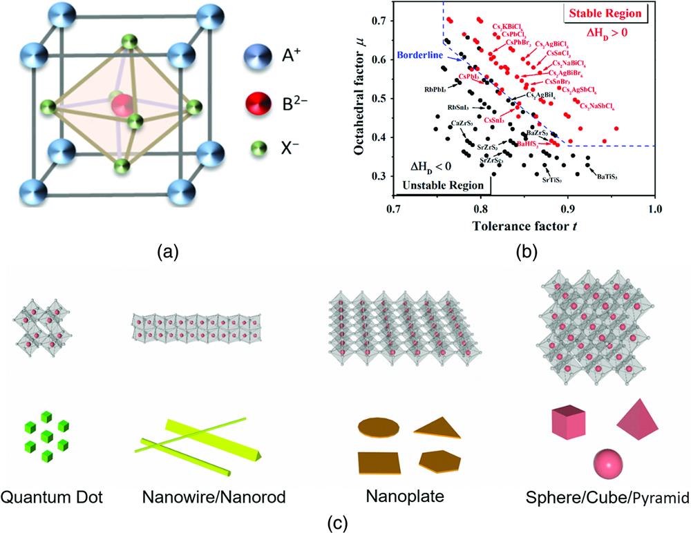
    Fig. 1. (a) Structural model of metal lead perovskites. Figures reproduced from Ref. 43. (b) The (t,μ) map for 138 perovskite compounds. Figures reproduced from Ref. 44. (c) Nanoscale morphologies of halide perovskites.
    (a) Schematic of LARP technique. Figures reproduced from Ref. 25. (b) Schematic of precursor and optical image of MAPbBr3 solution. Figures reproduced from Ref. 25. (c) Optical images of MAPbX3 solution under natural light and under 365 nm excitation. Figures reproduced from Ref. 25. (d) PL spectra of MAPbX3 QDs. Figures reproduced from Ref. 25. (e) PL optical images and PL spectra of CsPbX3 QDs. Figures reproduced from Ref. 42. (f) Time-resolved PL decays for CsPbX3 QDs. Figures reproduced from Ref. 42. (g) Schematic of the anion-exchange of CsPbX3. Figures reproduced from Ref. 41. (h) TEM images of CsPbX3 QDs with various PL. Figures reproduced from Ref. 41. (i) Schematic of room-temperature fabrication of CsPbX3 QDs. Figures reproduced from Ref. 39. (j) Optical images of CsPbX3 QDs after the addition of precursor ion solutions for 3 s. Figures reproduced from Ref. 39.
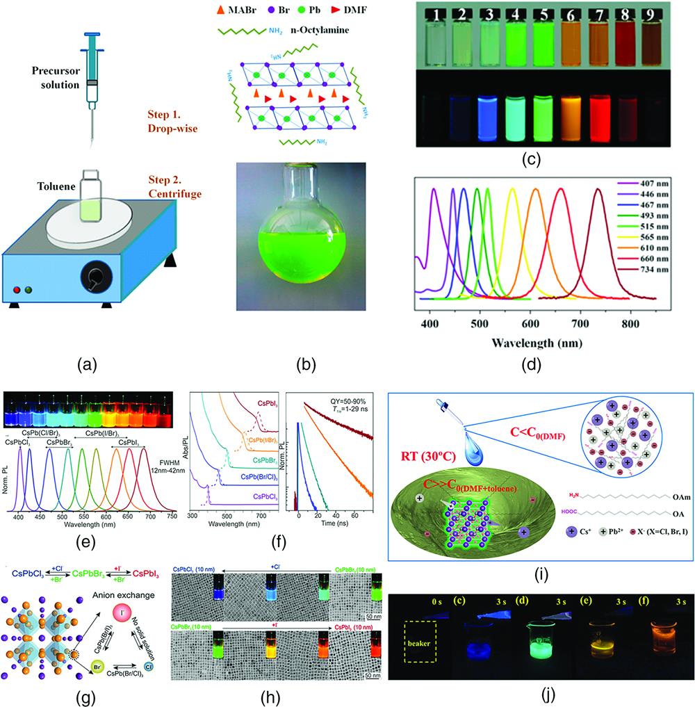
    Fig. 2. (a) Schematic of LARP technique. Figures reproduced from Ref. 25. (b) Schematic of precursor and optical image of MAPbBr3 solution. Figures reproduced from Ref. 25. (c) Optical images of MAPbX3 solution under natural light and under 365 nm excitation. Figures reproduced from Ref. 25. (d) PL spectra of MAPbX3 QDs. Figures reproduced from Ref. 25. (e) PL optical images and PL spectra of CsPbX3 QDs. Figures reproduced from Ref. 42. (f) Time-resolved PL decays for CsPbX3 QDs. Figures reproduced from Ref. 42. (g) Schematic of the anion-exchange of CsPbX3. Figures reproduced from Ref. 41. (h) TEM images of CsPbX3 QDs with various PL. Figures reproduced from Ref. 41. (i) Schematic of room-temperature fabrication of CsPbX3 QDs. Figures reproduced from Ref. 39. (j) Optical images of CsPbX3 QDs after the addition of precursor ion solutions for 3 s. Figures reproduced from Ref. 39.
    (a) Schematic of the fabrication process for the Csx(CH3NH3)1−xPbI3 NWs. Figures reproduced from Ref. 72. (b) Schematic of the formation of the MAPbI3 NWs by recrystallization process. Figures reproduced from Ref. 73. (c) TEM images of as-grown CsPbBr3 NCs with increasing times. Figures reproduced from Ref. 51. (d) Absorption and PL spectra of CsPbBr3 NWs. Figures reproduced from Ref. 56. (e) Schematic of the passivation effect by HX on the length of CsPbX3 NWs and TEM images of the synthesized CsPbX3 NWs. Figures reproduced from Ref. 58. (f) Normalized absorption, PL spectra, and photographs of CsPbX3 NWs. Figures reproduced from Ref. 58.
    Fig. 3. (a) Schematic of the fabrication process for the Csx(CH3NH3)1xPbI3 NWs. Figures reproduced from Ref. 72. (b) Schematic of the formation of the MAPbI3 NWs by recrystallization process. Figures reproduced from Ref. 73. (c) TEM images of as-grown CsPbBr3 NCs with increasing times. Figures reproduced from Ref. 51. (d) Absorption and PL spectra of CsPbBr3 NWs. Figures reproduced from Ref. 56. (e) Schematic of the passivation effect by HX on the length of CsPbX3 NWs and TEM images of the synthesized CsPbX3 NWs. Figures reproduced from Ref. 58. (f) Normalized absorption, PL spectra, and photographs of CsPbX3 NWs. Figures reproduced from Ref. 58.
    (a) SEM image of PbI2 NWs. Figures reproduced from Ref. 49. (b) Optical microscopy image of MAPbI3 NWs. Figures reproduced from Ref. 49. Structure simulation images of (c) PbI2 NW and (d) MAPbI3 NW. Figures reproduced from Ref. 49. (e) Schematic of the CsPbX3 triangular micro/NRs. Figures reproduced from Ref. 75. (f) SEM image of CsPbBr3 triangular rods. Figures reproduced from Ref. 75. (g) Real-color image and PL spectra of CsPbX3 triangular rods. Figures reproduced from Ref. 75. (h), (i) SEM images of the CsPbBr3 NWs. Figures reproduced from Ref. 62.
    Fig. 4. (a) SEM image of PbI2 NWs. Figures reproduced from Ref. 49. (b) Optical microscopy image of MAPbI3 NWs. Figures reproduced from Ref. 49. Structure simulation images of (c) PbI2 NW and (d) MAPbI3 NW. Figures reproduced from Ref. 49. (e) Schematic of the CsPbX3 triangular micro/NRs. Figures reproduced from Ref. 75. (f) SEM image of CsPbBr3 triangular rods. Figures reproduced from Ref. 75. (g) Real-color image and PL spectra of CsPbX3 triangular rods. Figures reproduced from Ref. 75. (h), (i) SEM images of the CsPbBr3 NWs. Figures reproduced from Ref. 62.
    (a) Schematic of the synthesis of MAPbBr3 NPs. Figures reproduced from Ref. 61. (b) Quantum size effect in MAPbBr3 NPs. Figures reproduced from Ref. 61. (c) Bandgap tuning in MAPbBr3 NPs and micro/NRs via size or compositional control. Figures reproduced from Ref. 61. (d) PL spectra of the halide–anion exchanged CsPbX3 NPs. Figures reproduced from Ref. 37. (e) 2D CsPbBr3 NSs. Figures reproduced from Ref. 37. (f) SEM images of CsPb2Br5 MP. Figures reproduced from Ref. 78. (g) Top: Schematic of the growth of 2D CsPbX3 NPs and NSs from CsPbX3 NRs. Bottom: TEM images of CsPbBr3 NCs for different times. Figures reproduced from Ref. 79. (h) Schematic of the fabrication of MAPbI3 NCs using a vapor-transport system. Figures reproduced from Ref. 80. (i) Thickness of PbI2 platelets before and after being converted to MAPbI3. Figures reproduced from Ref. 80. (j) Optical images of as-grown MAPbI3 NCs with different temperature and pressure. Figures reproduced from Ref. 64.
    Fig. 5. (a) Schematic of the synthesis of MAPbBr3 NPs. Figures reproduced from Ref. 61. (b) Quantum size effect in MAPbBr3 NPs. Figures reproduced from Ref. 61. (c) Bandgap tuning in MAPbBr3 NPs and micro/NRs via size or compositional control. Figures reproduced from Ref. 61. (d) PL spectra of the halide–anion exchanged CsPbX3 NPs. Figures reproduced from Ref. 37. (e) 2D CsPbBr3 NSs. Figures reproduced from Ref. 37. (f) SEM images of CsPb2Br5 MP. Figures reproduced from Ref. 78. (g) Top: Schematic of the growth of 2D CsPbX3 NPs and NSs from CsPbX3 NRs. Bottom: TEM images of CsPbBr3 NCs for different times. Figures reproduced from Ref. 79. (h) Schematic of the fabrication of MAPbI3 NCs using a vapor-transport system. Figures reproduced from Ref. 80. (i) Thickness of PbI2 platelets before and after being converted to MAPbI3. Figures reproduced from Ref. 80. (j) Optical images of as-grown MAPbI3 NCs with different temperature and pressure. Figures reproduced from Ref. 64.
    (a) Perovskite metasurfaces with enhanced emission. Figures reproduced from Ref. 98. SEM images of perovskite with (b) nanostripe and (c) nanohole structures. Figures reproduced from Ref. 98. (d) Enhanced PL spectra from perovskite metasurfaces with different structures. Figures reproduced from Ref. 98. (e) Schematics of the polymer-assisted nanoimprinting process for perovskite nanopatterns. Figures reproduced from Ref. 94. (f) SEM images of various perovskite nanopatterns. Figures reproduced from Ref. 94. (g) SEM images of MAPbBr3 metasurface for nonlinear imaging. Figures reproduced from Ref. 90. (h) The nonlinear PL and linear PL images of MAPbBr3 metasurfaces. Figures reproduced from Ref. 90. (i) SEM image of MAPbBr3 metasurface. Figures reproduced from Ref. 96. (j) The field distributions of MAPbBr3 perovskite metasurface. Figures reproduced from Ref. 96.
    Fig. 6. (a) Perovskite metasurfaces with enhanced emission. Figures reproduced from Ref. 98. SEM images of perovskite with (b) nanostripe and (c) nanohole structures. Figures reproduced from Ref. 98. (d) Enhanced PL spectra from perovskite metasurfaces with different structures. Figures reproduced from Ref. 98. (e) Schematics of the polymer-assisted nanoimprinting process for perovskite nanopatterns. Figures reproduced from Ref. 94. (f) SEM images of various perovskite nanopatterns. Figures reproduced from Ref. 94. (g) SEM images of MAPbBr3 metasurface for nonlinear imaging. Figures reproduced from Ref. 90. (h) The nonlinear PL and linear PL images of MAPbBr3 metasurfaces. Figures reproduced from Ref. 90. (i) SEM image of MAPbBr3 metasurface. Figures reproduced from Ref. 96. (j) The field distributions of MAPbBr3 perovskite metasurface. Figures reproduced from Ref. 96.
    (a) SEM image of the CsPbI3 MSs. Figures reproduced from Ref. 100. (b) PL spectra of CsPbCl3, CsPbBr3, and CsPbI3 MSs. Figures reproduced from Ref. 100. (c) Monodispersed CsPbBr3 spheres under the excitation of UV light. Figures reproduced from Ref. 101. (d) SEM image of the monodispersed CsPbBr3 spheres. Figures reproduced from Ref. 101. (e) SEM image of the MAPbBr3 triangular pyramids. Figures reproduced from Ref. 102. (f) SEM image of the CsPbI3 triangular pyramids on a Si/SiO2 substrate. Figures reproduced from Ref. 103. (g) SEM image and (h) schematic of the formation of CsPbX3 nanoflowers. Figures reproduced from Ref. 104. (i) Photograph (upper) and PL emission spectra (bottom) of CsPbX3 nanoflowers. Figures reproduced from Ref. 104. (j) Crystal growth of MAPbBr3 cuboids (top) and SEM images of MAPbBr3 perovskite under different reaction time (bottom). Figures reproduced from Ref. 105.
    Fig. 7. (a) SEM image of the CsPbI3 MSs. Figures reproduced from Ref. 100. (b) PL spectra of CsPbCl3, CsPbBr3, and CsPbI3 MSs. Figures reproduced from Ref. 100. (c) Monodispersed CsPbBr3 spheres under the excitation of UV light. Figures reproduced from Ref. 101. (d) SEM image of the monodispersed CsPbBr3 spheres. Figures reproduced from Ref. 101. (e) SEM image of the MAPbBr3 triangular pyramids. Figures reproduced from Ref. 102. (f) SEM image of the CsPbI3 triangular pyramids on a Si/SiO2 substrate. Figures reproduced from Ref. 103. (g) SEM image and (h) schematic of the formation of CsPbX3 nanoflowers. Figures reproduced from Ref. 104. (i) Photograph (upper) and PL emission spectra (bottom) of CsPbX3 nanoflowers. Figures reproduced from Ref. 104. (j) Crystal growth of MAPbBr3 cuboids (top) and SEM images of MAPbBr3 perovskite under different reaction time (bottom). Figures reproduced from Ref. 105.
    (a) Absorption spectrum and normalized two-photon PL spectra of single MAPbBr3 NCs. Figures reproduced from Ref. 115. (b) Schematic of two-photon absorption at 800 nm in perovskite. Figures reproduced from Ref. 115. (c) Two-photon absorption coefficient. (d) Inverse transmission versus peak intensity for typical single MAPbBr3 NCs. Figures reproduced from Ref. 115. (e)–(g) Nonlinear optics of CsPbX3 NCs: (e) linear absorption spectrum and normalized PL spectra from CsPbBr3 NCs, (f) PL decay of CsPbBr3 NCs, and (g) Z-scan responses of the CsPbBr3 NC solution and the pure solvent. Figures reproduced from Ref. 116.
    Fig. 8. (a) Absorption spectrum and normalized two-photon PL spectra of single MAPbBr3 NCs. Figures reproduced from Ref. 115. (b) Schematic of two-photon absorption at 800 nm in perovskite. Figures reproduced from Ref. 115. (c) Two-photon absorption coefficient. (d) Inverse transmission versus peak intensity for typical single MAPbBr3 NCs. Figures reproduced from Ref. 115. (e)–(g) Nonlinear optics of CsPbX3 NCs: (e) linear absorption spectrum and normalized PL spectra from CsPbBr3 NCs, (f) PL decay of CsPbBr3 NCs, and (g) Z-scan responses of the CsPbBr3 NC solution and the pure solvent. Figures reproduced from Ref. 116.
    (a) TEM images of CsPbBr3 QDs. Figures reproduced from Ref. 127. (b) Spectral tunability of ASE of CsPbX3 via compositional modulation. Figures reproduced from Ref. 127. (c) Evolution from PL to lasing in an MS resonator with increasing pump intensity. Figures reproduced from Ref. 127. (d) SEM image and (e) isolation effect of CsPbBr3QDs/A-SiO2 composites. Figures reproduced from Ref. 131. (f) PL spectra from CsPbBr3QDs/A-SiO2 composite with increasing pump intensity. Figures reproduced from Ref. 131. (g) TEM image of FAPbBr3 QDs. (h) Two-photon PL spectra from FAPbBr3 NCs in a microcapillary tube. (i) Optical image and (j) lasing emission spectra from FAPbBr3 NCs in a microcapillary tube. Figures reproduced from Ref. 132. (k) Left: PL spectra from CsPbBr3 film within/without microcavity. Right: Schematic of the CsPbBr3 VCSEL. Figures reproduced from Ref. 133. (l) Schematic of the CsPbBr3 VCSEL. Figures reproduced from Ref. 134. (m) Photograph and PL stability of flexible FAPbBr3 VCSEL. Figures reproduced from Ref. 135.
    Fig. 9. (a) TEM images of CsPbBr3 QDs. Figures reproduced from Ref. 127. (b) Spectral tunability of ASE of CsPbX3 via compositional modulation. Figures reproduced from Ref. 127. (c) Evolution from PL to lasing in an MS resonator with increasing pump intensity. Figures reproduced from Ref. 127. (d) SEM image and (e) isolation effect of CsPbBr3QDs/A-SiO2 composites. Figures reproduced from Ref. 131. (f) PL spectra from CsPbBr3QDs/A-SiO2 composite with increasing pump intensity. Figures reproduced from Ref. 131. (g) TEM image of FAPbBr3 QDs. (h) Two-photon PL spectra from FAPbBr3 NCs in a microcapillary tube. (i) Optical image and (j) lasing emission spectra from FAPbBr3 NCs in a microcapillary tube. Figures reproduced from Ref. 132. (k) Left: PL spectra from CsPbBr3 film within/without microcavity. Right: Schematic of the CsPbBr3 VCSEL. Figures reproduced from Ref. 133. (l) Schematic of the CsPbBr3 VCSEL. Figures reproduced from Ref. 134. (m) Photograph and PL stability of flexible FAPbBr3 VCSEL. Figures reproduced from Ref. 135.
    (a) SEM of MAPbI3 nanostructures. Figures reproduced from Ref. 144. (b) Optical image of single MAPbI3 NW. Figures reproduced from Ref. 144. (c) PL spectra of MAPbI3 NW around the lasing threshold. Figures reproduced from Ref. 144. (d) Broad tunable lasing from single-crystal MAPbX3 NW. Figures reproduced from Ref. 144. (e) SEM image of CsPbBr3 nanostructures. Figures reproduced from Ref. 145. (f) Fluorescence images of red/green/blue CsPbX3 NWs above lasing threshold. Figures reproduced from Ref. 145. (g) Broad tunable lasing from single-crystal CsPbX3 NWs. Figures reproduced from Ref. 145. (h) The photograph and PL spectra of a single CsPbCl3−3xBr3x NW. Figures reproduced from Ref. 146. (i) The schematic of optically pumping lasing from a single CsPbCl3−3xBr3x NW. Figures reproduced from Ref. 146. (j) Typical lasing spectra from a single CsPbCl3−3xBr3x NW. Figures reproduced from Ref. 146.
    Fig. 10. (a) SEM of MAPbI3 nanostructures. Figures reproduced from Ref. 144. (b) Optical image of single MAPbI3 NW. Figures reproduced from Ref. 144. (c) PL spectra of MAPbI3 NW around the lasing threshold. Figures reproduced from Ref. 144. (d) Broad tunable lasing from single-crystal MAPbX3 NW. Figures reproduced from Ref. 144. (e) SEM image of CsPbBr3 nanostructures. Figures reproduced from Ref. 145. (f) Fluorescence images of red/green/blue CsPbX3 NWs above lasing threshold. Figures reproduced from Ref. 145. (g) Broad tunable lasing from single-crystal CsPbX3 NWs. Figures reproduced from Ref. 145. (h) The photograph and PL spectra of a single CsPbCl33xBr3x NW. Figures reproduced from Ref. 146. (i) The schematic of optically pumping lasing from a single CsPbCl33xBr3x NW. Figures reproduced from Ref. 146. (j) Typical lasing spectra from a single CsPbCl33xBr3x NW. Figures reproduced from Ref. 146.
    (a) Schematic of an MAPbX3 NP pumped by a pulsed laser. Figures reproduced from Ref. 80. (b) Optical image of MAPbI3 NPs under white light and laser excitation. Figures reproduced from Ref. 80. (c) Lasing spectra of hexagonal MAPbI3 NPs (upper) and the lasing mode evaluation with pumping fluence (bottom). Figures reproduced from Ref. 80. (d) Upper: Lasing spectra of triangular MAPbI3 NPs with different edge length. Bottom: The wavelength of lasing modes and Q-factor as a function of the triangular cavity edge length. Figures reproduced from Ref. 80. (e) Schematic of triangular MAPbI3 NPs pumped by a 343 nm laser. Figures reproduced from Ref. 148. (f) Optical image of triangular MAPbI3 NPs. Figures reproduced from Ref. 148. (g) 2D plot of a triangular MAPbI3 NP emission under different pump densities. Figures reproduced from Ref. 148. (h) The emission spectra from MAPbI3 NPs around the lasing threshold. Figures reproduced from Ref. 148. (i) Output emission intensity as a function of pump densities. Figures reproduced from Ref. 148. (j) Schematic of a CsPbX3 plate under a 400 nm laser. Figures reproduced from Ref. 149. (k) Emission spectra at different pump intensities. Figures reproduced from Ref. 149. (l) Tunable lasing spectra and images of individual CsPbX3 perovskite NPs. Figures reproduced from Ref. 149. (m) Single-mode lasing of CsPbBrxI3−x. Figures reproduced from Ref. 149. (n) Schematic of a CsPbI3 NS on mica substrate. Figures reproduced from Ref. 86. Excitation intensity-dependent emission spectra under (o) 470 nm and (p) 1200 nm excitation. Figures reproduced from Ref. 86. (q) Gaussian fitting of a lasing mode under 470 and 1200 nm laser. Figures reproduced from Ref. 86.
    Fig. 11. (a) Schematic of an MAPbX3 NP pumped by a pulsed laser. Figures reproduced from Ref. 80. (b) Optical image of MAPbI3 NPs under white light and laser excitation. Figures reproduced from Ref. 80. (c) Lasing spectra of hexagonal MAPbI3 NPs (upper) and the lasing mode evaluation with pumping fluence (bottom). Figures reproduced from Ref. 80. (d) Upper: Lasing spectra of triangular MAPbI3 NPs with different edge length. Bottom: The wavelength of lasing modes and Q-factor as a function of the triangular cavity edge length. Figures reproduced from Ref. 80. (e) Schematic of triangular MAPbI3 NPs pumped by a 343 nm laser. Figures reproduced from Ref. 148. (f) Optical image of triangular MAPbI3 NPs. Figures reproduced from Ref. 148. (g) 2D plot of a triangular MAPbI3 NP emission under different pump densities. Figures reproduced from Ref. 148. (h) The emission spectra from MAPbI3 NPs around the lasing threshold. Figures reproduced from Ref. 148. (i) Output emission intensity as a function of pump densities. Figures reproduced from Ref. 148. (j) Schematic of a CsPbX3 plate under a 400 nm laser. Figures reproduced from Ref. 149. (k) Emission spectra at different pump intensities. Figures reproduced from Ref. 149. (l) Tunable lasing spectra and images of individual CsPbX3 perovskite NPs. Figures reproduced from Ref. 149. (m) Single-mode lasing of CsPbBrxI3x. Figures reproduced from Ref. 149. (n) Schematic of a CsPbI3 NS on mica substrate. Figures reproduced from Ref. 86. Excitation intensity-dependent emission spectra under (o) 470 nm and (p) 1200 nm excitation. Figures reproduced from Ref. 86. (q) Gaussian fitting of a lasing mode under 470 and 1200 nm laser. Figures reproduced from Ref. 86.
    (a) Schematic of a single CsPbBr3 MS under 400 nm laser. Figures reproduced from Ref. 100. (b) Lasing PL spectra from a single CsPbBr3 MS under different pump intensities. Figures reproduced from Ref. 100. (c) Lorentzian fitting of a lasing mode. Figures reproduced from Ref. 100. (d) Photograph and lasing emission of multicolor CsPbX3 MS lasers. Figures reproduced from Ref. 100. (e) SEM image and (f) schematics of F-P cavity of CsPbBr3 nanocuboids. Figures reproduced from Ref. 129. (g) Single-mode lasing spectra and (h) TA spectroscopic data of CsPbBr3 nanocuboids under two-photon excitation. Figures reproduced from Ref. 129. (i) Schematic of a cube-corner MAPbBr3 pyramid under 405 nm laser. Figures reproduced from Ref. 102. (j) PL spectra of a cube-corner MAPbBr3 and (k) output intensity as a function of excitation power. Figures reproduced from Ref. 102. (l), (m) Multimode lasing spectra of a cube-corner pyramid of MAPbBr3 on (l) mica and (m) mica/Ag. Figures reproduced from Ref. 102.
    Fig. 12. (a) Schematic of a single CsPbBr3 MS under 400 nm laser. Figures reproduced from Ref. 100. (b) Lasing PL spectra from a single CsPbBr3 MS under different pump intensities. Figures reproduced from Ref. 100. (c) Lorentzian fitting of a lasing mode. Figures reproduced from Ref. 100. (d) Photograph and lasing emission of multicolor CsPbX3 MS lasers. Figures reproduced from Ref. 100. (e) SEM image and (f) schematics of F-P cavity of CsPbBr3 nanocuboids. Figures reproduced from Ref. 129. (g) Single-mode lasing spectra and (h) TA spectroscopic data of CsPbBr3 nanocuboids under two-photon excitation. Figures reproduced from Ref. 129. (i) Schematic of a cube-corner MAPbBr3 pyramid under 405 nm laser. Figures reproduced from Ref. 102. (j) PL spectra of a cube-corner MAPbBr3 and (k) output intensity as a function of excitation power. Figures reproduced from Ref. 102. (l), (m) Multimode lasing spectra of a cube-corner pyramid of MAPbBr3 on (l) mica and (m) mica/Ag. Figures reproduced from Ref. 102.
    (a) SEM image of the MAPbBr3 microwire on silicon grating. Figures reproduced from Ref. 156. (b) Laser spectrum of MAPbBr3 microwire. Figures reproduced from Ref. 156. (c) Optical image of MAPbBr3 NW arrays. Figures reproduced from Ref. 157. (d) PL spectra of a single MAPbBr3 NW under 400 nm laser. Figures reproduced from Ref. 157. (e) “LASER” patterned perovskite square MPs. Figures reproduced from Ref. 158. (f) Lasing spectra from perovskite MPs with different sizes. Figures reproduced from Ref. 158. (g) PL image of green and red QD arrays. Figures reproduced from Ref. 159. (h) Emission intensity versus excitation fluence measured from a CsPbBr3 MD. Figures reproduced from Ref. 159. (i) Lasing spectra from CsPbBr3 MDs with different diameters. Figures reproduced from Ref. 159. (j) PL spectra from a typical MAPbBr3 MD with different power energies and (k) output intensity and FWHM as a function of pump intensity. Figures reproduced from Ref. 160. (l) Widely tunable lasing from MAPbX3 arrays. Figures reproduced from Ref. 160. (m) Left: SEM image of the fabricated perovskite metasurface; right: ultrafast control of the quasi-BIC microlasers. Figures reproduced from Ref. 161.
    Fig. 13. (a) SEM image of the MAPbBr3 microwire on silicon grating. Figures reproduced from Ref. 156. (b) Laser spectrum of MAPbBr3 microwire. Figures reproduced from Ref. 156. (c) Optical image of MAPbBr3 NW arrays. Figures reproduced from Ref. 157. (d) PL spectra of a single MAPbBr3 NW under 400 nm laser. Figures reproduced from Ref. 157. (e) “LASER” patterned perovskite square MPs. Figures reproduced from Ref. 158. (f) Lasing spectra from perovskite MPs with different sizes. Figures reproduced from Ref. 158. (g) PL image of green and red QD arrays. Figures reproduced from Ref. 159. (h) Emission intensity versus excitation fluence measured from a CsPbBr3 MD. Figures reproduced from Ref. 159. (i) Lasing spectra from CsPbBr3 MDs with different diameters. Figures reproduced from Ref. 159. (j) PL spectra from a typical MAPbBr3 MD with different power energies and (k) output intensity and FWHM as a function of pump intensity. Figures reproduced from Ref. 160. (l) Widely tunable lasing from MAPbX3 arrays. Figures reproduced from Ref. 160. (m) Left: SEM image of the fabricated perovskite metasurface; right: ultrafast control of the quasi-BIC microlasers. Figures reproduced from Ref. 161.
    (a) Field intensity distributions and schematic structure of Ag/PMMA/perovskite. Figures reproduced from Ref. 163. (b) Schematic and working process of plasmonic nanolaser of MAPbBr3/Al2O3/TiN. Figures reproduced from Ref. 164. (c) Schematic and calculated electric field distribution of plasmonic nanolaser based on CsPbBr3 QDs. Figures reproduced from Ref. 165. (d) Schematic of phase transition from polycrystalline to monocrystalline CsPbBr3 nanoparticles by adjusting the laser power and the PL spectrum under different laser power. Figures reproduced from Ref. 166. (e) Schematic polaritons in a micro/NW cavity and lasing spectrum of CsPbBr3 NWs. Figures reproduced from Ref. 167. (f) Schematic of CW lasing of CsPbBr3 nanoribbons. Figures reproduced from Ref. 168. (g) Schematic structure of CsPbBr3 flakes/DBR microcavity and SEM image of CsPbBr3 flakes. Figures reproduced from Ref. 169. (h) Cascade energy transfer in quasi-2D perovskite and tunable ASE from solution-processed (NMA)2(FA)Pb2BryI7−y films. Figures reproduced from Ref. 170. (i) Chemical structures of quasi-2D perovskite with different organic cations and CW lasing characteristics of quasi-2D perovskite films. Figures reproduced from Ref. 171.
    Fig. 14. (a) Field intensity distributions and schematic structure of Ag/PMMA/perovskite. Figures reproduced from Ref. 163. (b) Schematic and working process of plasmonic nanolaser of MAPbBr3/Al2O3/TiN. Figures reproduced from Ref. 164. (c) Schematic and calculated electric field distribution of plasmonic nanolaser based on CsPbBr3 QDs. Figures reproduced from Ref. 165. (d) Schematic of phase transition from polycrystalline to monocrystalline CsPbBr3 nanoparticles by adjusting the laser power and the PL spectrum under different laser power. Figures reproduced from Ref. 166. (e) Schematic polaritons in a micro/NW cavity and lasing spectrum of CsPbBr3 NWs. Figures reproduced from Ref. 167. (f) Schematic of CW lasing of CsPbBr3 nanoribbons. Figures reproduced from Ref. 168. (g) Schematic structure of CsPbBr3 flakes/DBR microcavity and SEM image of CsPbBr3 flakes. Figures reproduced from Ref. 169. (h) Cascade energy transfer in quasi-2D perovskite and tunable ASE from solution-processed (NMA)2(FA)Pb2BryI7y films. Figures reproduced from Ref. 170. (i) Chemical structures of quasi-2D perovskite with different organic cations and CW lasing characteristics of quasi-2D perovskite films. Figures reproduced from Ref. 171.
    MaterialsNanostructureLaser modeEmission wavelengthThresholdYearRef.
    CsPbX3QD on silica sphereWGM400 to 700 nm5 to 22  μJ/cm22015127
    CsPbBr3CsPbX3/SiO2 compositeRandom520 to 530 nm40  μJ/cm22017131
    FAPbBr3FAPbX3/SiO2Random540 nm413.7  μJ/cm22020136
    CsPbBr3QD in silica sphereRandom/WGM530 nm430  μJ/cm22019137
    CsPbBr3QD in capillary tubeWGN530 to 540 nm11  μJ/cm22015138
    CsPbBr3QD in capillary tubeWGM535 nm0.9  mJ/cm22016139
    FAPbBr3QD in capillary tubeWGM540 to 550 nm0.31  mJ/cm22019132
    CsPbBr3DBR/CsPbBr3QD/DBRF-P460 to 650 nm9  μJ/cm22017133
    CsPbBr3DBR/CsPbBr3QD/DBRF-P520 nm0.39  μJ/cm22017134
    FAPbBr3Flexile DBR/FAPbBr3film/DBRF-P552.7 nm18.3  μJ/cm22017135
    MAPbBr3DBR/MAPbBr3film/AgF-P552 nm421  μJ/cm22020140
    MAPbX3NWsF-P500 to 790 nm0.22  μJ/cm22015144
    MAPbX3NWsF-P551, 750, 777 nm11  μJ/cm2201549
    CsPbX3NWs and NPsF-P430, 532, 550 nm5  μJ/cm2201655
    CsPbX3NWsF-P420 to 710 nm6.2  μJ/cm22016145
    CsPbX3Micro/NRsF-P428 to 628 nm14.1  μJ/cm2201775
    CsPbCl33xBr3xNWsF-P480 to 525 nm11.7 to 35.0  μJ/cm22020146
    MAPbI3NPsWGM780 nm37  μJ/cm2201480
    MAPbClxBr3xMicrodisksWGM525 to 558 nm3.6  μJ/cm22015150
    MAPbI3MicroplateletsWGM780 nm12  μJ/cm22016151
    MAPbBr3MicroplatesWGM550 nm20  μJ/cm22017152
    MAPbI3Triangular nanoplateletsWGM780 nm18.7  μJ/cm22019148
    CsPbX3NanoplateletsWGM400 to 700 nm2.0 to 10.0  μJ/cm22016149
    CsPbI3NSsWGM702 to 725 nm0.3  mJ/cm2201886
    CsPb2Br5MicroplatesF-P530, 540 nm230  μJ/cm22020153
    WGM180  μJ/cm2
    CsPbX3MSsWGM425 to 715 nm0.42  μJ/cm22017100
    CsPbBr3MSsWGM520 to 542 nm203.7  μJ/cm22018154
    CsPbBr3NanocuboidsF-P531 nm40.2  μJ/cm22018129
    MAPbBr3PyramidsF-P530 nm26  μJ/cm22018102
    CsPbI3PyramidsF-P720 nm21.56 to 53.15  μJ/cm22019103
    MAPbBr3Microwire arrayF-P554 nm5.9  μJ/cm22016156
    MAPbX3NW arrayF-P543 nm12.3  μJ/cm22017157
    MAPbX3Microplate arrayWGM510 to 780 nm3.5  μJ/cm22016158
    CsPbX3QDs arrayWGM534 nm200  μJ/cm22018159
    MAPbX3Microdisk arrayWGM510 to 650 nm21.3  μJ/cm22019160
    CsPbBr3CsPbBr3 microrod/Al nanoparticleSP540 nm7.24  μJ/cm22017172
    CsPbBrI3CsPbBr3/PEDOT:PSS/Au nanoparticleSP542 nm157.6  μJ/cm22018174
    MAPbBr3MAPbBr3/Al2O3/TiNSP550 nm10  μJ/cm22021164
    CsPbBr3Ag/CsPbBr3/Al2O3/AuSP534 nm1.9  W/cm22021165
    CsPbBr3CsPbBr3/AuSP495 to 520 nm2.0 mW2021166
    CsPbBr3NWsF-P520 nm8  μJ/cm22018167
    MAPbBr3Micro/NWsF-P550 nm15  μJ/cm22018175
    CsPbBr3NanoribbonsF-P (CW lasing)2.34 eV0.13  kW/cm22020168
    CsPbCl3DBR/CsPbCl3/DBRF-P2.9 eV12  μJ/cm22017178
    CsPbBr3DBR/CsPbBr3/DBRF-P2.3 eV0.25  μJ/cm22020169
    (BA)2(MA)n1PbnI3n+1Quasi-2D perovskite flakesF-P630, 663, 687 nm4.8  μJ/cm22019182
    PEA2An1PbnBr3n+1 (A: MA, Cs)UV glue/quasi-2D perovskite/glassF-P539 nm10.5  μJ/cm22021183
    PEA-FAPbxBryQuasi-2D perovskite on DFBCW lasing553 nm32.8  μJ/cm22020171
    NMA-FAPbxBry555 nm4.7  μJ/cm2
    Table 1. Lasing performance of perovskite.
    Zhiping Hu, Zhengzheng Liu, Zijun Zhan, Tongchao Shi, Juan Du, Xiaosheng Tang, Yuxin Leng. Advances in metal halide perovskite lasers: synthetic strategies, morphology control, and lasing emission[J]. Advanced Photonics, 2021, 3(3): 034002
    Download Citation