
Yan Jin, Lin Zhou, Jie Liang, Jia Zhu. Electrochemically driven dynamic plasmonics[J]. Advanced Photonics, 2021, 3(4): 044002
- Advanced Photonics
- Vol. 3, Issue 4, 044002 (2021)
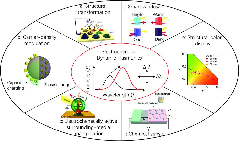
Fig. 1. Overview of electrochemistry enabled dynamic plasmonics: (a)–(c) approaches to realize dynamic plasmonics and (d)–(f) applications of dynamic plasmonics. (a) Reproduced with permission from Ref. 32, Copyright 2016, American Chemical Society. (b), (d) Reproduced with permission from Ref. 56, Copyright 2015, American Chemical Society. (c), (e) Reproduced with permission from Ref. 57, Copyright 2019, American Association for the Advancement of Science. (f) Reproduced with permission from Ref. 58, Copyright 2018, National Academy of Sciences.
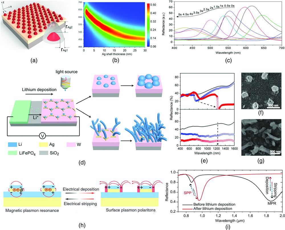
Fig. 2. Structural transformation for dynamic plasmonics. (a) Schematic of Au/Ag nanodome arrays. (b) Simulation of two-dimensional reflection spectra as a function of Ag shell thickness. (c) Measured reflection spectra of the device after different electrodeposition times. (d) Schematic of the morphology evolution during lithium deposition at different applied currents: lithium particle growth and disorder lithium dendrite formation. (e) Simulation reflectance of two lithium morphologies: shifts of reflectance dip and suppressed reflectance intensity. (f) The scanning electron microscope (SEM) image of lithium particles. (g) The SEM image of lithium dendrites. (h) Schematic of selective lithium deposition transferring metal–insulator–metal to the semi-infinite metallic grating. (i) The corresponding calculated reflection spectra switching between MPR and SPP. (a)–(c) Reproduced with permission from Ref. 32, Copyright 2016, American Chemical Society. (d)–(g) Reproduced with permission from Ref. 58, Copyright 2018, National Academy of Sciences. (h), (i) Reproduced with permission from Ref. 59, Copyright 2020, Wiley-VCH GmbH.
Fig. 3. Carrier-density modulation for dynamic plasmonics. (a) The SEM image of the colloidal silver particles. Inset is the transmission electron microscopy (TEM) image. (b) Absorption spectra of the silver solution at the open circuit potential of (a) In situ spectroelectrochemistry of 5% Nb-doped
Fig. 4. Electrochemically active surrounding-media manipulation for dynamic plasmonics. (a)–(d) Schematic, experimentally obtained reflectance spectra and FDTD simulated reflectance spectra of plasmochromic nanocavities based on a
Fig. 5. Applications of dynamic plasmonics: structural color displays. (a) Schematic of PANI-coated Au nanoparticles-based displays integrated with an electrochemical cell for scalable color generation. (b) Dark field images of Au nanoparticles with 20-, 40-, and 60-nm diameters during PANI redox reactions. (c) Color gamut (CIE 1931 chromaticity) of PANI-coated Au nanoparticles with 20-, 40-, and 60-nm diameters during PANI redox. (d) Device photo of PANI-coated Au nanoparticles before and after 3 months. Switching times of various plasmonic nanomaterials versus (e) the wavelength and (f) pixel areas. (a)–(f) Reproduced with permission from Ref. 57, Copyright 2019, American Association for the Advancement of Science.
Fig. 6. Applications of dynamic plasmonics: chemical sensors. (a)–(d) Electrocatalysis reaction sensors: (a) schematic of dark-field microscopy integrated with an electrochemical workstation for chemical reaction sensors; (b) schematic of the electrocatalytic oxidation reaction mechanism of In situ lithium dendrite detection with (i) applied current and (j) in situ reflectance. (a)–(d) Reproduced with permission from Ref. 110, Copyright 2014, American Chemical Society. (e)–(j) Reproduced with permission from Ref. 58, Copyright 2018, National Academy of Sciences.
|
Table 1. Summary of smart windows of various approaches.
|
Table 2. Summary of structural color displays of various approaches.

Set citation alerts for the article
Please enter your email address
© Copyright 2018-2021 | Chinese Laser Press. All Rights Reserved 沪ICP备15018463号-20