
Sumei Wang, Jinhua Zhao, Jinjun Gu, Mingyang Bu, Li Fan, Shuang Li, Xifeng Qin, Yicun Yao, Yingying Ren, Lei Wang. LiNbO3 channel and ridge waveguides based on helium ion implantation combined with lithography and precise diamond dicing[J]. Chinese Optics Letters, 2022, 20(7): 071301
- Chinese Optics Letters
- Vol. 20, Issue 7, 071301 (2022)
Abstract
1. Introduction
In recent decades, lithium niobate (, LN), with an oxygen octahedral structure, has been applied in photonic industry and considered to be optical “silicon”[
As an essential unit of integrated optical circuits, optical waveguides can limit and transmit light waves in the order of square microns by using the principle of total reflection at the interface of two materials with different refractive indices[
The main methods used to prepare optical waveguide structures in LN crystals are metal in-diffusion, proton exchange, ion implantation, femtosecond laser writing, and so on[
Sign up for Chinese Optics Letters TOC. Get the latest issue of Chinese Optics Letters delivered right to you!Sign up now
2. Experiment
To fabricate waveguides in LN crystals, -cut optical grade LN crystals with the size of were cleaned and implanted; the implantation energy was 500 keV, and the implantation fluence was at room temperature. During ion implantation, the samples were tilted 7° off the incident beam direction to prevent the channeling effect. The samples were annealed at 260°C in the air for 30 min after ion implantation to improve guiding quality.
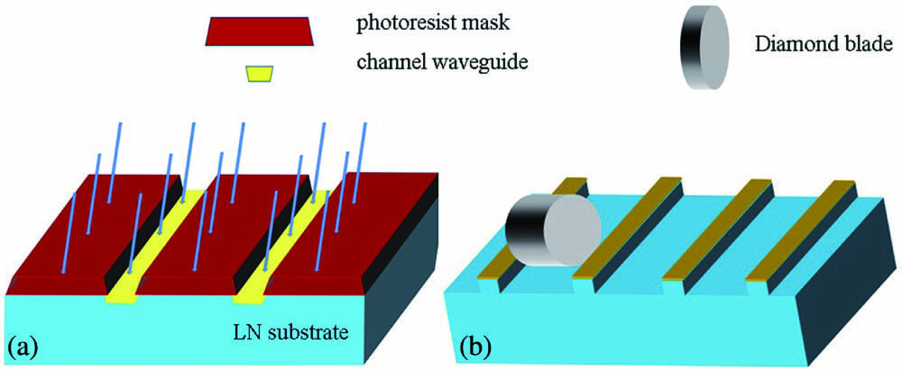
The schematics of the fabrication process for channel and ridge waveguides are illustrated in Figs. 1(a) and 1(b), respectively. As shown in Fig. 1(a), the channel waveguide was obtained by using standard lithography technology and the He ion implantation process. The thickness of the photoresist mask (BP-218) is sufficient to block high-energy ions, the openings () where ions can pass freely and be implanted into the LN substrate. After the standard lithography process, we obtained a photoresist mask of open strips 10 µm in width with a period of 50 µm. He ions were implanted into the unshielded region to obtain the channel waveguide (WG10). For comparison, the implantation (500 keV He ions, ) and subsequent annealing conditions (260°C for 30 min) of all samples were consistent.
![]()
Figure 1.Fabrication methods of LN waveguides: (a) channel guide; (b) ridge guide.
The preparation of the ridge waveguide consisted of two steps. The first step is obtaining the planar waveguide layer and then forming the ridges in specific areas by precise diamond dicing. The second step of the process is shown in Fig. 1(b). The cutting speed of the precision diamond blade is 40,000 r/min, and the moving speed is 0.5 mm/s. The width of the diamond blade used in the experiment was 50 µm. Two microgrooves were fabricated by using the diamond tool in one direction relative to the LN crystal, and a ridge waveguide was formed between the two microgrooves. Two kinds of the ridges were prepared with widths of 15 µm (WG15) and 25 µm (WG25) in the same LN crystal for direct comparison, but only the ridges with a width of 15 µm are shown in Fig. 1(b).
The displacement per atom (dpa) was calculated by using the calculation software for the stop and range of ions in matter (SRIM) 2013, and the refractive index profiles (RIPs) of the waveguides were reconstructed. Then, the dark-mode spectrum of the planar waveguide at the wavelength of 633 nm was measured by prism coupling equipment with a He–Ne laser at Shandong University. The prism coupler used in this paper is Model 2010 produced by Metricon Company in the United States. The end-face coupling technology is an intuitive and effective method for optical waveguides to study guiding properties and propagation losses. To better compare the optical properties of the channel and ridge waveguides, their propagation losses were measured by the end-face coupling method.
3. Results and Discussion
The dark-mode spectrum of the extraordinary refractive index () direction for the planar waveguide was measured by the prism coupling method after annealing at 260°C for 30 min with a wavelength of 633 nm. A sharp and deep dip is observed in the annealed LN planar waveguide, which corresponds to the true propagation mode [transverse magnetic () mode]. The effective refractive index () of the mode is larger than of the substrate (), which indicates an enhanced index well-formed in the near-surface region for the planar waveguide. There were some similar research results on the ion-implanted LN waveguide; for example, the values of the mode were 2.2109 (3 MeV O ion, )[
For integrated optical devices, the refractive index is one of the decisive factors in how propagating light is distributed in the waveguide structure. Given that this is a very critical parameter, we reconstructed the RIP based on the dpa profile and the prism coupling measurement results by adjusting the width of two half Gaussians[
![]()
Figure 2.(a) Dpa profile of 500 keV He ions with the fluence of 1.5 × 10¹⁶ ions/cm2 implanted into LN crystal by SRIM 2013; (b) reconstructed RIP of the LN waveguide after annealing at 260°C for 30 min at 633 nm.
![]()
Figure 3.(a) Profile of the TM0 guided mode simulated by BPM [one-dimensional (1D)]; (b) the modal intensity profile of TM0 mode computed by the BPM (2D); (c) near-field image of the TM0 mode by use of the end-face coupling method.
The metallographic microscope can be used to measure small changes in the refractive index. We observed the end faces of WG10, WG15, and WG25 with the Olympus BX51M microscope made in Japan, and all are shown in Figs. 4(a)–4(c), respectively. The bright areas have already been labeled to represent the guidance zones clearly. For WG10, the channel width is , and the channel interval is , whereas the ridge widths of the ridge waveguides are, respectively, available in two sizes, WG15 and WG25, and the ridge depth is , which is much larger than that of the waveguide layer. As can be seen from Figs. 4(b) and 4(c), it is inevitable to produce edge chipping during the precise diamond dicing process. The existence of the chipping has a certain influence on the quality of the ridge waveguides, and the influence decreases with the increase of ridge width.
![]()
Figure 4.Optical microscope image (×500) of the end face of waveguides after polishing: (a) WG10; (b) WG15; (c) WG25.
For investigating the optical properties of the 2D waveguides prepared, we used different measurement and simulation methods to obtain the RIPs, near-field profiles, and propagation losses. According to the size of the waveguide region obtained under the metallographic microscope in Fig. 4(a), a trapezoidal cross section of 9 µm for the upper base and 10 µm for the lower base was selected. Considering the trapezoidal cross section and the planar waveguide RIP shown in Fig. 2(b), the reconstructed RIP of WG10 is shown in Fig. 5(a). Using the same method, taking the RIP in Fig. 2(b) and the trapezoidal cross section in Fig. 4(b) into consideration, we calculated the RIP of WG15, and the result is displayed in Fig. 5(b). We only show the reconstructed RIP of WG15 here since the RIP of the ridge shapes of different widths is consistent in the vertical direction.
![]()
Figure 5.Reconstructed RIP of the waveguide: (a) WG10; (b) WG15.
The near-field intensity profiles of WG10 and WG15 were measured by the end-face coupling method. During the measurement, one microscope objective () focuses a beam with the wavelength of 633 nm into the waveguide to excite the guided mode, while the other microscope objective () collects light from the output end face of the sample, which is imaged onto the CCD camera. It can be seen from Figs. 6 and 7 that the optical waveguides can limit the light in both horizontal and vertical directions, indicating that we have successfully prepared 2D waveguides. The quasi-TM excitation modes (, , ) of WG10 and WG15 obtained by the end-face coupling method are shown in Figs. 6(a)–6(c) and 7(a)–7(c), while the simulation results computed by the BPM are shown in Figs. 6(d)–6(f) and 7(d)–7(f). The calculation results of WG10 and WG15 are in good agreement with the experimental results, indicating that the waveguides with a single mode in the Z direction and multi-mode in the X direction were formed. This also proves that the reconstructed RIPs can be consistent with the experiment results.
![]()
Figure 6.(a)–(c) Near-field image of WG10 quasi-TM modes from the end face of the sample captured by a CCD camera; (d)–(f) modal intensity profile computed by finite difference (FD)-BPM: quasi-TM00, TM10, TM20 modes. The color scale, which represents the relative light intensity, is shown also.
![]()
Figure 7.(a)–(c) Near-field image of WG15 quasi-TM modes from the end face of the sample captured by a CCD camera; (d)–(f) modal intensity profile computed by FD-BPM. The color scale, which represents the relative light intensity, is shown also.
The propagation loss is one of the vital parameters to evaluate the performance of the waveguide. We have used the experimental method to measure the propagation losses of WG10, WG15, and WG25, respectively[
| Waveguide | Coupling Efficiency | Propagation Loss (dB/cm) |
|---|---|---|
| WG10 | 50.16% | 3.42 |
| WG25 | 46.55% | 1.97 |
| WG15 | 46.72% | 12.4 |
Table 1. Coupling Efficiencies and Propagation Losses of the 2D Waveguides at 633 nm for TM Polarization
![]()
Figure 8.Experimental setup used with the end-face coupling method. Obj, microscope objective lens; location 1, the first position where the light power was measured; location 2, the second position where the light power was measured.
The propagation losses of the samples are shown in Table 1. As one can see, the propagation loss of WG10 is larger than that of WG25, and the difference in coupling efficiency may be one of the reasons for this result. However, the propagation loss of WG15 is greatly increased compared with that of other waveguides. The roughness of the sidewall that has a greater effect on WG15 may be the reason for this phenomenon. Next, we will further study the propagation losses of ridge waveguides with different widths and explore the factors that affect the propagation losses of ridge waveguides. Lithography and the precise diamond dicing technique have their advantages and disadvantages in preparing 2D waveguides. In general, the precise diamond dicing technique is simpler and more environmentally friendly than lithography for 2D waveguides. However, the application scope of precise diamond dicing technology is narrower, which is applied in ridge waveguides most of the time. Lithography can produce a wide variety of 2D waveguides, such as channel waveguides, curved waveguides, branching waveguides, and ridge waveguides. Through the study of this work, aiming at reducing propagation loss, lithography is more suitable for 2D waveguides with smaller widths (), whereas precise diamond dicing is a better choice to fabricate 2D waveguides with a larger width.
4. Conclusions
In conclusion, the channel waveguide was fabricated by He ion implantation in LN using a slotted photoresist mask to selectively implant the ions in certain areas of the substrate, and the ridge waveguides were prepared by He ion implantation combined with precise diamond dicing. The RIP simulation indicates that we have formed a “well” + “barrier” type optical waveguide. The channel waveguide and ridge waveguides were compared in terms of RIP, light intensity distribution, and propagation loss. For the wavelength of 633 nm, the propagation losses of WG10, WG25, and WG15 are 3.42 dB/cm, 1.97 dB/cm, and 12.4 dB/cm, respectively. As far as we know, the chipping created during the precise diamond dicing process is a factor that affects the propagation loss for ridge waveguides. From our work, we can conclude that lithography is more suitable with smaller widths (), whereas precise diamond dicing is a better choice for a larger width in the preparation of 2D optical waveguides combined with ion implantation technology. This work has a reference value for the application of LN waveguides in integrated photonic devices.
References
[1] R. Wolf, I. Breunig, H. Zappe, K. Buse. Scattering-loss reduction of ridge waveguides by sidewall polishing. Opt. Express, 26, 19815(2018).
[2] Y. Kong, F. Bo, W. Wang, D. Zheng, H. Liu, G. Zhang, R. Rupp, J. Xu. Recent progress in lithium niobate: optical damage, defect simulation, and on-chip devices. Adv. Mater., 32, 1806452(2020).
[3] S. Y. Siew, E. J. H. Cheung, H. Liang, A. Bettiol, N. Toyoda, B. Alshehri, E. Dogheche, A. J. Danner. Ultra-low loss ridge waveguides on lithium niobate via argon ion milling and gas clustered ion beam smoothening. Opt. Express, 26, 4421(2018).
[4] P. R. Sharapova, K. H. Luo, H. Herrmann, M. Reichelt, T. Meier, C. Silberhorn. Toolbox for the design of LiNbO3-based passive and active integrated quantum circuits. New J. Phys., 19, 123009(2017).
[5] I. Krasnokutska, J. J. Tambasco, X. Li, A. Peruzzo. Ultra-low loss photonic circuits in lithium niobate on insulator. Opt. Express, 26, 897(2018).
[6] Z. H. Chen, Y. W. Wang, H. H. Zhang, H. Hu. Silicon grating coupler on a lithium niobate thin film waveguide. Opt. Mater. Express, 8, 1253(2018).
[7] J. M. Lv, Y. Z. Cheng, J. R. V. de Aldana, X. T. Hao, F. Chen. Femtosecond laser writing of optical-lattice-like cladding structures for three-dimensional waveguide beam splitters in LiNbO3 crystal. J. Lightwave Technol., 34, 3587(2016).
[8] R. Schiek, A. S. Solntsev, D. N. Neshev. Temporal dynamics of all-optical switching in quadratic nonlinear directional couplers. Appl. Phys. Lett., 100, 111117(2012).
[9] M. R. Zhang, W. Ai, K. X. Chen, W. Jin, K. S. Chiang. A lithium-niobate waveguide directional coupler for switchable mode multiplexing. IEEE Photon. Technol. Lett., 30, 1764(2018).
[10] Y. Yao, W. Wang, B. Zhang. Designing MMI structured beam-splitter in LiNbO3 crystal based on a combination of ion implantation and femtosecond laser ablation. Opt. Express, 26, 19648(2018).
[11] J. Lv, Y. Cheng, J. R. Vazquez de Aldana, X. Hao, F. Chen. Femtosecond laser writing of optical-lattice-like cladding structures for three-dimensional waveguide beam splitters in LiNbO3 crystal. J. Lightwave. Technol., 34, 3587(2016).
[12] Q. Zhang, M. Li, J. Xu, Z. Lin, H. Yu, M. Wang, Z. Fang, Y. Cheng, Q. Gong, Y. Li. Reconfigurable directional coupler in lithium niobate crystal fabricated by three-dimensional femtosecond laser focal field engineering. Photonics Res., 7, 503(2019).
[13] P. Aashna, K. Thyagarajan. Polarization splitter based on a three waveguide directional coupler using quantum mechanical analogies. J. Opt., 19, 065805(2017).
[14] F. Chen, J. R. V. de Aldana. Optical waveguides in crystalline dielectric materials produced by femtosecond-laser micromachining. Laser Photon. Rev., 8, 251(2014).
[15] C. X. Liu, J. L. You, S. Q. Lin, J. Y. Chen, M. Tang, S. B. Lin, R. L. Zheng, L. L. Fu, L. L. Zhang. A ridge waveguide constructed by H+ implantation and precise diamond blade dicing in high-gain Nd3+-doped laser glass. Optik, 225, 165881(2021).
[16] A. Panepinto, D. Cossement, R. Snyders. Experimental and theoretical study of the synthesis of N-doped TiO2 by N ion implantation of TiO2 thin films. Appl. Surf. Sci., 541, 148493(2021).
[17] J. Rams, J. Olivares, P. J. Chandler, P. D. Townsend. Mode gaps in the refractive index properties of low-dose ion-implanted LiNbO3 waveguides. J. Appl. Phys., 87, 3199(2000).
[18] L. Wan, W. Luo, Y. Yuan, K. Zhang, S. Huang, S. Qiao, X. Pan, C. Wu. Effects of helium implantation fluence on the crystal-ion-slicing fabrication of Y-cut lithium niobate film. Mater. Express, 11, 717(2021).
[19] N. Cherkashin, N. Daghbouj, G. Seine, A. Claverie. Impact of He and H relative depth distributions on the result of sequential He+ and H+ ion implantation and annealing in silicon. J. Appl. Phys., 123, 161556(2018).
[20] S. M. Zhang, X. H. Liu, X. F. Qin, K. M. Wang, X. Liu. Damage, refractive index and near-field intensity profiles in a single-mode waveguide of LiNbO3 by 400 keV He ion implantation. J. Phys. D, 43, 455303(2010).
[21] J. Lin, F. Bo, Y. Cheng, J. Xu. Advances in on-chip photonic devices based on lithium niobate on insulator. Photonics Res., 8, 1910(2020).
[22] M. F. Volk, S. Suntsov, C. E. Ruter, D. Kip. Low loss ridge waveguides in lithium niobate thin films by optical grade diamond blade dicing. Opt. Express, 24, 1386(2016).
[23] J. H. Zhao, X. S. Jiao, Y. Y. Ren, J. J. Gu, S. M. Wang, M. Y. Bu, L. Wang. Lithium niobate planar and ridge waveguides fabricated by 3 MeV oxygen ion implantation and precise diamond dicing. Chin. Opt. Lett., 19, 060009(2021).
[24] Y. Cheng, J. Lv, S. Akhmadaliev, S. Zhou, Y. Kong, F. Chen. Mid-infrared ridge waveguide in MgO: LiNbO3 crystal produced by combination of swift O5+ ion irradiation and precise diamond blade dicing. Opt. Mater., 48, 209(2015).
[25] H. Hu, F. Lu, F. Chen, B. R. Shi, K. M. Wang, D. Y. Shen. Extraordinary refractive-index increase in lithium niobate caused by low-dose ion implantation. Appl. Opt., 40, 3759(2001).
[26] L. Wang, F. Chen, X. L. Wang, L. L. Wang, K.-M. Wang, L. Gao, H.-J. Ma, R. Nie. Si2+ ion implanted into stoichiometric lithium niobate crystals: waveguide characterization and lattice disorder analysis. Nucl. Instrum. Meth. B, 251, 104(2006).
[27] L. Wang, F. Chen, X.-L. Wang, K.-M. Wang, Y. Jiao, L.-L. Wang, X.-S. Li, Q.-M. Lu, H.-J. Ma, R. Nie. Low-loss planar and stripe waveguides in Nd3+-doped silicate glass produced by oxygen-ion implantation. J. Appl. Phys., 101, 053112(2007).

Set citation alerts for the article
Please enter your email address
© Copyright 2018-2021 | Chinese Laser Press. All Rights Reserved 沪ICP备15018463号-20