
Jiajing Yin, Yurun Sun, Shuzhen Yu, Yongming Zhao, Rongwei Li, Jianrong Dong. 1064 nm InGaAsP multi-junction laser power converters[J]. Journal of Semiconductors, 2020, 41(6): 062303
- Journal of Semiconductors
- Vol. 41, Issue 6, 062303 (2020)
Abstract
1. Introduction
Laser energy transmission as a potential technology of wireless energy transmission has attracted the attention of researchers in recent years. The laser power converter (LPC) is the core component of a laser energy transmission system and its conversion efficiency restricts the overall efficiency of the wireless energy transmission system. However, most of the research efforts on LPCs have focused on GaAs LPCs with a cut-off wavelength of 875 nm[
The open circuit voltage of a single-junction 1064 nm LPC is some 0.6–0.7 V, while several volts are usually required for power supplies in electronic systems. To make the LPCs practically useful for real situations, two schemes could be used to increase output voltage: the first is to connect multiple single-junction LPCs placed side-by-side in series[
The structures of InGaAsP triple-junction LPCs were grown by MOCVD, and LPCs with an aperture of 1 × 1 cm2 were fabricated. A conversion efficiency of 32.6% was achieved at a power density of 1.1 W/cm2 under 1064 nm laser irradiation at room temperature with an open-circuit voltage of 2.16 V and a fill factor of 0.74.
2. Theoretical and experimental details
2.1. Structure design and calculation of I–V characteristics of triple-junction InGaAsP LPC
The absorbing layer thicknesses of each sub-cell of the triple-junction InGaAsP LPCs are designed based on the rule of current matching and the absorption coefficient of InGaAsP material at 1064 nm. The thicknesses of the sub-cells can be determined using the following equation:
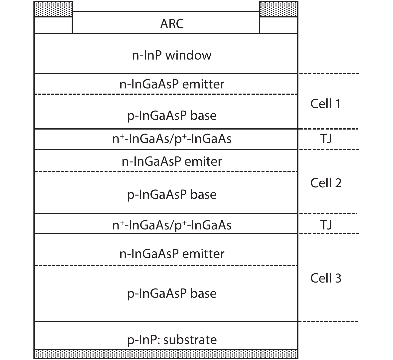
where α is the absorption coefficient, xn is the thickness of the absorbing layer of the nth sub-cell from the top, f is the percentage of the light being absorbed by the LPC, N is the number of the sub-cells. The ideal tunnel junction (TJ) connecting the sub-cells is transparent for the incident light. However, achieving both n-type and p-type doping concentration of more than 1 × 1019 cm–3 for InP and Al0.48In0.52As are difficult. Therefore, InGaAs is chosen to build the tunnel junctions for the triple-junction InGaAsP LPC. The depletion layer thickness of InGaAs TJ with a doping concentration of 1 × 1019 cm–3 on both sides is about 16 nm, and the thicknesses on two sides of the InGaAs pn junction are set to 20 nm considering the possible Zn diffusion. Fig. 1 shows the schematic structure of a vertically-stacked triple-junction InGaAsP LPC. Using 1.08 eV InGaAsP lattice matched to InP substrate as the absorption layer to obtain as high as possible voltage, while maintaining reasonable absorption coefficient at 1064 nm, the layer thicknesses of the triple-junction 1064 nm LPC are calculated to be 264, 456, and 2109 nm for cell 1, 2, and 3, respectively, based on the absorption coefficient of 1.4 × 104 cm–1 at 1064 nm for 1.08 eV InGaAsP[
![]()
Figure 1.Schematic layer structure of the designed triple-junction InGaAsP LPC.
The current–voltage (I–V) characteristic of the LPC was calculated and the loss mechanisms (e.g., series resistance, reflection of surface, and surface recombination) were taken into consideration during the calculation. The I–V characteristic of the multi-junction InGaAsP LPC can be described by the following equation:
where I is the output current, Iph the photogenerated current of sub-cell, Is the reverse saturation current, q the electron charge, V the output voltage, k the Boltzmann’s constant, T the temperature, n the ideality factor of the diode, N the number of sub-cells, Rs the series resistance, and Rsh the shunt resistance of the sub-cell.
Table 1 shows the parameters used for the calculation of the characteristics of the triple-junction InGaAsP LPCs with an aperture of 1 × 1 cm2.
Fig. 2 shows calculated I–V and P–V characteristics of the triple-junction InGaAsP LPC at an incident 1064 nm laser power density of 1 W/cm2 taking the absorption of the tunnel junctions into account, the short circuit current is 237.5 mA/cm2, the open circuit voltage is 2.174 V, the fill factor is 81.9%, and the conversion efficiency is 42.3%.
![]()
Figure 2.Calculated
2.2. Material growth and device processing
Prior to the growth of the triple-junction InGaAsP LPC structures, InGaAsP epitaxial layers were grown to calibrate the composition and growth rate. Room temperature photoluminescence (PL) peak at 1153 nm confirms the band gap of InGaAsP of 1.08 eV.
The triple-junction LPC epitaxial structure was grown on p-type InP substrates by an AIXTRON-200/4 MOCVD system using trimethylgallium (TMGa) and trimethylindium (TMIn), as well as arsine (AsH3) and phosphine (PH3) as the group III and group V precursors, respectively, and ultra-high purity hydrogen (H2) as the carrier gas. Diethylzinc (DEZn) and silane (SiH4) were used as the p-type and n-type doping sources, respectively. Starting from the InP substrate, a 300-nm InP buffer with a Zn concentration of 2 × 1018 cm−3 was grown followed by InGaAsP sub-cells of 2310, 456, and 264 nm thick, respectively, separated by 20-nm n+-InGaAs (Si: 2 × 1019 cm−3) /20-nm p+-InGaAs (Zn: 2 × 1019 cm−3) tunnel junctions, and finally a 500-nm InP current spreading layer and a 100-nm InGaAs contact layer with a Si concentration of 1 × 10¹⁸ and 2 × 1019 cm−3, respectively, were grown to finish the whole LPC structure. Each pn junction subcell comprised of a p-type and n-type layer doped with Zn and Si to 4 × 10¹⁷ and 2 × 1018 cm−3, respectively, and was sandwiched between a 50-nm InP back field layer doped with Zn of 2 × 1018 cm−3 and a 50-nm InP window layer doped with Si of 2 × 1018 cm−3.
Triple-junction InGaAsP LPC was fabricated by evaporating front grid and back ohmic contact metals, etching of InGaAs contact layer, and finally depositing 85-nm SiO2/100-nm TiO2 antireflection dielectric films. The reflectivity of the antireflection coating was measured using a reference sample and shown in Fig. 3, which confirmed the low reflection of 1.8% at 1064 nm. Subsequently, the LPC wafers were sawn into chips of 1 × 1 cm2. Silver paste was applied between LPC chips and Cu-plated ceramic heat sinks to improve thermal conductivity during the measurements.
![]()
Figure 3.Surface reflectance spectrum of the triple-junction InGaAsP LPCs with an antireflection coating.
3. Results and discussion
The measurement of laser LPC conversion efficiency was performed at room temperature, and the fiber guided 1064 nm optical beam with a divergence of about 25° perpendicularly illuminated the LPC chip surface with the end of the fiber at a distance to the surface to ensure that the whole light spot is received by the aperture. I–V curves of the triple-junction InGaAsP LPC under different 1064 nm monochromatic power densities of 610, 989, 1100, and 1233 mW/cm2 are shown in Fig. 4 and the extracted parameters are shown in Table 2.
![]()
Figure 4.
It can be seen from the Table 2 that the conversion efficiency of 32.13% at the optical power density of 989 mW/cm2 is much lower than the expected conversion efficiency of around 42.3% based on the design. A little bit higher conversion efficiency of 32.6% and higher open circuit voltage of 2.16 V are achieved at 1.1 W/cm2. The series resistance and shunt resistance are determined to be 0.22 and 43 Ω of the sub-cell, respectively, by fitting the I–V curve obtained at 1100 mW/cm2 using Eq. (2). The low shunt resistance indicates a significant leakage, probably via surface states of the side walls of the cell, which are not passivated by deposition of dielectrics.
To find the reasons why the conversion efficiency is lower than the expected efficiency, the external quantum efficiency (EQE) was measured using a xenon light source passing a monochromator and a standard Si cell as the reference. As shown in Fig. 5, the EQE at 1064 nm is 71.7% and is consistent with the short-circuit current of the triple-junction laser photovoltaic power converter. However, the EQE is much lower than the calculated EQE 84% assuming that the sub-cells are current-matched and the minority carrier lifetime is long enough for them to transport to the depletion layer and be separated by the built-in electric field, and finally collected by the electrodes to contribute to the output current.
![]()
Figure 5.External quantum efficiency of the triple-junction InGaAsP LPC.
There are two main causes that lower the conversion efficiency. The first is that the thicknesses of the sub-cells deviate from the optimal current-matching values due to inappropriate absorption coefficient is taken for the design of triple-junction InGaAsP cells, which leads to a current mismatch between sub-cells and output current is constrained by the lowest one and much smaller than the expected value. The second is that the internal quantum efficiency is lower than the assumed 95% resulting from a shorter carrier diffusion length. For the reference single junction InGaAsP cells with an absorbing layer thickness 3114 nm, the same as the total active layer thickness of the triple-junction InGaAsP cell, the EQE at 1064 nm is more than 80%. This means the diffusion length of the photogenerated minority carriers is larger than the thicknesses of the absorbing layers of the top and middle sub-cells, which are smaller than 0.5 μm. If the thicknesses of the sub-cells were designed to enable current-matching between the sub-cells, then the EQE of the triple-junction LPC should be larger than the single junction LPC because the thickness of the bottom cell is much smaller than that of the single junction LPC and carrier collection efficiency of the bottom cell is not less than that of the single junction LPC, which supports the current mismatch in our triple-junction LPC design. Therefore, while the minority carrier lifetime may not be long enough, it is not a bottleneck for the conversion efficiency of the triple-junction cells. Meanwhile, the low shunt resistance 132 Ω and high series resistance 0.66 Ω of the triple-junction LPC also contributes to the reduction of the efficiency.
The conversion efficiency of the LPC is 32.13% lower than the expected 42.3% at 1 W/cm2 by 10.17% (absolute value), of which 6.11% is due to the decrease of the short-circuit current, about 3.41% is attributed to the reduction of the fill factor, and the open-circuit voltage 2.14 V lower than the calculated 2.174 V caused an efficiency decrease of roughly 0.645%. Therefore, it is necessary to use the proper absorption coefficient to optimize the thicknesses of the absorbing layers of the sub-cells for current matching, to improve the quality of the material to increase the minority carrier lifetime, carrier diffusion length, and hence the internal quantum efficiency, and consequently to achieve a maximized short circuit current. In addition, because 20 nm p+-InGaAs/20 nm n+-InGaAs tunnel junction was used, the two tunnel junctions absorb about 4.7% of the incident light. The conversion efficiency of the InGaAsP LPC could be increased by some 2% (absolute value) by using non-absorbing p+-InP/n+-InP or p+-InGaAlAs/n+-InGaAlAs tunnel junction or the combination of the two.
4. Summary
We designed triple-junction InGaAsP photovoltaic devices to convert 1064 nm laser power into electric power with high output voltage, which are grown on InP substrates by MOCVD and processed into LPC chips. The performance of the LPCs are characterized at room temperature, and a conversion efficiency of 32.6% have been achieved for triple-junction InGaAsP LPCs of 1 × 1 cm2 under 1064 nm light illumination at a power density of 1.1 W/cm2 with a Voc of 2.16 V, Jsc of 225 mA/cm2 and an FF of 0.74. It is concluded that optimizing the thickness of absorbing layer and adopting non-absorption tunnel junction may significantly improve the conversion efficiency of InGaAsP triple-junction laser power converters.
Acknowledgments
This work was partially supported by the Jiangsu Province Science Foundation for Youths (No. BK20170431) and the National Natural Science Foundation of China (No. 61604171).
References
[1]
[2] E Oliva, F Dimroth, A W Bett. GaAs converters for high power densities of laserillumination. Prog Photovolt: Res Appl, 16, 289(2008).
[3] V Andreev, V Khvostikov, V Kalinovsky et al. High current density GaAs and GaSb photovoltaic cells for laser power beaming. IEEE World Conference on Photovoltaic Energy Conversion, 761(2003).
[4] S Fafard, F Proulx, M C A York et al. High-photovoltage GaAs vertical epitaxial monolithic heterostructures with 20 thin p/n junctions and a conversion efficiency of 60%. Appl Phys Lett, 109, 131107(2016).
[5]
[6] C E Valdivia, M M Wilkins, B Bouzazi et al. Five-volt vertically-stacked, single-cell GaAs photonic power converter. Physics, Simulation, Photonic Eng Photovolt Devices IV, 9358, 93580E(2015).
[7] S Safard, M C A York, F Proulx et al. Ultrahigh efficiencies in vertical epitaxial heterostructure architectures. Appl Phys Lett, 108, 071101(2016).
[8] M A Green, J Zhao, A Wang et al. 45 % efficient silicon photovoltaic cell under monochromatic light. IEEE Electron Device Lett, 13, 317(1992).
[9] V P Khvostikov, S V Sorokina, N S Potapovich et al. GaInAsP/InP-based laser power converters (λ = 1064 nm). Semiconductors, 52, 1748(2018).
[10] N Singh, C K F Ho, Y N Leong et al. InAlGaAs/InP-based laser photovoltaic converter at ~1070 nm. IEEE Electron Device Lett, 37, 1154(2016).
[11] S A Mintairov, V M Emelyanov, D V Rybalchenko et al. Heterostructures of metamorphic GaInAs photovoltaic converters fabricated by MOCVD on GaAs substrates. Semiconductors, 50, 517(2016).
[12] D V Rybalchenko, S A Mintairov, R A Salii et al. Metamorphic InGaAs photo-converters on GaAs substrates. J Phys: Conf Ser, 690, 012032(2016).
[13] D V Rybalchenko, S A Mintairov, R A Salii et al. Optimization of structural and growth parameters of metamorphic InGaAs photovoltaic converters grown by MOCVD. Semiconductors, 51, 93(2017).
[14] N A Kaluzhnyy, S A Mintaiov, A M Nadtochiy et al. InGaAs metamorphic laser (1064 nm) power converters with over 40% efficiency. Electron Lett, 53, 173(2017).
[15] Y Kim, H B Shin, W H Lee et al. 1080 nm InGaAs laser power converters grown by MOCVD using InAlGaAs metamorphic buffer layers. Sol Energy Mater Sol Cells, 200, 109984(2019).
[16] R Peña, C Algora. One-watt fiber-based power-by-light system for satellite applications. Prog Photovolt: Res Appl, 20, 117(2012).
[17] R Pena, C Algora. The influence of monolithic series connection on the efficiency of GaAs photovoltaic converters for monochromatic illumination. IEEE Trans Electron Devices, 48, 196(2001).
[18] C G Guan, W Liu, Q Gao. Influence of the mesa electrode position on monolithic on-chip series-interconnect GaAs laser power converter performance. Mater Sci Semicond Process, 75, 136(2018).
[19] J Schubert, E Oliva, F Dimroth. High-voltage GaAs photovoltaic laser power converters. IEEE Trans Electron Devices, 56, 170(2009).
[20] D Masson, F Proulx, S Fafard. Pushing the limits of concentrated photovoltaic solar cell tunnel junctions in novel high-efficiency GaAs phototransducers based on a vertical epitaxial heterostructure architecture. Prog Photovolts: Res Appl, 239, 1687(2015).
[21] M C A York, F Proulx, D P Masson et al. Thin n/p GaAs junctions for novel high-efficiency phototransducers based on a vertical epitaxial heterostructure architecture. MRS Adv, 1, 881(2016).
[22] S Fafard, F Proulx, M C A York et al. Advances with vertical epitaxial heterostructure architecture (VEHSA) phototransducers for optical to electrical power conversion efficiencies exceeding 50 percent. Physics Simulation Photonic Eng Photovolt Devices V, 9743, 974304(2016).
[23] F Proulx, M C A York, P O Provost et al. Measurement of strong photon recycling in ultra-thin GaAs n/p junctions monolithically integrated in high-photovoltage vertical epitaxial heterostructure architectures with conversion efficiencies exceeding 60%. Phys Status Solidi-Rapid Res Lett, 11, 1600385(2017).
[24] H Burkhard, H W Dinges, E Kuphal. Optical properties of In1–

Set citation alerts for the article
Please enter your email address
© Copyright 2018-2021 | Chinese Laser Press. All Rights Reserved 沪ICP备15018463号-20