
Qi'ao Dong, Wenqi Wang, Xinyi Cao, Yibo Xiao, Xiaohan Guo, Jingxuan Ma, Lianhui Wang, Li Gao. Plasmonic nanostructure characterized by deep-neural-network-assisted spectroscopy [Invited][J]. Chinese Optics Letters, 2023, 21(1): 010004
- Chinese Optics Letters
- Vol. 21, Issue 1, 010004 (2023)
Abstract
1. Introduction
Nanostructured metallic structures can induce the excitation of plasmonic resonance and confine the light field into the nanoscale regime. The choice of nanostructure geometry (such as shape, size, period, interparticle distance) and materials property (such as metal, thickness, dielectric coating) can alter the far-field resonant spectrum and near-field electromagnetic field, thus offering a giant optical tuning space for extraordinary photonic devices[1–3]. Such carefully designed plasmonic resonances have been applied in ultrasensitive biochemical detection[4,5], superresolution imaging[6–8], and structural colors[9–12], etc.
The exact light–matter interaction relies critically on the structure-response relationship; thus, a thorough understanding of the optical properties depends on an accurate nanostructure characterization[13–16]. The subwavelength nanostructure resonating in the visible wavelength regime has a lateral dimension on the order of 100 nm with different shapes, sizes, periods, and interparticle distances. The exact geometric parameters are usually characterized by advanced surface microscopic tools such as the scanning electron microscope (SEM) and atomic force microscope (AFM). However, the material properties such as metal film with tens of nanometers thickness are difficult to characterize and require delicate cross-sectional milling and examination. This is only accessible by expensive focused ion beam (FIB) milling and high-resolution SEM[15,16]. Moreover, different types of metals and transparent protective coatings on plasmonic nanostructures are also challenging to characterize without a priori information of its materials property, unless advanced material characterization tools can assist. Moreover, such accurate microscopic characterization is usually performed on specially prepared conductive and rigid substrates, where device damage is often unavoidable. It is also quite challenging to complete an easy and direct characterization on soft and nonconductive substrates.
As has been investigated extensively in recent years, deep-learning (DL)-based algorithms provide a revolutionary approach for inversely designing nanophotonic devices, as the physical relationship between the input and output layers can be accurately mapped through a multilayer perceptron[17–22]. By inputting desired nanophotonic resonance property such as amplitude, near-field or phase, the deep neural network (DNN) can output the nanophotonic structural design that can produce such optical responses. As the mapping between structure and spectrum is highly accurate and accessible by DNN, we propose to use such an architecture to achieve structural characterization by spectroscopic techniques. Very recently, Movsesyan et al. have successfully achieved accurate recognition of solution-processed plasmonic nanoparticles by using synthetic data trained by artificial neural networks[23]. Though the results are valid for theoretical conditions, there remains a question about whether DNN is applicable for experimentally obtained data, especially for recognizing large-area, periodic plasmonic nanostructures fabricated with processing variations.
Sign up for Chinese Optics Letters TOC. Get the latest issue of Chinese Optics Letters delivered right to you!Sign up now
In this work, we choose the large-area, quasi-3D plasmonic nanostructures that can be fabricated by low-cost and high-throughput nanoimprint lithography[15,16,24,25]. This technique allows us to generate hundreds of different experimental samples in a short period of time. The resulting plasmonic metasurface can be made into periodic nanoholes or nanopillars by depositing different metal films and dielectric coatings on soft substrates. The optical response is a collective effect of both geometric and material properties. While the lateral geometry can be quickly identified by an SEM, the parameters of metal type, metal film thickness, and dielectric coating of these plasmonic nanostructures are extremely difficult to characterize if no information is given beforehand or the samples are mixed up.
We first use simulated data of various plasmonic structures and their corresponding transmission spectra to train the DNN. After the training is completed, the input of an unknown spectrum can be characterized for its exact geometric parameters, such as structural type (nanohole or nanopillar), diameter and period, and its material parameters, such as metal type, thickness, and dielectric coating refractive index. Finally, by collecting a small number of experimental data, we demonstrate an accurate experimental characterization of the materials property after a DNN training of mixed experimental and simulated data. Our approach indicates DNN is robust to characterize accurate material parameters for unknown plasmonic nanostructures by just simple spectroscopic measurement.
2. Results
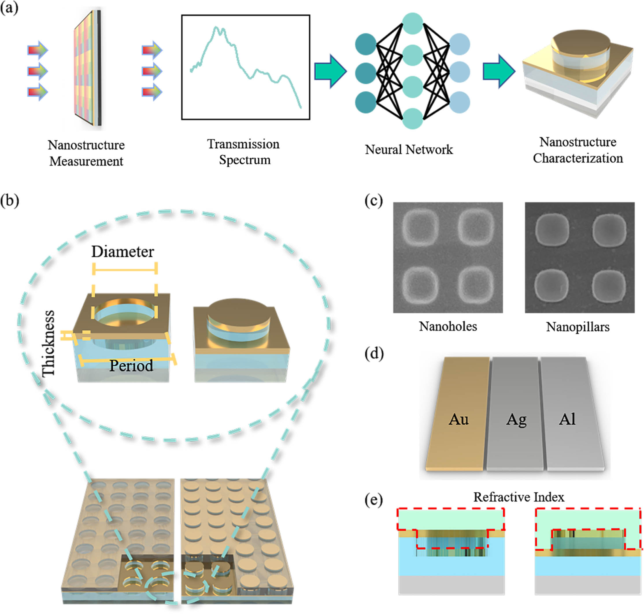
Figure 1(a) shows the methodology of using DNN to recognize the critical parameters of quasi-3D plasmonic nanostructures. We simulate or experimentally fabricate different plasmonic nanostructures with different characteristic parameters, such as the diameter, thickness, and period shown in Fig. 1(b), the structure type of nanohole and nanopillar shown in Fig. 1(c), different plasmonic metals, such as Au, Ag, and Al [Fig. 1(d)], and the refractive index of the protective dielectric coating shown in Fig. 1(e). Among these device parameters, we want to point out that although nanoholes and nanopillars can be easily differentiated side by side under a high resolution SEM, when only one type of structure is examined or dielectric coating is present over the surface, it is not straightforward to characterize its structural type. As shown in Fig. 1(a), the transmission spectra () are set up as input and the multiple plasmonic device parameters are set up as output. We collect the training data simulated by the finite-difference time-domain (FDTD, Lumerical, Inc.) method and construct four different DNNs.
![]()
Figure 1.Schematic diagram of the nanostructure characterization process and studied parameters. (a) Process flow of nanostructure characterization process; (b) periodic nanohole and nanopillar plasmonic nanostructure formed by nanoimprint lithography on glass substrate; (c) representative SEM images of the experimental samples of (b); (d) Au, Ag, and Al metal films evaporated on the structures; (e) dielectric coating covered on the structures to be identified for its refractive index.
We start with the simple case of an Au plasmonic device without dielectric coating. As illustrated in Fig. 2(a), we establish and train DNN1 using TensorFlow in Python, described in many works. The data set consists of 5250 groups of data simulated by FDTD, and the parameters are diameter ranging from 400 to 800 nm at a step size of 20 nm, period ranging from 1.4 to 1.7 times the diameters, and thickness of Au films ranging from 20 to 80 nm at a step size of 2.5 nm. The input dimension is as the transmission spectrum range is from 400 to 1400 nm with a 5 nm step size, and the output dimension is , corresponding to the structure type (nanohole or nanopillar), diameter, period, and the thickness of the Au film. The first hidden layer has 1000 nodes, while the other four layers have 670 nodes. Here we used the mean absolute error (MAE) instead of mean squared error (MSE) as the loss function[26]. Other settings include an Adamax optimizer and rectified linear unit (ReLU) activation function[27], as summarized in Table S1 (see Supplementary Material). The whole data set is divided into three parts randomly: 80% as the training data set, 10% as the validation data set, and the remaining 10% as the testing data set. After 1000 epochs of training, the DNN exhibits low loss (Fig. S1; see Supplementary Material) and high performance for both regression and classification problems. As shown in Figs. 2(b)–2(d), the absolute mean error of testing data set is 2.203 nm for diameter, 2.224 nm for period, and 0.417 nm for the thickness of the Au film. The relative mean error shown in Fig. 2(e) reaches 0.37% for diameter, 0.26% for period, and 0.86% for the thickness of the Au film. Among all 525 sets of testing data, 500, 474, and 517 sets exceed 98% accuracy for diameter, period, and thickness of Au film, as seen in Table 1. Here the accuracy is defined as
| Regression Problems | Classification Problems | |||||
|---|---|---|---|---|---|---|
| Parameters | Accuracy | Parameters | Truth | |||
| DNN1 Data size: 525 | Diameter | 525 | 517 | 500 | Structure type | 525 |
| Period | 525 | 523 | 474 | |||
| Thickness | 525 | 519 | 517 | |||
| DNN2 Data size: 735 | Diameter | 735 | 727 | 674 | Structure type | 735 |
| Period | 735 | 735 | 735 | Dielectric coating | 727 | |
| Thickness | 729 | 727 | 712 | |||
| DNN3 Data size: 3969 | Diameter | 3966 | 3857 | 3415 | Structure type | 3950 |
| Period | 3969 | 3951 | 3829 | Metal type | 3805 | |
| Thickness | 3621 | 3523 | 3413 | |||
| Refractive index | 3941 | 3933 | 3925 | |||
| DNN4 Data size: 4008 | Diameter | 3992 | 3842 | 3265 | Structure type | 3997 |
| Period | 3993 | 3957 | 3784 | Metal type | 3822 | |
| Thickness | 3596 | 3441 | 3261 | Data type | 4008 | |
| Refractive index | 3981 | 3947 | 3903 | |||
Table 1. Statistics of Characterization Error Distribution of DNNs
![]()
Figure 2.Results of DNN1. (a) The architecture of DNN1. The input layer has 201 neurons and the output layer has four neurons; there are five hidden layers. (b)–(d) The absolute error of the testing data set, where (b) is for diameter, (c) is for thickness, and (d) is for period. (e) Relative error of the testing data set; (f) example of two transmission spectra of the real structure and the predicted structure, with an MSE slightly higher than the mean value.
Furthermore, when it comes to the classification problems, the trained DNN can perfectly distinguish nanohole and nanopillar structures with an accuracy of 100%. In order to demonstrate the accuracy, we select a set of data with a slightly higher error than the mean value by simulating the spectrum of the DNN-predicted device parameters and comparing it with the original true spectrum [Fig. 2(f) and Table S2 (see Supplementary Material)]. We can see the two spectra are almost identical, with a mean squared error of .
Next, we simulate the more complex case where plasmonic device may be packaged by a protective dielectric coating. We add a layer of transparent dielectric materials on the Au plasmonic device, as shown in Fig. 1(e), including UV-curable optical adhesive NOA63, polymethyl methacrylate (PMMA), Microchem SU-8 photoresist, , and . The new data set consists of 7350 sets of simulated data. The DNN2 model is shown in Fig. S2(a) (see Supplementary Material) with five neurons in the output layer. As shown in Figs. S2(b)–S2(d) (see Supplementary Material), after 1000 epochs of training, the absolute error of the testing data set is 4.148 nm for diameter, 3.865 nm for period, and 0.273 nm for Au thickness. The relative errors shown in Fig. S2(e) (see Supplementary Material) are 0.72% for diameter, 0.43% for period, and 0.44% for the thickness of the Au film. As shown in Table 1, among 735 sets of testing data, there are 674, 735, and 712 sets exceeding 98% accuracy for diameter, period, and thickness of the Au film. The accuracy is slightly decreased for diameter and period. For classification problems, the accuracy is 100% for distinguishing between nanohole and nanopillar structures and 99.61% for identifying the five kinds of dielectric materials (only one set of data was identified incorrectly). We also plot a set of data so that the DNN has a slightly higher prediction error than the mean value and compare the spectra of the characterized structure and the real structure in Fig. S2(f) and Table S2 (see Supplementary Material), which shows a mean squared error of .
In a real application scenario, the refractive index of the dielectric coating or immersed solution is not specific, and the plasmonic materials are not limited to Au. Therefore, we consider multiple plasmonic metals of Au, Ag, and Al, and the refractive index of the coating or immersion layer varies from 1 to 3 with a step size of 0.25. The new data set consists of 39,690 sets of simulated data. As shown in Fig. 3(a), the output layer of DNN3 now has six parameters. After 600 epochs of training, the loss curves remain basically stable (Fig. S1; see Supplementary Material). As shown in Figs. 3(b)–3(e), the absolute error of the testing data set is 2.203 nm for diameter, 2.224 nm for period, 1.057 nm for thickness of the metal film, and 0.003 for the refractive index of the dielectric layer. The relative error shown in Fig. 3(f) reaches 0.97% for diameter, 0.56% for period, 0.18% for refractive index of the dielectric layer, and 2.46% for the metal thickness. Among 3960 sets of testing data, there are 3415, 3829, 3413, and 3925 sets showing accuracy over 98% for predicting diameter, period, thickness of metal film, and refractive index of dielectric layer (Table 1). The mean squared error of a typical characterized structure’s spectrum is , as shown in Fig. 3(g) and Table S2 (see Supplementary Material). For classification problems, the accuracy is 99.89% for distinguishing between nanohole and nanopillar structures and 96.8% for identifying Au, Ag, and Al. The characterization accuracy is slightly worse than the previous networks. The reason is attributed to the nonuniqueness problem encountered for increased output parameters and exponentially enlarged solution space[28]. We noticed that around 0.1% of the data groups’ output had very different device parameters with a highly similar spectrum (MSE less than ) to the true structure. This small fraction of nonunique mapping caused a decrease of average accuracy.
![]()
Figure 3.Results of DNN3. (a) The architecture of DNN3. The input layer has 201 neurons and the output layer has six neurons; there are five hidden layers. (b)–(e) The absolute error of the testing data set, where (b) is for diameter, (c) is for thickness, (d) is for period, and (e) is for the dielectric coating refractive index. (f) Relative error of the testing data set; (g) example of two transmission spectra of the real structure and the predicted structure, with an MSE slightly higher than the mean value.
For practical applications, we aim to characterize or identify a real plasmonic structure from its experimental spectrum. However, fabricating and collecting thousands of groups of experimental data for DNN training is a massive project, which can consume a long time and a big cost. Here in this work, we propose to collect a small portion of experimental spectra and mix them with simulated data for training and identifying the real nanostructures. We use soft nanoimprint lithography to fabricate 384 different plasmonic nanostructures with different metal, metal thickness, diameter, period, and dielectric coating, and measure their corresponding transmission spectra. Figures S3 and S4 (see Supplementary Material) show multiple sample images taken by an SEM; one typical nanohole and nanopillar structure is shown in Fig. 4(b). Figure 4(c) shows the experimental and simulated transmission spectra of the four samples, respectively. Most of the experimental and simulated transmission spectra for the same structural parameters resemble similar resonance features, while the spectral details are different, as the nanoimprinted samples show unavoidable defects and do not have a perfectly round shape, as those in simulations.
![]()
Figure 4.Results of DNN4. (a) The architecture of DNN4. The input layer has 201 neurons and the output layer has seven neurons; there are five hidden layers. (b) SEM images of nanohole and nanopillar structures prepared by nanoimprint lithography; (c) comparison of the experimental and simulated spectra; the yellow line indicates that the dielectric layer material is SU8, while the blue one indicates the air. (d) The absolute error of the testing data set; the top is the experimental data group, and the bottom is the total mixed data. (e) The relative error of the testing data set; the top is the experimental data, and the bottom is the total mixed data. (f) Statistics of the number of predictions that successfully identify the data type (experimental or simulated), structure type (nanohole or nanopillar), metal type, metal film thickness, and refractive index of dielectric layer collected for experimental data.
We mix this small set of experimental data (384 groups) with the large simulated data pool (39,690 groups) to form a mixed training data set (40,074 groups). We use a similar DNN4, shown in Fig. 4(a), with a new parameter of data type in the output layer to distinguish the experimental and simulated data type. After the training is done, we also use 10% of the data for testing. As shown in Figs. 4(d) and 4(e), the absolute error of the total testing data set is 7 nm for diameter, 6.46 nm for period, 1.3 nm for the thickness of the metal film, and 0.0028 for the refractive index of the dielectric layer. Specifically for experimental testing results, the error is 20.03 nm for diameter, 34.03 nm for period, 1.1 nm for the thickness of the metal film, and 0.004 for the refractive index of the dielectric layer. The relative error of the total testing data set is 1.25% for diameter, 0.72% for period, 3.05% for metal film thickness, and 0.27% for the refractive index of the dielectric layer, while the experimental part is 3.01% for diameter, 3.05% for period, 3.43% for the thickness of the metal film, and 2.58% for the refractive index of the dielectric layer. It is worth mentioning that the accuracy of classification problems reaches 100% for experimental data, which means the DNN can accurately identify the metal type and the structure type, as well as the data type. Here, we want to point out that DNN is not accurate enough to recognize the geometric parameters such as diameter and period of the experimental data. The reason is attributed to the error associated in SEM characterization with blurred edge and imperfect shape and size variation over the whole device [Fig. 4(b) and Figs. S3, S4 (see Supplementary Material)]. The approximate measurement error can range between 20 and 50 nm. If the experimental training data are not sufficiently accurate, it can lead to an incorrect mapping between input and output data.
With such experimental data limitation, we also attempted the transfer learning method described in relevant works[29]. By fixing the parameters of the hidden layers except the last one of the DNN trained by the simulation data, the transfer learning results of experimental data in the last layer are not satisfactory. However, the good accuracy of identifying structure type, metal type, metal thickness, and dielectric refractive index indicates the mixed data training model has great possibilities for application for characterizing material property that SEM or AFM tools are not capable of, or advanced material characterization tools can not easily access. Figure 4(f) shows the statistics of experimental characterization results of the data type (experimental or simulated), structure type (nanoholes or nanopillars), metal type, metal film thickness, and the refractive index of the dielectric layer, which all exhibit high accuracies. The criterion for judging whether the metal film thickness and refractive index of the dielectric layer are accurately identified is whether the predicted value is closest to the target one. Therefore, DNN can characterize the real device material property by mixed data training. In order to achieve accurate identification of both geometric and material parameters of a plasmonic nanostructure, we still need to seek a combination of DNN and conventional microscopic characterization, where materials property and geometric property can be identified separately. This method is worth exploration, as the nanostructure characterization of material composition and thickness is usually the most challenging. In this work, we only use a laptop whose CPU is i7-10750H and GPU is RTX 2070 for simulation and training DNNs. All the 39,690 sets of simulation data collection take about 800 hours. The 384 sets of experimental data collection take another two weeks’ time. When it comes to DNN training, even the most complex DNN just took tens of minutes. Once the one-time DNN training is finished, by just measuring the device transmission spectrum in a couple of minutes, nanostructure characterization for metal type, thickness, dielectric coating, and refractive index can be performed by DNN in just a few milliseconds. On the other hand, conventional advanced characterization for material composition, film thickness, and refractive index is very tedious, and it usually takes hours to days to complete one sample preparation and characterization, provided that those expensive tools are available.
3. Conclusion
In order to characterize multiple geometric and material properties of the plasmonic nanostructure, we have trained four DNNs with different complexity for different device application scenarios. As the characterizing parameter increases, the general recognition accuracy of diameter and period decreases. We have also reported the network training by a mixture of experimental and simulated data, and the resulting DNN can yield an accurate material characterization. The metal type and thickness, structure, data type, dielectric coating, and refractive index can all be identified accurately. Our results indicate the ease of experimental data acquisition burden for DNN training, and the potential of computational structural characterization.
4. Methods
4.1. Device fabrication
The pattern is replicated using UV-assisted nanoimprinting (UV-NI) to imprint the PDMS stamp nanostructures onto a glass substrate coated with UV-curable resist (NOA 63). While maintaining the pressure, the resist is cured under UV irradiation, producing nanostructures with imprint depth. Then a thin layer of metal (Au, Ag) is deposited on the replicated pattern using electron beam evaporation. Lastly, a layer of dielectric coating such as SU8 photoresist is spin-coated as protective dielectric coating at a speed of 3000 r/min.
4.2. Training process of DNNs
Our networks are built using Keras. The training process uses Adamax as the optimizer, MAE as the loss function, and the ReLU as the activation. MAE is defined as
4.3. Simulations
Simulations of the transmission spectra were performed by using a simulation tool based on the FDTD method. Simulations were performed with a plane wave under normal incidence.
4.4. Optical characterization
The SEM images of the fabricated samples were taken under a high-resolution SEM (S-4800, Hitachi). The optical transmission spectra were measured under the normal incidence using a PE UV-Vis spectrophotometer (LAMBDA 650S).
References
[1] M. B. Ross, C. A. Mirkin, G. C. Schatz. Optical properties of one-, two-, and three-dimensional arrays of plasmonic nanostructures. J. Phys. Chem. C, 120, 816(2016).
[2] M. Mayer, M. J. Schnepf, T. A. König, A. Fery. Colloidal self-assembly concepts for plasmonic metasurfaces. Adv. Opt. Mater., 7, 1800564(2019).
[3] C. Valsecchi, A. G. Brolo. Periodic metallic nanostructures as plasmonic chemical sensors. Langmuir, 29, 5638(2013).
[4] B. Špačková, P. Wrobel, M. Bocková, J. Homola. Optical biosensors based on plasmonic nanostructures: a review. Proc. IEEE, 104, 2380(2016).
[5] Y. Zhang, Z. Shuai, H. Zhou, Z. Luo, B. Liu, Y. Zhang, L. Zhang, S. Chen, J. Chao, L. Weng. Single-molecule analysis of microRNA and logic operations using a smart plasmonic nanobiosensor. J. Am. Chem. Soc., 140, 3988(2018).
[6] D. Lu, Z. Liu. Hyperlenses and metalenses for far-field super-resolution imaging. Nat. Commun., 3, 1205(2012).
[7] A. Bezryadina, J. Zhao, Y. Xia, X. Zhang, Z. Liu. High spatiotemporal resolution imaging with localized plasmonic structured illumination microscopy. ACS Nano, 12, 8248(2018).
[8] D. L. Mack, E. Cortés, V. Giannini, P. Török, T. Roschuk, S. A. Maier. Decoupling absorption and emission processes in super-resolution localization of emitters in a plasmonic hotspot. Nat. Commun., 8, 1(2017).
[9] S. J. Tan, L. Zhang, D. Zhu, X. M. Goh, Y. M. Wang, K. Kumar, C.-W. Qiu, J. K. Yang. Plasmonic color palettes for photorealistic printing with aluminum nanostructures. Nano Lett., 14, 4023(2014).
[10] K. Kumar, H. Duan, R. S. Hegde, S. C. Koh, J. N. Wei, J. K. Yang. Printing colour at the optical diffraction limit. Nat. Nanotechnol., 7, 557(2012).
[11] X. Duan, S. Kamin, N. Liu. Dynamic plasmonic colour display. Nat. Commun., 8, 14606(2017).
[12] S. D. Rezaei, R. J. Hong Ng, Z. Dong, J. Ho, E. H. Koay, S. Ramakrishna, J. K. Yang. Wide-gamut plasmonic color palettes with constant subwavelength resolution. ACS Nano, 13, 3580(2019).
[13] P. R. Wiecha, A. Lecestre, N. Mallet, G. Larrieu. Pushing the limits of optical information storage using deep learning. Nat. Nanotechnol., 14, 237(2019).
[14] L. Gao, Y. Zhang, H. Zhang, S. Doshay, X. Xie, H. Luo, D. Shah, Y. Shi, S. Xu, H. Fang. Optics and nonlinear buckling mechanics in large-area, highly stretchable arrays of plasmonic nanostructures. ACS Nano, 9, 5968(2015).
[15] L. Gao, K. Shigeta, A. Vazquez-Guardado, C. J. Progler, G. R. Bogart, J. A. Rogers, D. Chanda. Nanoimprinting techniques for large-area three-dimensional negative index metamaterials with operation in the visible and telecom bands. ACS Nano, 8, 5535(2014).
[16] L. Gao, Y. Kim, A. Vazquez-Guardado, K. Shigeta, S. Hartanto, D. Franklin, C. J. Progler, G. R. Bogart, J. A. Rogers, D. Chanda. Materials selections and growth conditions for large-area, multilayered, visible negative index metamaterials formed by nanotransfer printing. Adv. Opt. Mater., 2, 256(2014).
[17] G. Yoon, K. Kim, S.-U. Kim, S. Han, H. Lee, J. Rho. Printable nanocomposite metalens for high-contrast near-infrared imaging. ACS Nano, 15, 698(2021).
[18] W. Ma, Z. Liu, Z. A. Kudyshev, A. Boltasseva, W. Cai, Y. Liu. Deep learning for the design of photonic structures. Nat. Photon., 15, 77(2021).
[19] S. So, J. Rho. Designing nanophotonic structures using conditional deep convolutional generative adversarial networks. Nanophotonics, 8, 1255(2019).
[20] S. So, T. Badloe, J. Noh, J. Bravo-Abad, J. Rho. Deep learning enabled inverse design in nanophotonics. Nanophotonics, 9, 1041(2020).
[21] T. Zhang, J. Wang, Q. Liu, J. Zhou, J. Dai, X. Han, Y. Zhou, K. Xu. Efficient spectrum prediction and inverse design for plasmonic waveguide systems based on artificial neural networks. Photonics Res., 7, 368(2019).
[22] D. Liu, Y. Tan, E. Khoram, Z. Yu. Training deep neural networks for the inverse design of nanophotonic structures. ACS Photonics, 5, 1365(2018).
[23] S. Molesky, Z. Lin, A. Y. Piggott, W. Jin, J. Vucković, A. W. Rodriguez. Inverse design in nanophotonics. Nat. Photon., 12, 659(2018).
[24] A. Movsesyan, L. V. Besteiro, Z. Wang, A. O. Govorov. Mie sensing with neural networks: recognition of nano-object parameters, the invisibility point, and restricted models. Adv. Theor. Simul., 5, 2100369(2022).
[25] X. Cao, Y. Xiao, Q. Dong, S. Zhang, J. Wang, L. Wang, L. Gao. Tuning metasurface dimensions by soft nanoimprint lithography and reactive ion etching. Adv. Photon. Res., 2200127(2022).
[26] Q. Wu, X. Li, W. Wang, Q. Dong, Y. Xiao, X. Cao, L. Wang, L. Gao. Comparison of different neural network architectures for plasmonic inverse design. ACS Omega, 6, 23076(2021).
[27] D. P. Kingma, J. Ba. Adam: a method for stochastic optimization(2014).
[28] S. So, J. Mun, J. Rho. Simultaneous inverse design of materials and structures via deep learning: demonstration of dipole resonance engineering using core–shell nanoparticles. ACS Appl. Mater. Interfaces, 11, 24264(2019).
[29] C. Lee, J. Na, K. Park, H. Yu, J. Kim, K. Choi, D. Park, S. Park, J. Rho, S. Lee. Development of artificial neural network system to recommend process conditions of injection molding for various geometries. Adv. Intell. Syst., 2, 2000037(2020).

Set citation alerts for the article
Please enter your email address
© Copyright 2018-2021 | Chinese Laser Press. All Rights Reserved 沪ICP备15018463号-20