
Chong Zhang, Jingpei Hu, Yangeng Dong, Aijun Zeng, Huijie Huang, Chinhua Wang. High efficiency all-dielectric pixelated metasurface for near-infrared full-Stokes polarization detection[J]. Photonics Research, 2021, 9(4): 583
- Photonics Research
- Vol. 9, Issue 4, 583 (2021)
Abstract
1. INTRODUCTION
Polarization, the same as intensity, wavelength, and phase, is an important characteristic of light. Conventional imaging techniques only capture the intensity and spectral information of light, but ignore the polarization information in the scene. Deeper information about the materials, like surface shape, roughness, optical activity of the materials, and chemical properties, can be obtained from the polarization state of light. Polarimetric imaging techniques can obtain polarization state of light over a scene of interest, which play an important role in many applications, such as astronomy [1], chemical analysis [2], remote sensing [3–5], and biomedical diagnosis [6,7].
Conventional polarimetry approaches rely on mechanically rotating polarizers [8] and retardation wave plates [9] several times, which takes long acquisition time and is unavailable for dynamic events. Moreover, the optical components are bulky and do not conform to the current trends of integration and miniaturization [10,11]. Pixelated metasurfaces [12–14] combined with a charge coupled device (CCD) to obtain real-time polarization imaging can overcome the shortcomings of the conventionally mechanical rotating polarization imaging, which can acquire the polarization state of incident light at one time. These methods are more compact and less expensive, require less convoluted optic systems, and are the primary development directions of polarization imaging in the future. As we all know, the polarization state of light is usually described by Stokes vector , comprised by four components (, , , ), which are related to the intensities of linearly and circularly polarized parts of the incident light. Most of the pixelated metasurfaces are composed of nanowire-grid polarization filters [15–17] in different directions, which work on linearly polarized light but not circularly polarized light, so only part of the Stokes vector (, , ) can be detected through it.
Over the past years, metasurfaces with great design flexibility and ultracompact form factors provide a great choice for circularly polarized light detection and have attracted lots of attention [18–25]. Among these designs, three-dimensional (3D) chiral plasmonic metasurfaces can acquire a higher circular polarization (CP) extinction ratio than the planar chiral plasmonic metasurfaces. However, these 3D metasurfaces are difficult to integrate with nanowire-grid polarization filters on a single layer. To overcome this difficulty, double-layer planar plasmonic metasurfaces consisting of waveplates and polarizers as CP filters were designed and fabricated, while the transmission of the filters is extremely low [26,27], and their fabrication technology is complex [26–28]. Compared with plasmonic metasurfaces, all-dielectric structures avoid absorption losses and have compatibility with available semiconductor industry technologies. Recently, all-dielectric metasurfaces composed of multiple microscale scatterers, which split and focus light in four or six different polarization bases, were reported with high transmission to realize full-Stokes detection of incident light [11,29–31]. However, these kinds of metasurfaces can only be designed for a single wavelength, and the crosstalk between different polarization states interferes with the measurement results when the super-pixel becomes smaller.
Sign up for Photonics Research TOC. Get the latest issue of Photonics Research delivered right to you!Sign up now
Here, we propose and experimentally demonstrate ultracompact high performance all-dielectric pixelated full-Stokes metasurfaces for the near-infrared wavelength. Each pixel consists of linear polarizers in three directions and one circular polarizer with single-layer planar structures. All of these polarizers can be integrated on a silicon-on-insulator (SOI) chip, which is compatible with mature semiconductor industry technologies nowadays. The proposed all-dielectric pixelated full-Stokes metasurfaces are more advantageous due to their ultracompactness, high extinction ratio, high transmission efficiencies, and broad operating wavelength, which can meet the measurement requirements of many applications.
2. PIXELATED METASURFACE DESIGN
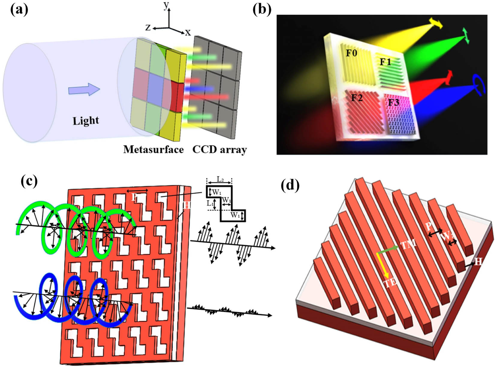
Figure 1.Schematic of setup for near-infrared full-Stokes detection. (a) Polarization measurement device with the metasurface and the CCD array. Each pixel of the metasurface is composed of four different polarization filters. (b) Three-dimensional schematic of the pixel unit with four spatially distributed polarization filters. The colors are used only for distinguishment of the image and bear no wavelength information. (
As we know, the full-Stokes vectors have four parameters , , , and are defined as
![]()
Figure 2.Simulation performances of the CP filters. (a) Transmission spectra of the CP filter for RCP (black) and LCP (red) light as the parameters of the Z-shaped pattern are as follows:
![]()
Figure 3.Simulation performances of the LP filters. (a) Transmission spectra of the LP filter for TM (black) and TE (red) light as the parameters of nanowire gratings are as follows:
3. FABRICATION AND EXPERIMENTAL RESULTS
![]()
Figure 4.Scanning electron microscope (SEM) image. (a) SEM image of the fabricated devices. (b) Enlarged SEM image of the LP filters with nanowire gratings. (c) Enlarged SEM image of the CP filters with the Z-shaped pattern.
![]()
Figure 5.Experimental setup and measurement results of the LP and CP filters. (a) Schematic of the measurement setup for CP filter characterization. (b) Transmission spectra of RCP and LCP light and (c) corresponding CD of the CP filter. (d) Transmission spectra of TM and TE polarized light and (e) corresponding extinction ratio of the LP filter.
After removing the QWP and replacing the CP filter with the LP filter, the performance of the LP filter can be directly tested. The measured transmission spectra for TE and TM polarized light of the LP filter are shown in Fig. 5(d). The average transmission for TM polarized light is measured at around 75% in the wavelength range of 1.47 μm to 1.6 μm. The corresponding extinction ratio is shown in Fig. 5(e). It is indicated that the extinction ratio is greater than 20 dB in the wavelength range from 1.49 μm to 1.6 μm, and the maximum can reach 34 dB at 1.52 μm. Compared with the theoretical results, the peak of the corresponding extinction ratio shows a slight blue shift and declines significantly. The slight blue shift may be caused by over etching in the fabrication, and the reason for the decline of the extinction ratio is associated with the sensitivity of the photodetector. When the transmission of TE polarized light is lower than the lowest sensitivity of the detector, the optical signal can be drowned by noise, which significantly reduces the maximum extinction ratio. From these experiment results of the LP and CP filters, the metasurface is competent to detect the full-Stokes vector of incident light in the wavelength ranges from 1.49 μm to 1.54 μm and from 1.59 μm to 1.61 μm.
4. CONCLUSION
In conclusion, we designed and fabricated a pixelated all-dielectric metasurface based on the SOI substrate for full-Stokes vector detection in the near-infrared band. The pixel unit of the metasurface is composed of four different polarization filters including LP and CP filters. With equal etching depths, periods, and simple structure, the CP and LP filters are easily integrated on the same chip, which is compatible with conventional semiconductor industry technologies. We experimentally demonstrated the performance of the metasurface by testing the polarization effects of different filters, respectively. With a simple two-dimensional etching pattern, the CP filters can well distinguish the handedness of circularly polarized light with CD as high as 70% at 1.6 μm and average transmission efficiency of more than 80% from 1.48 μm to 1.6 μm. By optimizing the parameters of the grating in the same operation wavelength band, the LP filters have a great polarization effect for linearly polarized light. Comparably, our device has great potential for near-infrared polarimeters and on-chip polarimetric imaging systems, which are desirable for material characterization, medical diagnosis, biomedical imaging, and molecular spectroscopy.
References
[1] J. B. Breckinridge, B. R. Oppenheimer. Polarization effects in reflecting coronagraphs for white-light applications in astronomy. Astrophys. J., 600, 1091-1098(2004).
[2] L. A. Nafie, T. B. Freedman. Vibrational circular dichroism: an incisive tool for stereochemical applications. Enantiomer, 3, 283-297(1998).
[3] N. J. Pust, J. A. Shaw. Digital all-sky polarization imaging of partly cloudy skies. Appl. Opt., 47, H190-H198(2008).
[4] J. S. Tyo, D. H. Goldstein, D. B. Chenault, J. A. Shaw. Polarization in remote sensing-introduction. Appl. Opt., 45, 5451-5452(2006).
[5] J. S. Tyo, D. L. Goldstein, D. B. Chenault, J. A. Shaw. Review of passive imaging polarimetry for remote sensing applications. Appl. Opt., 45, 5453-5469(2006).
[6] M. Dubreuil, P. Babilotte, L. Martin, D. Sevrain, S. Rivet, Y. L. Grand, G. L. Brun, B. Turlin, B. L. Jeune. Mueller matrix polarimetry for improved liver fibrosis diagnosis. Opt. Lett., 37, 1061-1063(2012).
[7] R. Patel, A. Khan, R. Quinlan, A. N. Yaroslavsky. Polarization sensitive multimodal imaging for detecting breast cancer. Cancer Res., 74, 4685-4693(2014).
[8] H. G. Berry, G. Gabrielse, A. E. Livingston. Measurement of the Stokes parameters of light. Appl. Opt., 16, 3200-3205(1977).
[9] R. M. A. Azzam, N. M. Bashara. Ellipsometry and Polarized Light(1977).
[10] K. P. Gurton, A. J. Yuffa, G. W. Videen. Enhanced facial recognition for thermal imagery using polarimetric imaging. Opt. Lett., 39, 3857-3859(2014).
[11] S. Wei, Z. Yang, M. Zhao. Design of ultracompact polarimeters based on dielectric metasurfaces. Opt. Lett., 42, 1580-1583(2017).
[12] Z. Zhang, F. Dong, K. Qian, Q. Zhang, W. Chu, Y. Zhang, X. Ma, X. Wu. Real-time phase measurement of optical vortices based on pixelated micropolarizer array. Opt. Express, 23, 20521-20528(2015).
[13] X. Ma, F. Dong, Z. Zhang, Y. Su, T. Xu, Z. Jiang, S. Wu, Q. Zhang, W. Chu, X. Wu. Pixelated-polarization-camera-based polarimetry system for wide real-time optical rotation measurement. Sens. Actuators B, 283, 857-864(2019).
[14] J. Guo, D. Brady. Fabrication of thin-film micropolarizer arrays for visible imaging polarimetry. Appl. Opt., 39, 1486-1492(2000).
[15] V. Gruev, A. Ortu, N. Lazarus, J. Van der Spiegel, N. Engheta. Fabrication of a dual-tier thin film micropolarization array. Opt. Express, 15, 4994-5007(2007).
[16] V. Gruev, R. Perkins, T. York. CCD polarization imaging sensor with aluminum nanowire optical filters. Opt. Express, 18, 19087-19094(2010).
[17] G. P. Nordin, J. T. Meier, P. C. Deguzman, M. W. Jones. Micropolarizer array for infrared imaging polarimetry. J. Opt. Soc. Am. A, 16, 1168-1174(1999).
[18] Z. Yang, M. Zhao, P. Lu, Y. Lu. Ultrabroadband optical circular polarizers consisting of double-helical nanowire structures. Opt. Lett., 35, 2588-2590(2010).
[19] B. Frank, X. Yin, M. Schäferling, J. Zhao, S. M. Hein, P. V. Braun, H. Giessen. Large-area 3D chiral plasmonic structures. ACS Nano, 7, 6321-6329(2013).
[20] M. Zhang, V. Pacheco-Peña, Y. Yu, W. Chen, N. J. Greybush, A. Stein, N. Engheta, C. B. Murray, C. R. Kagan. Nanoimprinted chiral plasmonic substrates with three-dimensional nanostructures. Nano Lett., 18, 7389-7394(2018).
[21] J. K. Gansel, M. Thiel, M. S. Rill, M. Decker, K. Bade, V. Saile, G. Freymann, S. Linden, M. Wegener. Gold helix photonic metamaterial as broadband circular polarizer. Science, 325, 1513-1515(2009).
[22] M. Decker, M. Klein, M. Wegener, S. Linden. Circular dichroism of planar chiral magnetic metamaterials. Opt. Lett., 32, 856-858(2007).
[23] D. Kwon, P. L. Werner, D. H. Werner. Optical planar chiral metamaterial designs for strong circular dichroism and polarization rotation. Opt. Express, 16, 11802-11807(2008).
[24] F. Afshinmanesh, J. S. White, W. Cai, M. L. Brongersma. Measurement of the polarization state of light using an integrated plasmonic polarimeter. Nanophotonics, 1, 125-129(2012).
[25] W. Ye, X. Yuan, C. Guo, J. Zhang, B. Yang, S. Zhang. Large chiroptical effects in planar chiral metamaterials. Phys. Rev. Appl., 7, 054003(2017).
[26] J. Dong, J. Zhou, T. Koschny, C. Soukoulis. Bi-layer cross chiral structure with strong optical activity and negative refractive index. Opt. Express, 17, 14172-14179(2009).
[27] J. Bai, C. Wang, X. Chen, A. Basiri, C. Wang, Y. Yao. Chip-integrated plasmonic flat optics for mid-infrared full-Stokes polarization detection. Photon. Res., 7, 1051-1060(2019).
[28] A. Basiri, X. Chen, J. Bai, P. Amrollahi, J. Carpenter, Z. Holman, C. Wang, Y. Yao. Nature-inspired chiral metasurfaces for circular polarization detection and full-Stokes polarimetric measurements. Light Sci. Appl., 8, 78(2019).
[29] A. Arbabi, Y. Horie, M. Bagheri, A. Faraon. Dielectric metasurfaces for complete control of phase and polarization with subwavelength spatial resolution and high transmission. Nat. Nanotechnol., 10, 937-943(2015).
[30] E. Arbabi, S. M. Kamali, A. Arbabi, A. Faraon. Full-Stokes imaging polarimetry using dielectric metasurfaces. ACS Photon., 5, 3132-3140(2018).
[31] C. Yan, X. Li, M. Pu, X. Ma, F. Zhang, P. Gao, K. Liu, X. Luo. Midinfrared real-time polarization imaging with all-dielectric metasurfaces. Appl. Phys. Lett., 114, 161904(2019).
[32] J. Hu, X. Zhao, Y. Lin, A. Zhu, X. Zhu, P. Guo, B. Cao, C. Wang. All-dielectric metasurface circular dichroism waveplate. Sci. Rep., 7, 41893(2017).
[33] M. M. Rahman, A. Khaleque, M. T. Rahman, F. Rabbi. Gold-coated photonic crystal fiber based polarization filter for dual communication windows. Opt. Commun., 461, 125293(2020).
[34] M. V. Gorkunov, V. E. Dmitrienko, A. A. Ezhov, V. V. Artemov, O. Y. Rogovet. Implications of the causality principle for ultra chiral metamaterials. Sci. Rep., 5, 9273(2015).
[35] E. D. Palik. Handbook of Optical Constants of Solids(1997).
[36] S. Chou, W. Deng. Subwavelength amorphous silicon transmission gratings and applications in polarizers and waveplates. Appl. Phys. Lett., 67, 742-744(1995).
[37] Z. Zhang, F. Dong, T. Cheng, K. Qiu, Q. Zhang, W. Chu, X. Wu. Nano-fabricated pixelated micropolarizer array for visible imaging polarimetry. Rev. Sci. Instrum., 85, 105002(2014).

Set citation alerts for the article
Please enter your email address
© Copyright 2018-2021 | Chinese Laser Press. All Rights Reserved 沪ICP备15018463号-20