• Photonics Research
  • Vol. 10, Issue 2, A14 (2022)
Gaehun Jo1, Pierre Edinger1, Simon J. Bleiker1, Xiaojing Wang1, Alain Yuji Takabayashi2, Hamed Sattari2, Niels Quack2, Moises Jezzini3, Jun Su Lee3, Peter Verheyen4, Iman Zand5, Umar Khan5, Wim Bogaerts5, Göran Stemme1, Kristinn B. Gylfason1、6、*, and Frank Niklaus1、7、*
Author Affiliations
  • 1Division of Micro and Nanosystems, KTH Royal Institute of Technology, 11428 Stockholm, Sweden
  • 2École Polytechnique Fédérale de Lausanne (EPFL), 1015 Lausanne, Switzerland
  • 3Tyndall National Institute, Lee Maltings Complex Dyke Parade, T12 R5CP Cork, Ireland
  • 4imec vzw. 3DSIP Department, Si Photonics Group, Kapeldreef 75, 3001 Leuven, Belgium
  • 5Department of Information Technology, Photonics Research Group, Ghent University - IMEC, 9052 Gent, Belgium
  • 6e-mail: gylfason@kth.se
  • 7e-mail: frank@kth.se
  • show less
    DOI: 10.1364/PRJ.441215 Cite this Article Set citation alerts
    Gaehun Jo, Pierre Edinger, Simon J. Bleiker, Xiaojing Wang, Alain Yuji Takabayashi, Hamed Sattari, Niels Quack, Moises Jezzini, Jun Su Lee, Peter Verheyen, Iman Zand, Umar Khan, Wim Bogaerts, Göran Stemme, Kristinn B. Gylfason, Frank Niklaus. Wafer-level hermetically sealed silicon photonic MEMS[J]. Photonics Research, 2022, 10(2): A14 Copy Citation Text show less

    Abstract

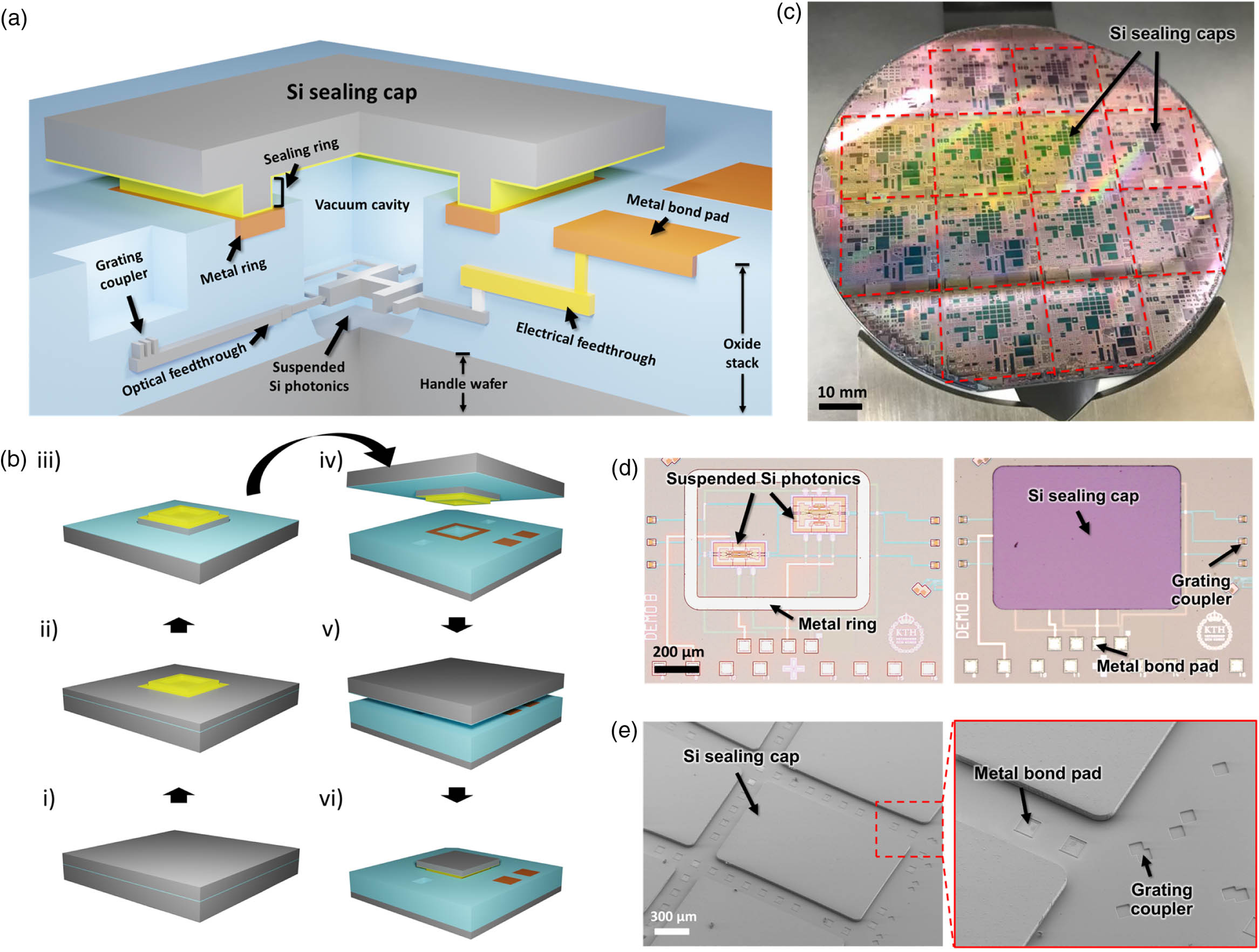
    The emerging fields of silicon (Si) photonic micro–electromechanical systems (MEMS) and optomechanics enable a wide range of novel high-performance photonic devices with ultra-low power consumption, such as integrated optical MEMS phase shifters, tunable couplers, switches, and optomechanical resonators. In contrast to conventional SiO2-clad Si photonics, photonic MEMS and optomechanics have suspended and movable parts that need to be protected from environmental influence and contamination during operation. Wafer-level hermetic sealing can be a cost-efficient solution, but Si photonic MEMS that are hermetically sealed inside cavities with optical and electrical feedthroughs have not been demonstrated to date, to our knowledge. Here, we demonstrate wafer-level vacuum sealing of Si photonic MEMS inside cavities with ultra-thin caps featuring optical and electrical feedthroughs that connect the photonic MEMS on the inside to optical grating couplers and electrical bond pads on the outside. We used Si photonic MEMS devices built on foundry wafers from the iSiPP50G Si photonics platform of IMEC, Belgium. Vacuum confinement inside the sealed cavities was confirmed by an observed increase of the cutoff frequency of the electro-mechanical response of the encapsulated photonic MEMS phase shifters, due to reduction of air damping. The sealing caps are extremely thin, have a small footprint, and are compatible with subsequent flip-chip bonding onto interposers or printed circuit boards. Thus, our approach for sealing of integrated Si photonic MEMS clears a significant hurdle for their application in high-performance Si photonic circuits.

    Gaehun Jo, Pierre Edinger, Simon J. Bleiker, Xiaojing Wang, Alain Yuji Takabayashi, Hamed Sattari, Niels Quack, Moises Jezzini, Jun Su Lee, Peter Verheyen, Iman Zand, Umar Khan, Wim Bogaerts, Göran Stemme, Kristinn B. Gylfason, Frank Niklaus. Wafer-level hermetically sealed silicon photonic MEMS[J]. Photonics Research, 2022, 10(2): A14
    Download Citation