
Feng Qiu, Yu Han. Electro-optic polymer ring resonator modulators [Invited][J]. Chinese Optics Letters, 2021, 19(4): 041301
- Chinese Optics Letters
- Vol. 19, Issue 4, 041301 (2021)
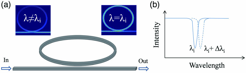
Fig. 1. (a) Schematic diagram representation of a ring resonator (top images: propagated light field of non-resonant
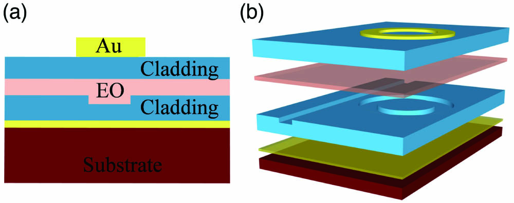
Fig. 2. (a) Cross section and (b) schematic of the ring modulators with EO polymer as the waveguide core.
Fig. 3. (a) Designed cross section of the
Fig. 4. Conceptual representation of an EO polymer/Si slot waveguide ring resonator modulator: the applied voltage drops only across the slot filled with the EO polymer, allowing a strong overlap between the electric and optic fields.
Fig. 5. (a) Cross section of the designed horizontal slot waveguide, (b) the calculated TM mode distribution, indicating a highly concentrated optical field within the EO polymer, (c) calculated electric-field distribution in the vertical-direction, and (d) device SEM image. Adapted with permission from Ref. [39].
Fig. 6. (a) Schematic of the etching-free ring resonator modulator, and (b) the fitted high resolution spectra of one resonant peak at 1549.57 nm and its spectral shift with a range of bias voltages. The shift of the resonance peak linearly fitted with the bias voltages (inset). Adapted with permission from Ref. [20].
Fig. 7. Schematic of the designed athermal ring resonator modulator: top figures are the high-frequency response (10 MHz) at different temperatures. Adapted with permission from Ref. [40].

Set citation alerts for the article
Please enter your email address
© Copyright 2018-2021 | Chinese Laser Press. All Rights Reserved 沪ICP备15018463号-20