1Key Laboratory of 3D Micro/Nano Fabrication and Characterization of Zhejiang Province, School of Engineering, Westlake University, Hangzhou 310024, China
2Institute of Advanced Technology, Westlake Institute for Advanced Study, Hangzhou 310024, China
3Interdisciplinary Graduate School of Engineering Sciences, Kyushu University, 6-1 Kasuga-koen, Kasuga, Fukuoka 816-8580, Japan
Electro-optic (EO) ring resonator modulators have a number of communications and scientific applications, including analog optical links, optical signal processing, and frequency comb generation. Among the EO materials used to fabricate ring modulators, the EO polymer has many promising characteristics, including a high EO coefficient of 100–200 pm/V (3–7 times larger than that of ), an ultrafast EO response time (), a low dielectric constant (3 to 4) with very little dispersion up to at least 250 GHz, and a straightforward spin-coating fabrication process. These inherent characteristics will be able to combine excellent EO properties with simple processing in achieving exceptional performance in a variety of high-speed optical modulation and sensing devices. This review focuses on the research and recent development of ring resonator modulators based on EO polymers. The first part describes the operation principle of EO ring resonator modulators, such as modulation mechanism, EO tunability, and 3 dB bandwidth. Subsequently, the emphasis is placed on the discussion of the ring modulators with EO polymers as the waveguide core and the improvement of EO modulation by using an EO polymer/titanium dioxide hybrid core. At the end, a series of EO polymers on silicon platforms including slot modulators, etching-free modulators, and athermal modulators are reviewed.
The world’s technological capacities to data generated by the applications like 5G, cloud computing, artificial intelligence, and internet-of-things, are quickly growing at unprecedented rates[1–5]. It creates an ever-increasing demand for transformative photonic technologies to meet the energy reduction and bandwidth enhancement challenges[6–8]. An indispensable component for the development of photonic technologies is a fast, compact, energy-efficient, broadband electro-optic (EO) modulator.
EO modulators usually have types of straight waveguide phase modulators[9], Mach–Zehnder interferometer (MZI) waveguide intensity modulators[10], and ring resonator modulators[11]. Compared with the other two structures, the advantages of ring modulators are their compact footprint, low driving voltages, and the ability to drive them as lumped RF elements to eliminate the need for the traveling-wave design. EO ring resonator modulators have a number of communications and scientific applications, including analog optical links, optical signal processing, and frequency comb generation[12]. Until now, ring resonator modulators have been realized by using silicon (Si)[13], [14], and EO polymers[11]. Si is compatible with the complementary metal–oxide–semiconductor (CMOS) process, offering the potential of photonic–electronic co-integration on large-area wafers. However, the linear EO effect (Pockels effect) is absent in bulk Si due to inversion symmetry of the crystal lattice. Hence, current Si modulators have to rely on the free-carrier plasma effect[15]. One major constraint of the free-carrier plasma effect is that the change in the real and imaginary parts of the refractive index is linked, therefore causing the modulation of only the optical phase to be difficult. In contrast, based on the linear EO effect can provide pure phase modulation at high speed, thereby enabling the generation of high-quality optical data signals based on advanced modulation formats[14]. EO polymers are also based on the linear EO effect (Pockels effect), which quantifies how the refractive index changes with the applied electric-field strength. The EO effect is a consequence of the special molecular organization of the chromophores in the EO polymer: the non-centrosymmetric structure and the abundance of delocalized electrons[16]. Compared with , EO polymers have many desirable characteristics: strong Pockels effect with high EO coefficients ();relatively low dielectric constant (3 to 4) with velocity matching between the optical and microwave signals up to at least 250 GHz;straightforward spin-coated thin-film and good compatibility with other materials and substrates.
These attractive features of EO polymers enable a variety of outstanding performances in organic or organic–inorganic hybrid waveguide modulators, such as femtojoule per bit energy consumption[17], broadband modulation up to terahertz (THz)[18], micrometers-long device[19], and etching-free fabrication technique[20]. Such successful development of EO-polymer-based modulators will benefit many photonic technologies for high-bandwidth, small-footprint, and low-energy requirements in datacom and sensing applications.
Sign up for Chinese Optics Letters TOC. Get the latest issue of Chinese Optics Letters delivered right to you!Sign up now
In this work, we will give an overview of the field of EO polymer ring resonator modulators. We will start with a brief theoretical discussion of general ring resonator properties and expand that to explore the parameters that might influence a ring modulator. Subsequently, we will pay attention to the different structures that can be used in the EO polymer ring modulators. Finally, we discuss the outlook of future development and draw some conclusions.
2. Properties of a Ring Resonator Modulator
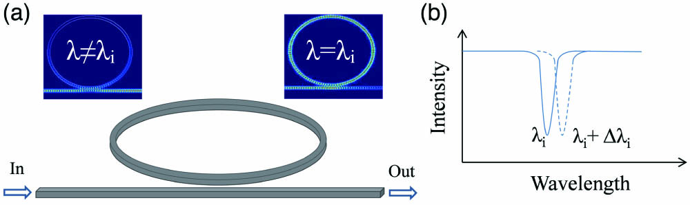
A schematic diagram of a ring resonator in its simplest form is depicted in Fig. 1, which is constructed of a ring and a straight waveguide (also called a ‘bus waveguide’). The term ring resonator is typically used to indicate any looped resonator, including not only a circular ring, but also a racetrack ring. Here, the term racetrack means that the circular shape is elongated with a straight section.
Figure 1.(a) Schematic diagram representation of a ring resonator (top images: propagated light field of non-resonant i and resonant condition i); (b) resonant spectrum of a ring modulator: the resonant peak i will have a shift i under the applied voltage.
When the gap between the ring and the bus waveguide is chosen properly (typically several hundreds of nanometers), the optical wave in the bus waveguide will be coupled into the ring. If the wavelength of the propagated light in the bus waveguide satisfies the resonant condition, that is the coupling of the wave with wavelength will be enhanced, and all others will be suppressed. As a result, only will be resonated in the ring, while the rest of the wavelengths will pass through. Here, is the effective refractive index of the bending waveguide, is the perimeter of the ring, and is an integer. When the ring waveguide is constructed of EO polymer, and some part of the light is confined in the EO polymer layer (), the resonance condition is changed by tuning the refractive index of the EO polymer, causing a shift of the resonance location. When a fixed wavelength of light is used in the waveguide, the resonance wavelength shift can be used to turn the light on and off [Fig. 1(b)]. According to Eq. (1), the resonance wavelength shift under an applied voltage on the device can be expressed as where the change of the refractive index () resulting from applied voltage is attributed to the EO polymer refractive index change (), corresponding to the in-device EO activity of the ring resonator. is expressed as where is the refractive index of EO polymer, is the EO coefficient of the EO polymer, denotes the applied voltage, and is the inter-electrode gap. In Eq. (3), is the electric field intensity E under the approximation that the direction of E is parallel to the optical field.
For an MZI modulator, half-wave voltage is used to characterize the EO performance. In contrast, for a ring modulator, it is difficult to define , because is dependent on and [21,22]. Here, is the amplitude transmission constant between the ring and the bus waveguide, and is the round-trip loss factor in the ring. Therefore, the voltage required to shift the resonance is usually used as a key figure of merit. Combining Eqs. (2) and (3), we can see that a high , a short inter-electrode gap , and a large confinement factor are preferred in order to realize a high-resonance tunability (). The extinction ratio is another important figure of merit of ring resonator modulators. For the ring structure, as shown in Fig. 1, the amplitude of the output field is given as[21]where is the round-trip phase shift, and is the amplitude of the input field. The transmission of a ring resonator is given as
When , the transmission vanishes at the resonances (), where the maximum extinction ratio is achieved. In this case, the loss in ring is equal to the coupling loss, and this condition is called a critical coupling.
Like any physical resonator, the spectral resonance peaks are not infinitely sharp, but have a finite width that is mainly affected by the scattering and bending loss of the ring waveguide[21]. In general, at a resonance wavelength , the 3 dB bandwidth of the resonance peak defines the quality factor by the relationship
This factor directly dominates the modulation bandwidth of a ring resonator modulator. The 3 dB modulation bandwidth () of a ring modulator is determined by the resistance-capacitance (RC) time and the photon lifetime as expressed by where is the cavity photon lifetime ( is the light speed in vacuum, and is the quality factor), is the contact resistance, and is the device capacitance. By utilizing a low-loss traveling-wave electrode or a simple lumped electrode for the modulator, the RF response is mainly limited by the cavity photon lifetime required to build up and release the energy from the ring resonator. Equation (6) exhibits that under the same driving voltage a narrower delivering a higher results in a larger modulation depth. Alternatively, Eq. (7) predicts that the could be limited by a larger value. Therefore, a trade-off between the bandwidth and sensitivity of the modulator must be taken into account. That is also the reason why the ring modulators with high bandwidths usually have moderate values.
3. Ring Resonator Modulators with EO Polymers as the Waveguide Core
This category of modulators usually has the waveguides that consist of an inverted ridge or a channel EO polymer core surrounded by the top and bottom claddings (as shown in Fig. 2)[22–24]. The waveguide must be single mode to provide a high extinction ratio of the modulator, so the typical thickness of the EO polymer waveguide core layer is 2–3 µm at the wavelength of 1550 nm suppressing higher-order modes. Since the refractive index () contrast is relatively low between the waveguide core () and claddings (), the bottom and top claddings usually have a thickness of 3–5 µm to avoid any absorption loss from driving metal electrodes. By using the inverted rib waveguide structure, Tazawa et al. demonstrated an EO polymer ring modulator with a 3 dB bandwidth of 7 GHz[22]. The waveguide core was made from a kind of guest-host EO polymer named AJL8/APC. The racetrack-shaped ring resonator with the bending radius of 1 mm and the straight coupling region of 150 µm was laterally coupled to a bus waveguide. The modulator had a fiber-to-fiber insertion loss of 12 dB, an extinction ratio of 14 dB, and a Q-factor of . The measured in-device was 33 pm/V. Later, by using similar inverted rib waveguide structure, the same group further improved the frequency response of a traveling-wave EO polymer ring modulator up to 84, 111, 139, and 165 GHz[12]. The 165 GHz modulation response is one of the recorded results among all kinds of ring resonator modulators.
Figure 2.(a) Cross section and (b) schematic of the ring modulators with EO polymer as the waveguide core.
Though the modulators with an EO polymer as the waveguide core have shown ultra-high frequency response, their waveguide structure generally leads to a low refractive index contrast between the core material and the claddings. Therefore, the bending radius of the polymer ring to obtain the suitable Q is usually around 1 mm, thereby limiting the miniaturization of the modulators. In order to realize a high EO coefficient, the EO polymer core must be poled efficiently, aiming at inducing a strong Pockels effect[25]. Many types of high molecular hyperpolarizability chromophores have been investigated, which show a large EO activity in the pristine films. However, such films revealed leakage of currents conceivably due to E transferring through the chromophores via higher loading concentrations. The measured electrical resistivity in the order of is often several orders lower than that of the cladding materials. In addition, the typical inter-electrode distances in such waveguides are , but the thickness of the EO core is 2–3 µm. This means that there is a large voltage in the modulator dropping across the thick cladding layers, resulting in a low poling efficiency and a high peak to peak driving voltage .
To shrink the device dimensions, shorten the inter-electrode gaps, and increase the poling efficiency, the EO polymer and titanium dioxide () hybrid core ring resonator modulators have been realized in the recent progress[11,26]. The cross section of the hybrid ring modulators is schematically shown in Fig. 3. The ring resonator modulator fabricated in that study was constructed using a thin ridge waveguide and an EO polymer cladding layer but without a traditional transparent cladding, which reduces the inter-electrode gap. At the wavelength of 1.55 µm, the refractive indices of the EO polymer, , and sol-gel were 1.61, 2.30, and 1.44, respectively. The high refractive index contrast between the EO polymer and enabled around half of the light to be confined in the EO polymer layer, but far from the top electrode. The high index contrast also minimized the ring radius down to 100 µm. The sol-gel and layers significantly blocked the excessive charge injection and reduced the leakage current during high-field poling. Moreover, since the sol-gel bottom cladding had a resistivity almost the same as that of the EO polymer, the EO polymer in the waveguide can be guaranteed with a high in-device poling efficiency and EO activity. As a result, an in-device EO coefficient of the core/EO polymer modulator was as high as 105 pm/V.
Figure 3.(a) Designed cross section of the core/EO polymer ring resonator waveguide; (b) simulated TM mode intensity distribution; (c) top view scanning electron microscopy (SEM) image of the ring structure (left: view of cross section, right: view of bus-ring gap). Adapted with permission from Ref. [11].
4. EO Polymer Hybrid to Silicon-Based Substrates Ring Resonator Modulators
The previous couple of decades have witnessed Si photonics being extensively investigated with a view to on-chip optical communications and shot-reach interconnects. Recent progress of Si modulators relying on the free-carrier plasma effect is of interest and offers a realistic means of achieving ultrafast data transfer, as a result of a careful balance among the doping configuration, loss control, and free-carriers’ lifetime[27–32]. On the other hand, the hybrid Si waveguide combination with other EO active materials is an alternative technique. In particular, utilizing an organic EO polymer creates the possibility of future powerful technologies based upon Si optical devices. In this hybrid platform, the EO effect is offered by exploiting the interaction of the guided optical mode with more precisely tailored EO polymers having a strong Pockels effect and exhibiting high EO coefficients in devices. The ultrafast response and low dielectric of polymers are notable advantages, well beyond anything that has been achieved with free-carrier plasma dispersion devices.
The primary scheme of the EO polymer/Si hybrid modulators is covering the EO layer directly on the top of a thin Si channel[33]. In the device, the TE model field intensities were tightly concentrated around Si, and there was a greater modal confinement into the EO polymer layer. Therefore, the applied electric field can induce a change in the effective index of the modulator due to the EO effect of the polymer. After poling, the resonance tunability () was , corresponding to an in-device . To further increase the resonance tunability, researchers have explored polymer/Si slot ring modulators[34,35]. In the polymer/Si slot system, as shown in Fig. 4, two Si ridges are separated from each other by a slot. This slot was typically 100–300 nm wide and filled with an EO polymer. Because of the high refractive index contrast between Si () and the EO polymer (), approximately 50% of the guiding light can be concentrated in the slot of EO polymer[36]. The EO polymer had a much higher resistivity than Si, so the two Si ridges can be used as modulator electrodes. As a result, the inter-electrode gap was ultra-small, and all of the voltages can drop on the EO polymer. According to Eqs. (2) and (3), the ultra-small gap will benefit a reduction in the high-speed driving voltage and enlarge the resonance tunability as well. The fabricated ring resonator modulators had a tunability of and a 6 dB bandwidth of 1 GHz. Despite these two existing problems associated with these modulators, the low poling efficiency of 50% () and the propagation loss as high as 35 dB/cm were afforded. In contrast, EO polymer/Si slot modulators based on the Mach–Zehnder structure have been demonstrated with a high EO activity and a much reduced optical loss[37,38]. These facts suggest that a significant improvement in tunability and further loss reduction should be possible in the polymer/Si slot ring resonator modulators.
Figure 4.Conceptual representation of an EO polymer/Si slot waveguide ring resonator modulator: the applied voltage drops only across the slot filled with the EO polymer, allowing a strong overlap between the electric and optic fields.
Expect for the above vertical slot structures, ring modulators have also been realized in horizontal slot waveguides on Si-on-insulator (SOI) substrates, as shown in Fig. 5[39]. The cross section of the horizontal slot waveguide modulator is shown in Fig. 5(a), where the horizontal slot consists of Si, EO polymer, and ridges on an SOI wafer. The confinement factor of the optical-field intensity in the EO polymer was estimated to be 58% [Fig. 5(b)]. Additionally, the TM mode overlapped little with the lateral boundaries to the ridge, so the propagation loss should be insensitive to the sidewall roughness. The fabrication was featured with the horizontal slot simply obtained by simple layered deposition, so the surfaces of the thin Si and the sputtered were smooth enough. Because of the large dielectric constant contrast of and Si to polymer, an obvious electric-field concentration in the slot was observed [Fig. 5(c)]. In this way, both optical and electric fields were well overlapped in the slot, enhancing the electric field for poling and driving modulators. The tunability of the modulator was , corresponding to an in-device of 88 pm/V. This tunability was higher than the previously reported vertical slot ring modulators[34,35] and comparable to some of the Si plasma dispersion ring modulators[13]. The 3 dB bandwidth of the horizontal slot modulator was characterized as 13.3 GHz.
Figure 5.(a) Cross section of the designed horizontal slot waveguide, (b) the calculated TM mode distribution, indicating a highly concentrated optical field within the EO polymer, (c) calculated electric-field distribution in the vertical-direction, and (d) device SEM image. Adapted with permission from Ref. [39].
Also based on SOI, a unique design of a hybrid ring resonator modulator has been presented recently, in which extra doping and etching of the SOI wafer were not required[20]. The schematic diagram and EO modulation of the device are shown in Fig. 6. The ring and adjacent bus waveguide were carved in a 300-nm-thick hydrogen silsesquioxane on p-type SOI substrate by E-beam lithography. Subsequently, the EO polymer layer and the sol-gel cladding were deposited directly by spin-coating. The fabrication of this modulator is straightforward because of the elimination of etching and additional doping of Si. Furthermore, the proposed structure results in a significant reduction of the absorption attenuation and light scattering from the waveguide sidewalls. A relatively low propagation loss of 0.6 dB/mm was measured at 1550 nm. The designed device construction was amenable in achieving high poling efficiency of the EO polymer, demonstrating a record high in-device EO coefficient of . A high-frequency test of the modulator revealed a bandwidth of 18 GHz, which is competitive with state-of-the-art plasma dispersion-based ring devices.
Figure 6.(a) Schematic of the etching-free ring resonator modulator, and (b) the fitted high resolution spectra of one resonant peak at 1549.57 nm and its spectral shift with a range of bias voltages. The shift of the resonance peak linearly fitted with the bias voltages (inset). Adapted with permission from Ref. [20].
Figure 7.Schematic of the designed athermal ring resonator modulator: top figures are the high-frequency response (10 MHz) at different temperatures. Adapted with permission from Ref. [40].
In a ring modulator, the resonant nature can enable an enhanced modulation response. However, this resonant enhancement also causes high sensitivity to ambient temperature fluctuations because of the thermo-optic (TO) effect[40]. For example, a Si ring resonator with a waveguide cross section of has a temperature-dependent wavelength shift (TDWS) of 50–80 pm/°C[41,42]. For a Si ring with a Q factor of and a resonance wavelength of , this high TDWS will break the resonance with only 2–3°C change. With tremendous growth in data traffic, an even larger amount of energy is dissipated on die. Joule losses on substrates may turn into heat, and the generated heat propagates primarily over the surface of the die. This temperature fluctuation will disrupt the designed modulation in a ring modulator. Thus, it is essential to diminish the TDWS difficulty by the utilization of an active thermal controller under the modulator, which may lead to a further power consumption problem. In contrast, the EO polymer hybrid to Si is a unique platform to resolve the thermal challenges for micro-ring resonator modulators. A TDWS as low as 2.1 pm/°C has been realized via the EO polymer hybrid to Si as shown in Fig. 7, which is 20–30 times lower than that of a pure Si ring resonator[43]. Generally, the athermal operation of the waveguide is determined by using the equation where is the TDWS, is the resonant wavelength, is the effective refractive index of the waveguide, is the substrate expansion coefficient, is the effective TO coefficient, and is the group index of the waveguide. Since the polymer has the negative TO coefficient opposite to Si’s positive coefficient, the demonstrated hybrid ring modulator is able to operate at an athermal condition. At 100 MHz, the device is demonstrated with a stable modulation over a 20–55°C temperature range. This hybrid athermal platform represents a new paradigm in modulator development and a major step towards future on-chip applications.
5. Conclusions
We have given an overview on the research and recent progress of EO polymer ring resonator modulators. Several important issues determining the driving voltage, tunability, and bandwidth of a device have been discussed. Better understanding of the operation mechanism of an EO polymer ring modulator provides a useful guideline for improving device design and fabrication to gain higher performance. As described in this review, an EO-polymer-based ring modulator not only takes advantage of optical resonances to decrease device footprint and to reduce power consumption, but also employs unique material advantages of a high EO coefficient, high bandwidth, and good compatibility with other substrates. The recent improvements in the performance of EO polymer ring modulators can lead to cost effectiveness and higher compactness in optical communication and other scientific applications.
As a future development, EO polymer ring modulator arrays can be designed to perform a number of interconnect functions and represent the key building blocks of photonic systems, not only working as active modulators/switches but also simultaneously as wavelength-selective filters. For example, an array of ring modulators can achieve modulating as well as multiplexing functions[44], which may offer great scalability for high-speed data communication through dense wavelength division multiplexing (WDM).
[5] I. Lyubomirsky, W. A. Ling. Advanced modulation for datacenter interconnect. Optical Fiber Communication Conference, W4J.3(2016).
[6] W. Mellette, P. George. Toward optical switching in the data center. 19th International Conference on High Performance Switching and Routing(2018).
[7] M. Imran, S. Haleem. Optical interconnects for cloud computing data centers: recent advances and future challenges. International Symposium on Grids and Clouds, 1(2018).
[23] B. J. Seo, S. Kim, H. Fetterman, W. Steier, D. Jin, R. Dinu. Design of ring resonators using electro-optic polymer waveguides. J. Phys. Chem., C112, 7953(2008).