• Journal of Semiconductors
  • Vol. 40, Issue 8, 081504 (2019)
Bo Gu1、2
Author Affiliations
  • 1Kavli Institute for Theoretical Sciences, and CAS Center for Excellence in Topological Quantum Computation, University of Chinese Academy of Sciences, Beijing 100190, China
  • 2Physical Science Laboratory, Huairou National Comprehensive Science Center, Beijing 101400, China
  • show less
    DOI: 10.1088/1674-4926/40/8/081504 Cite this Article
    Bo Gu. High temperature magnetic semiconductors: narrow band gaps and two-dimensional systems[J]. Journal of Semiconductors, 2019, 40(8): 081504 Copy Citation Text show less
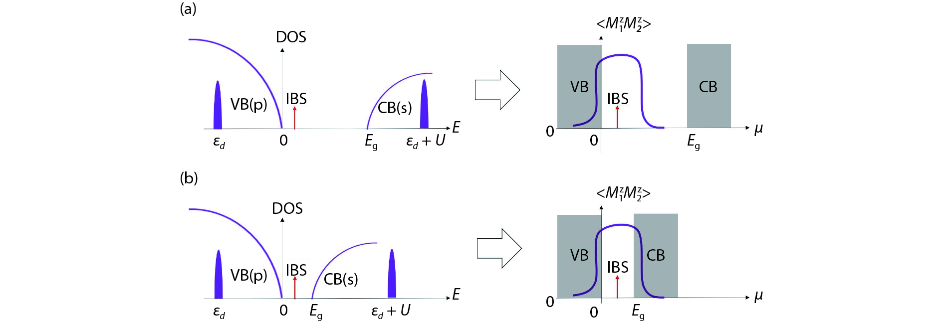
    (Color online) Schematic pictures of magnetic semiconductors with (a) wide band gaps and (b) narrow band gaps. The band gap is . The top of valence band (VB) is dominated by p orbitals, and the bottom of conduction band (CB) is dominated by s orbitals. For the impurity with d orbitals, is impurity level of d orbitals, and is the on-site Coulomb interaction. Impurity bound state (IBS) is also developed due to the doping of impurity into the host. The density of state (DOS) as a function of energy, and the magnetic correlation between two impurities as a function of the chemical potential are depicted. (a) Due to strong mixing between the impurity and the VB, the position of the IBS (arrow) is close to the top of the VB. Due to weak mixing between the impurity and the CB, usually no IBS appears below the bottom of the CB[19–21]. Thus, we have 0 for the wide band gap case. By the condition , positive (FM coupling) can develop[22–24]. For p-type carriers (), ferromagnetic coupling can be obtained as the condition can be satisfied. For n-type carriers (), no magnetic coupling is obtained between impurities because the condition cannot be satisfied[19–21]. (b) Case for narrow band gap . By choosing suitable host semiconductors and impurities, the condition 0 can be obtained. For both p-type and n-type carriers, ferromagnetic coupling can be obtained because the condition is satisfied.
    Fig. 1. (Color online) Schematic pictures of magnetic semiconductors with (a) wide band gaps and (b) narrow band gaps. The band gap is . The top of valence band (VB) is dominated by p orbitals, and the bottom of conduction band (CB) is dominated by s orbitals. For the impurity with d orbitals, is impurity level of d orbitals, and is the on-site Coulomb interaction. Impurity bound state (IBS) is also developed due to the doping of impurity into the host. The density of state (DOS) as a function of energy, and the magnetic correlation between two impurities as a function of the chemical potential are depicted. (a) Due to strong mixing between the impurity and the VB, the position of the IBS (arrow) is close to the top of the VB. Due to weak mixing between the impurity and the CB, usually no IBS appears below the bottom of the CB[1921]. Thus, we have 0 for the wide band gap case. By the condition , positive (FM coupling) can develop[2224]. For p-type carriers ( ), ferromagnetic coupling can be obtained as the condition can be satisfied. For n-type carriers ( ), no magnetic coupling is obtained between impurities because the condition cannot be satisfied[1921]. (b) Case for narrow band gap . By choosing suitable host semiconductors and impurities, the condition 0 can be obtained. For both p-type and n-type carriers, ferromagnetic coupling can be obtained because the condition is satisfied.
    (Color online) Band structure of the ZnO host with wurtzite, zincblende, and rocksalt crystal structures. Adapted from Ref. [19].
    Fig. 2. (Color online) Band structure of the ZnO host with wurtzite, zincblende, and rocksalt crystal structures. Adapted from Ref. [19].
    (Color online) For Mn impurity in ZnO, hybridization parameter of a Mn orbital with the valence bands and the conduction bands. Adapted from Ref. [19].
    Fig. 3. (Color online) For Mn impurity in ZnO, hybridization parameter of a Mn orbital with the valence bands and the conduction bands. Adapted from Ref. [19].
    (Color online) For Mn impurity in ZnO, square of the magnetic moment at the impurity site as a function of the chemical potential . The top of valence is energy zero, and the bottom of the conduction band is noted as vertical dashed lines. Adapted from Ref. [19].
    Fig. 4. (Color online) For Mn impurity in ZnO, square of the magnetic moment at the impurity site as a function of the chemical potential . The top of valence is energy zero, and the bottom of the conduction band is noted as vertical dashed lines. Adapted from Ref. [19].
    (Color online) For Mn impurity in ZnO, impurity-impurity magnetic correlation function as a functino of distance between two impurities for the wurtzite, zincblende, and rocksalt structures. is lattice constant. Adapted from Ref. [19].
    Fig. 5. (Color online) For Mn impurity in ZnO, impurity-impurity magnetic correlation function as a functino of distance between two impurities for the wurtzite, zincblende, and rocksalt structures. is lattice constant. Adapted from Ref. [19].
    (Color online) For N impurity in MgO, host band and hybridization. (a) MgO bands structure, where an direct band gap of 7.5 eV was obtained. Hybridization between 2orbitals of N and (b) valence bands and (c) conduction bands of MgO. Adapted from Ref. [21].
    Fig. 6. (Color online) For N impurity in MgO, host band and hybridization. (a) MgO bands structure, where an direct band gap of 7.5 eV was obtained. Hybridization between 2 orbitals of N and (b) valence bands and (c) conduction bands of MgO. Adapted from Ref. [21].
    (Color online) For N impurity in MgO, square of magnetic moment as a function of chemical potential . Adapted from Ref. [21].
    Fig. 7. (Color online) For N impurity in MgO, square of magnetic moment as a function of chemical potential . Adapted from Ref. [21].
    (Color online) For N impurity in MgO, impurity-impurity magnetic correlation as a function of distance , for the impurity level (a) = – eV and (b) = – eV. Adapted from Ref. [21].
    Fig. 8. (Color online) For N impurity in MgO, impurity-impurity magnetic correlation as a function of distance , for the impurity level (a) = – eV and (b) = – eV. Adapted from Ref. [21].
    (Color online) For Mn impurity in BaZn2As2, host band and impurity-host hybridization. (a) Energy bands off host BaZn2As2. Band gap of 0.2 eV was obtained by DFT calculations, consistent with experiment[11]. The hybridization parameter between the 3d orbitals of Mn and (b) valence bands and (c) conduction bands of BaZn2As2. Adapted from Ref. [17].
    Fig. 9. (Color online) For Mn impurity in BaZn2As2, host band and impurity-host hybridization. (a) Energy bands off host BaZn2As2. Band gap of 0.2 eV was obtained by DFT calculations, consistent with experiment[11]. The hybridization parameter between the 3d orbitals of Mn and (b) valence bands and (c) conduction bands of BaZn2As2. Adapted from Ref. [17].
    (Color online) For Mn impurity in BaZnAs, chemical potential dependence of (a) impurity occupation number of , and (b) magnetic correlation between impurities of the first-nearest neighbor. The band gap of 0.2 eV is noted by dash lines. Adapted from Ref. [17].
    Fig. 10. (Color online) For Mn impurity in BaZn As , chemical potential dependence of (a) impurity occupation number of , and (b) magnetic correlation between impurities of the first-nearest neighbor. The band gap of 0.2 eV is noted by dash lines. Adapted from Ref. [17].
    (Color online) For Mn impurities in BaZnAs, magnetic correlation as a function of distance . (a) Chemical potential is set as = –0.3 eV to model p-type case. (b) It is set as = 0.15 eV for n-type case. The first, second, and third nearest neighbors of are noted. Adapted from Ref. [17].
    Fig. 11. (Color online) For Mn impurities in BaZn As , magnetic correlation as a function of distance . (a) Chemical potential is set as = –0.3 eV to model p-type case. (b) It is set as = 0.15 eV for n-type case. The first, second, and third nearest neighbors of are noted. Adapted from Ref. [17].
    (Color online) Cr impurity versus Mn impurity in host BaZnAs. Chemical potential dependence of (a) impurity occupation number , and (b) magnetic correlation between impurities of the 1st nearest neighbor. Adapted from Ref. [18].
    Fig. 12. (Color online) Cr impurity versus Mn impurity in host BaZn As . Chemical potential dependence of (a) impurity occupation number , and (b) magnetic correlation between impurities of the 1st nearest neighbor. Adapted from Ref. [18].
    (Color online) For Cr impurity in BaZnAs, magnetic correlation as a function of the distance . (a) chemical potential is set as = –0.1 eV to model p-type case. (b) It is set as = 0.15 eV for n-type case. The first, second, and third nearest neighbors of are noted. Adapted from Ref. [18].
    Fig. 13. (Color online) For Cr impurity in BaZn As , magnetic correlation as a function of the distance . (a) chemical potential is set as = –0.1 eV to model p-type case. (b) It is set as = 0.15 eV for n-type case. The first, second, and third nearest neighbors of are noted. Adapted from Ref. [18].
    (Color online) Crystal structure of two-dimensional CrGeSe.
    Fig. 14. (Color online) Crystal structure of two-dimensional Cr Ge Se .
    (Color online) Electron band structure of two-dimensional CrGeSe, obtained by the density functional theory calculations. Adapted from Ref. [39].
    Fig. 15. (Color online) Electron band structure of two-dimensional Cr Ge Se , obtained by the density functional theory calculations. Adapted from Ref. [39].
    (Color online) For two-dimensional CrGeSewith different tensile strains, the normalized magnetization as a function temperature. Adapted from Ref. [39].
    Fig. 16. (Color online) For two-dimensional Cr Ge Se with different tensile strains, the normalized magnetization as a function temperature. Adapted from Ref. [39].
    (Color online) Crystal structure of two-dimensional PtBr.
    Fig. 17. (Color online) Crystal structure of two-dimensional PtBr .
    (Color online) The band structure of two-dimensional PdBr, where Chern number C of the nontrivial band near Fermi energy is indicated, and the band gap is = 28.1 meV. The result is obtained by the density functional theory calculation. Adapted from Ref. [40].
    Fig. 18. (Color online) The band structure of two-dimensional PdBr , where Chern number C of the nontrivial band near Fermi energy is indicated, and the band gap is = 28.1 meV. The result is obtained by the density functional theory calculation. Adapted from Ref. [40].
    (Color online) For two-dimensional PtBr,temperature dependence of the normalized magnetic moment obtained by the Monte Carlo simulation and the density functional theory calculation. Adapted from Ref. [40].
    Fig. 19. (Color online) For two-dimensional PtBr ,temperature dependence of the normalized magnetic moment obtained by the Monte Carlo simulation and the density functional theory calculation. Adapted from Ref. [40].
    Bo Gu. High temperature magnetic semiconductors: narrow band gaps and two-dimensional systems[J]. Journal of Semiconductors, 2019, 40(8): 081504
    Download Citation