Abstract
Magnetic semiconductors have been demonstrated to work at low temperatures, but not yet at room temperature for spin electronic applications. In contrast to the p-type diluted magnetic semiconductors, n-type diluted magnetic semiconductors are few. Using a combined method of the density function theory and quantum Monte Carlo simulation, we briefly discuss the recent progress to obtain diluted magnetic semiconductors with both p- and n-type carriers by choosing host semiconductors with a narrow band gap. In addition, the recent progress on two-dimensional intrinsic magnetic semiconductors with possible room temperature ferromangetism and quantum anomalous Hall effect are also discussed.1. Introduction
Spin electronics is a rapidly developing interdisciplinary subject in condensed matter physics. Electrons have two intrinsic properties: charge and spin. Traditional electronic devices, through the regulation of electronic charge to achieve a variety of functions, with the continuous enhancement of performance, the size of the device is decreasing, has been close to the physical limit of atomic scale. In order to surpass the traditional electronic devices, the research on how to regulate the spin electronics of electron spin has been developed gradually, and many novel physical phenomena and new materials have been produced, such as giant magnetoresistance, tunnel magnetoresistance, magnetic semiconductor, spin Hall effect, quantum spin Hall effect, quantum anomalous Hall effect, topological insulator, etc.[1, 2].
The development history of condensed matter physics shows that the in-depth study of novel physical phenomena is helpful to deepen our understanding of condensed state physics and expand the boundary of condensed matter physics. It is of great significance in basic science and practical application. A typical example is giant magnetoresistance discovered in the 1988, which, with the deepening of research, has triggered the revolution of large capacity and miniaturization of hard disks. It has been widely used in high-density readout head and magnetic storage elements, and has become the standard technology of computer hard disks. However, many novel physical phenomena in spin electronics have not been applied in practice at present. An important constraint is that some novel physical phenomena are observed only at low temperatures in the laboratory, and the practical application requires that such physical phenomena can be realized at room temperature.
An important material is the magnetic semiconductor, which urgently needs to improve the temperature of its realization. Magnetic semiconductors, which combine the two important areas of magnetism and semiconductors, have been widely studied and are a basic material for the realization of spin electronics devices. The practical application requires that the ferromagnetic Curie temperature of magnetic semiconductors be higher than that of room temperature. Can we create magnetic semiconductors that work at room temperature? It is one of the 125 unknown scientific problems listed by Science in 2005[3]. Although some research articles claim to have been experimentally obtained for ferromagnetic semiconductors at room temperature, so far, room temperature ferromagnetic semiconductors, which have been widely repeated and widely accepted, have not been obtained yet.
The most extensive and in-depth study of magnetic semiconductor materials is (Ga,Mn)As[4, 5]. The present record of its Curie temperature
is about 200 K, which was created in 2011 by Institute of Semiconductors in Chinese Academy of Sciences[6]. A lot of difficulties have been encountered when trying to raise the Curie temperature of (Ga,Mn)As. The binary Mn ion is replaced with the trivalent Ga ion, and the magnetic moment and the hole carrier are introduced at the same time. Therefore, (Ga,Mn)As as a p-type magnetic semiconductor. The mismatch of the valence of manganese and gallium ions leads to severe and limited chemical solubility for the Mn in GaAs. In addition, because of the simultaneous doping of carriers and magnetic moments, it is difficult to turn the charge carriers and magnetism to its optimized condition separately. Therefore, there is an urgent need for new ideas and materials to explore room temperature magnetic semiconductors.
In order to solve the above difficulties, Li(Zn,Mn)As, regarded as I–II–V magnetic semiconductor, was proposed in the calculation[7], and later manufactured in the experiment with
= 50 K[8]. By isovalent (Zn2+, Mn2+) substitution, spin is introduced. By tuning excess or deficient Li concentration, the carrier can be controlled independently. Although Li(Zn,Mn)As with excess Li+ is considered to be a promising n-type magnetic semiconductor, p-type carriers were obtained in the experiment. The introduction of the hole is probably due to the excess Li+ in substitutional Zn2+ sites[8]. In Li(Zn,Mn)P, another I–II–V magnetic semiconductor,
= 34 K is obtained in the experiment[9]. In the experiment, Li(Zn,Mn)P with excess Li was also identified as p-type, due to the same reason as that for Li(Zn,Mn)As[9]. A 1111-type magnetic semiconductor (
)(
)AsO was reported with
= 40 K in the experiment [10]. Although these p-type magnetic semiconductors have some obvious advantages over (Ga,Mn)As, the obtained
is much lower than that of (Ga,Mn)As.
The
up to 230 K was achieved in another type of magnetic semiconductor (Ba,K)(Zn,Mn)
As
, which was created by the experimental group in Institute of Physics in Chinese Academy of Sciences in 2013[11, 12]. The magnetic moment is doped with isovalent (Zn2+, Mn2+) substitutions, and p-type carriers is introduced by (Ba2+, K+) substitutions. Driven by high
, the density functional theory calculations[13] and photoemission spectroscopy experiments [14, 15] were conducted to understand the mechanism of ferromagnetism in p-type (Ba,K)(Zn,Mn)
As
.
The evidence of n-type ferromagnetic semiconductor was obtained in the Co doped semiconductor Ba(Zn,Co)
As
with Curie temperature of 45 K fabricated by the experimental group of Zhejiang University in 2019[16]. Both n-type carriers and spins are introduced due to the doping of Co.
Inspired by the above experimental progress, we proposed a new direction to obtain high temperature magnetic semiconductor by considering the magnetic semiconductors with narrow band gaps in 2016[17, 18]. Unlike the wide band gap magnetic semiconductors represented by (Ga,Mn) as, which have been studied extensively over the past 20 years, our calculations show that narrow band gap semiconductors are more likely to host both p- and n-type magnetic semiconductors. Because narrow band gap semiconductor is favored to form the shallow impurity levels, which is extended and can mediate ferromagnetic coupling between magnetic impurities in both p- and n-type carriers. The high Curie temperatures can also be expected due to long-range ferromagnetic coupling.
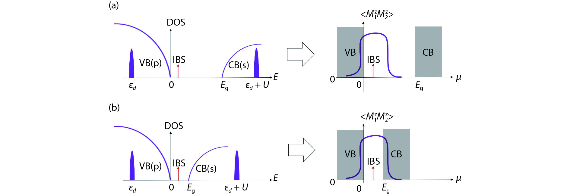
A schematic diagram describing magnetic semiconductors with wide band gap is shown in Fig. 1(a). In the studies of magnetic semiconductors with wide band gap E, such as (Zn,Mn)O[19], (Ga,Mn)As[20], and Mg(O,N)[21], the impurity bound state (IBS)
was obtained close to the top of the valence band (VB), and usually no IBS is obtained below the bottom of the conduction band (CB). The ferromagnetic correlation (positive)
between two impurities can be obtained when the chemical potential
and IBS satisfy the relation
[22, 23, 24]. For p-type carriers (
), such relation can be satisfied, and the ferromagnetic coupling is obtained. For n-type carriers (
), such relation cannot be satisfied, and no magnetic coupling is obtained.
![(Color online) Schematic pictures of magnetic semiconductors with (a) wide band gaps and (b) narrow band gaps. The band gap is . The top of valence band (VB) is dominated by p orbitals, and the bottom of conduction band (CB) is dominated by s orbitals. For the impurity with d orbitals, is impurity level of d orbitals, and is the on-site Coulomb interaction. Impurity bound state (IBS) is also developed due to the doping of impurity into the host. The density of state (DOS) as a function of energy, and the magnetic correlation between two impurities as a function of the chemical potential are depicted. (a) Due to strong mixing between the impurity and the VB, the position of the IBS (arrow) is close to the top of the VB. Due to weak mixing between the impurity and the CB, usually no IBS appears below the bottom of the CB[19–21]. Thus, we have 0 for the wide band gap case. By the condition , positive (FM coupling) can develop[22–24]. For p-type carriers (), ferromagnetic coupling can be obtained as the condition can be satisfied. For n-type carriers (), no magnetic coupling is obtained between impurities because the condition cannot be satisfied[19–21]. (b) Case for narrow band gap . By choosing suitable host semiconductors and impurities, the condition 0 can be obtained. For both p-type and n-type carriers, ferromagnetic coupling can be obtained because the condition is satisfied.](/Images/icon/loading.gif)
Figure 1.(Color online) Schematic pictures of magnetic semiconductors with (a) wide band gaps and (b) narrow band gaps. The band gap is
. The top of valence band (VB) is dominated by p orbitals, and the bottom of conduction band (CB) is dominated by s orbitals. For the impurity with d orbitals,
is impurity level of d orbitals, and
is the on-site Coulomb interaction. Impurity bound state (IBS) is also developed due to the doping of impurity into the host. The density of state (DOS) as a function of energy, and the magnetic correlation
between two impurities as a function of the chemical potential
are depicted. (a) Due to strong mixing between the impurity and the VB, the position of the IBS
(arrow) is close to the top of the VB. Due to weak mixing between the impurity and the CB, usually no IBS appears below the bottom of the CB[19–21]. Thus, we have 0
for the wide band gap case. By the condition
, positive (FM coupling)
can develop[22–24]. For p-type carriers (
), ferromagnetic coupling can be obtained as the condition
can be satisfied. For n-type carriers (
), no magnetic coupling is obtained between impurities because the condition
cannot be satisfied[19–21]. (b) Case for narrow band gap
. By choosing suitable host semiconductors and impurities, the condition 0
can be obtained. For both p-type and n-type carriers, ferromagnetic coupling can be obtained because the condition
is satisfied.
The situation changes for the magnetic semiconductors with narrow band gaps, as shown in Fig. 1(b). After selecting suitable host semiconductors and impurities, the relation 0
can be obtained. As a result, for both the p- and the n-type carriers, the condition
is satisfied, and the ferromagnetic coupling can be expected.
Another possible direction to obtain high temperature magnetic semiconductors is van der Waals two-dimensional (2D) magnetic semiconductors. In 2017, Ising-type ferromagnetism was observed in monolayer CrI
in experiment with Curie temperature
= 45 K[25]. In the same year, 2D magnetic semiconductor Cr
Ge
Te
was obtained in experiment with
= 28 K[26]. In 2018, two experimental teams declared that the single-layers VSe
[27] and MnSe
[28] have the Curie temperatures higher than room temperature.
In the following, we introduce our combined method of the density function theory and quantum Monte Carlo simulation (DFT + QMC). It was applied to study the magnetic semiconductors. For the cases with wide band gaps, Mn-doped ZnO and N-doped MgO are discussed. For the cases with narrow band gaps, Mn- and Cr-doped BaZn
As
are discussed. In addition, the recently growing 2D magnetic semiconductors are also mentioned.
2. DFT + QMC method
There are two kinds of objects in magnetic semiconductors: one is the itinerant carriers, the other is the localized impurities. The itinerant carriers, which experience the periodic crystal potential and give rise to a k-dependent energy (i.e., electronic band structure), can be reasonably described by the mean-field theory, such as the density functional theory (DFT)[29, 30]. The localized impurities, which are determined by the on-site Coulomb interaction, can be correctly described by the non-perturbative theory, such as the Hirsch–Fye quantum Monte Carlo (QMC) technique[31].
In order to accurately describe these two kinds of objects in real materials by a unified theoretical framework, we proposed a combined DFT + QMC method. First, the one-particle parts of the Anderson impurity model are formulated within the DFT or tight-binding approximation for determining the host band structure and the impurity-host hybridization. Second, the correlation parts of the Anderson impurity model at finite temperatures are calculated by the QMC method. For the case of singlet impurity, we can calculate the impurity bound state in the band gap, the magnetic susceptibility, the occupations number, the impurity-host magnetic correlations. For the case of multi-impurities, we can calculate the magnetic correlations between any orbitals and any positions of impurities. Our combined DFT + QMC method has been applied for designing functional semiconductors[19–21] and metals[32–34].
The Anderson impurity model[35] is defined as:
$\begin{split}
H & = \sum\limits_{{k},\alpha,\sigma}[\epsilon_{\alpha}({ k})-\mu] c^{\dagger}_{{k}\alpha\sigma}c_{{k}\alpha\sigma} \;\\
& \quad +\sum\limits_{{k},\alpha,{i},\xi,\sigma}(V_{{i}\xi{ k}\alpha } d^{\dagger}_{{i}\xi\sigma} c_{{k}\alpha\sigma} + h.c.) \;\\
& \quad +(\varepsilon_{d}-\mu)\sum\limits_{{i},\xi,\sigma} d^{\dagger}_{{i}\xi\sigma}d_{{i}\xi\sigma} + U\sum\limits_{{i},\xi}n_{{i}\xi\uparrow}n_{{i}\xi\downarrow}.
\end{split}$
(1)
and
are the creation and annihilation operators for host electrons, respectively.
is wave vector, and
is spin of host electrons.
denotes valence band, and
the conduction band.
is host electron band.
is chemical potential.
and
are the creation and annihilation operators of impurity localized electron, respectively. Impurity site is
, orbital is
, and spin is
. Impurity occupation number is defined as
. Hybridization between the impurity and the host is
. The energy level of impurity
orbital is
. The on-site Coulomb repulsion of the impurity is
. The single-orbital approximation is used, i.e. Hund coupling
is neglected, to describe the magnetic sates of impurities.
The hybridization matrix element between the impurity and the host is expressed as
, which can be obtained as
$ V_{\xi\alpha }({ k}) = \sum\limits_{o,{n}}{\rm e}^{i { k}\cdot ({ n}-{ i})}a_{\alpha o}({ k}) \langle\varphi_{\xi}({ i})|H|\varphi_{o}({ n})\rangle. $ (2)
is impurity
state at site
.
is host state with band index
and wave vector
. It is expanded by atomic orbitals
with orbital index
, site index
, expansion coefficient
. Total number of host lattice sites is
. To calculate the matrix element
, the DFC calculation based on a supercell is needed.
With parameters obtained by DFT calculations, magnetic correlations of the impurities can be calculated using the Hirsch-Fye QMC technique. The operators of
component of magnetic moment
and impurity occupation number
are defined, respectively,
$ M^z_{{i}\xi} = n_{{i}\xi\uparrow} - n_{{i}\xi\downarrow}, $ (3)
$ n_{{i}\xi} = n_{{i}\xi\uparrow} + n_{{i}\xi\downarrow}, $ (4)
where
is orbital of impurity,
is impurity site,
is spin-up, and
is spin-down.
3. Diluted magnetic semiconductors with wide band gaps
3.1. (Zn,Mn)O
As an example of diluted magnetic semiconductors with wide band gaps, we discuss the ferromagnetism in the compound Mn-doped ZnO[19].
For ZnO, the wurtzite structure is the most common phase. In thin films, the zincblende structure is stable. At high pressure, the rocksalt structure is also experimentally possible. The band structures of ZnO with the wurtzite, zinc-blende, and rocksalt structures can be calculated using the tight-binding parameters, as shown in Figs. 2(a)–2(c), respectively. For the wurtzite and zincblende structures, a direct gap of 3.45 eV is obtained. For the rocksalt structure, an indirect semiconductor gap is obtained.
Figure 2.(Color online) Band structure of the ZnO host with wurtzite, zincblende, and rocksalt crystal structures. Adapted from Ref. [19].
For Mn-doped ZnO, the hybridization parameter
between the Mn impurity and the host Zn is plotted in Fig. 3. It is noted that the hybridization vanish at the
point for the rocksalt structure, and hybridization value at the
point for zincblende structure is larger than that for wurtzite structure.
Figure 3.(Color online) For Mn impurity in ZnO, hybridization parameter
of a Mn
orbital with the valence bands and the conduction bands. Adapted from Ref. [19].
Figs. 4(a) and 4(b) shows square of the magnetic moment at the impurity site
as a function of chemical potential
for Mn-doped in ZnO. The presence of a discontinuity in
versus
are observed, which denotes the existence of an impurity bound state (IBS) at this energy. For (Zn,Mn)O, the shallow IBS with position
0.1 eV and
0.2 eV are obtained for the zinblende and wurtzite structures, respectively. A much deeper IBS with position
eV is found with rocksalt structure. In addition, no IBS is found near the bottom of conduction band for all three structures.
Figure 4.(Color online) For Mn impurity in ZnO, square of the magnetic moment at the impurity site
as a function of the chemical potential
. The top of valence is energy zero, and the bottom of the conduction band is noted as vertical dashed lines. Adapted from Ref. [19].
Impurity–impurity magnetic correlation function
as a function of impurity separation
is shown in Fig. 5.
is the lattice constant. For wurtzite structure, ferromagnetic correlation between Mn impurities is obtained with chemical potential
. The range of the ferromagnetic correlation becomes longer with
= 0.15 eV. Ferromagnetic correlations becomes weaker with further increasing
. Similar results are obtained for the zincblende structure, as shown in Fig. 5(b). A longer range of ferromagnetic correlations is obtained in zincblende structure than that in wurtzite structure. No magnetic correlations is obtained for the rocksalt structure, as shown in Fig. 5(c). This is due to the fact that the IBS of rocksalt structure is too deep, as seen in Fig. 4. These results show that, for shallow IBS, the ferromagnetic interaction between impurities can be obtained as the condition
is satisfied.
Figure 5.(Color online) For Mn impurity in ZnO, impurity-impurity magnetic correlation function
as a functino of distance
between two impurities for the wurtzite, zincblende, and rocksalt structures.
is lattice constant. Adapted from Ref. [19].
3.2. type Mg(O,N)
As another example of diluted magnetic semiconductors with wide band gap, we discuss the ferromagnetism in the compound N-doped MgO, which is the so-called
magnetic semiconductors [21].
MgO has a rocksalt structure. The band structure of MgO is shown in Fig. 6(a). The bottom of conduction band is dominated by
orbital of Mg, and the top of valence bands mainly comes from the
orbitals of O. At the
point, a very wide band gap of 7.5 eV is obtained.
Figure 6.(Color online) For N impurity in MgO, host band and hybridization. (a) MgO bands structure, where an direct band gap of 7.5 eV was obtained. Hybridization between 2
orbitals of N and (b) valence bands and (c) conduction bands of MgO. Adapted from Ref. [21].
The hybridization at the
point between
orbital of N impurity and valence bands of MgO is finite, while that with conduction band is zero. Since the gap edge of MgO is at
point, the hybridization value near
will be important. Due to the mixing between impurity and host, an impurity bound state may appear in the gap.
The square of magnetic moment
as a function of chemical potential
is shown in Fig. 7. Sharp increases in the magnitude of
are observed, around the energy of
eV for the impurity
energy
eV, and around the energy of
eV for
eV. Near the bottom of the conduction band, no such sharp variation is observed. As shown in Fig. 6, the hybridization with conduction band are around zero at
, much weaker than the hybridization with valence bands. The IBS is expected at the energy of sharp increase (or decrease) in
as a function of
.
Figure 7.(Color online) For N impurity in MgO, square of magnetic moment
as a function of chemical potential
. Adapted from Ref. [21].
The magnetic correlation function
of
orbitals of N as a function of impurity separation
is studied, and the results are shown in Fig. 8.
is lattice constant. For impurity energy
eV, ferromagnetic correlations are obtained at chemical potential
eV. For
eV, the IBS lies about 0.08 eV in the gap, as shown in Fig. 7. For
to 0.06 eV, ferromagnetic correlations become larger and longer. These results confirmed that, like what we obtained in Mn-doped ZnO case, for shallow IBS the ferromagnetic interaction between impurities can develop as the condition
is satisfied.
Figure 8.(Color online) For N impurity in MgO, impurity-impurity magnetic correlation
as a function of distance
, for the impurity level (a)
= –
eV and (b)
= –
eV. Adapted from Ref. [21].
4. Diluted magnetic semiconductors with narrow band gaps
4.1. Ba(Zn,Mn)2As2
As an example of diluted magnetic semiconductors with narrow band gaps, we discuss the ferromagnetism in the compound Mn-doped BaZn
As
[17].
By using the Wien2k package[36], we calculate the band structure
and hybridization parameters
, as shown in Fig. 9. By the modified Beck–Johnson exchange potential (mBJ) [37], the gap band
= 0.2 eV is obtained. It is consistent with previous calculations[14, 38] and experimental value[11].
Figure 9.(Color online) For Mn impurity in BaZn2As2, host band and impurity-host hybridization. (a) Energy bands off host BaZn2As2. Band gap of 0.2 eV was obtained by DFT calculations, consistent with experiment[11]. The hybridization parameter between the 3d orbitals of Mn and (b) valence bands and (c) conduction bands of BaZn2As2. Adapted from Ref. [17].
For Mn impurity in BaZn
As
, the impurity occupation number
as a function of chemical potential
is shown in Fig. 10(a). The top of valence band is set as 0, and the bottom of conduction band is set as 0.2 eV. Sharp increases in
are observed. For the orbitals
=
,
,
, and
, the IBS exists at energy
, and 0.0 eV, respectively. Magnetic correlation
between impurities of the first-nearest neighbor is shown in Fig. 10(b).
Figure 10.(Color online) For Mn impurity in BaZn
As
, chemical potential
dependence of (a) impurity occupation number
of
, and (b) magnetic correlation
between impurities of the first-nearest neighbor. The band gap of 0.2 eV is noted by dash lines. Adapted from Ref. [17].
For Mn impurities in BaZn
As
, we study the magnetic correlation
as a function of the distance
. For p-type carriers, we take
eV as shown in Fig. 11(a). Long-range ferromagnetic coupling is obtained for the orbitals
=
and
. For n-type n-type carriers, we take
= 0.15 eV as shown in Fig. 11(b). Long-range ferromagnetic coupling is obtained for the orbitals
=
and
. It is observed that the ferromagnetic interaction between impurities can develop as the condition
is satisfied, when IBS is close to the band edges.
Figure 11.(Color online) For Mn impurities in BaZn
As
, magnetic correlation
as a function of distance
. (a) Chemical potential is set as
= –0.3 eV to model p-type case. (b) It is set as
= 0.15 eV for n-type case. The first, second, and third nearest neighbors of
are noted. Adapted from Ref. [17].
4.2. Ba(Zn,Cr)2As2
As other example of magnetic semiconductor with narrow band gap, we discuss the ferromagnetism in the compound Cr-doped BaZn
As
[18].
In host BaZn
As
, let us compare the ferromagnetic coupling due to Cr impurities and that due to Mn impurities. The position of IBS of Cr impurity is closer to the bottom of the conduction band than that of the Mn impurity, as shown in Fig. 12(a). This is reasonable, since the energy level of Cr impurity is higher than that of the Mn impurity. The magnetic correlation
between two impurities with the 1st nearest neighbor is shown in Fig. 12(b). For n-type carrier with
0.2 eV, the ferromagnetic correlation for the Cr impurity is expected. It is more promising than that for the Mn impurity.
Figure 12.(Color online) Cr impurity versus Mn impurity in host BaZn
As
. Chemical potential
dependence of (a) impurity occupation number
, and (b) magnetic correlation
between impurities of the 1st nearest neighbor. Adapted from Ref. [18].
For Cr impurities in BaZn
As
, we study the magnetic correlation
as a function of the distance
. For p-type carriers, we take
= –0.1 eV as shown in Fig. 13(a). Long-range ferromagnetic coupling is obtained for the orbital
=
. For n-type carriers, we take
= 0.15 eV as shown in Fig. 13(b). Long-range ferromagnetic coupling is obtained for the orbitals
=
and
. It is observed that the ferromagnetic interaction between impurities can develop as the condition
is satisfied, for both p- and -type carriers.
Figure 13.(Color online) For Cr impurity in BaZn
As
, magnetic correlation
as a function of the distance
. (a) chemical potential is set as
= –0.1 eV to model p-type case. (b) It is set as
= 0.15 eV for n-type case. The first, second, and third nearest neighbors of
are noted. Adapted from Ref. [18].
5. Two-dimensional magnetic semiconductors
5.1. Cr2Ge2Se6
As an example of 2D magnetic semiconductors, we discussed our recent work on Cr
Ge
Te
, which was predicted to have room temperature
by applying a few percent strain[39].
The structure of the Cr
Ge
Se
monolayer is depicted in Fig. 14, whose space group is
(No.162). The band structure of Cr
Ge
Se
is obtained by DFT calculation, as shown in Fig. 15. A band gap of 0.748 eV is observed.
Figure 14.(Color online) Crystal structure of two-dimensional Cr
Ge
Se
.
Figure 15.(Color online) Electron band structure of two-dimensional Cr
Ge
Se
, obtained by the density functional theory calculations. Adapted from Ref. [39].
For monolayer Cr
Ge
Se
, the normalized magnetization as a function of temperature is obtained by the Monte Carlo simulation and the DFT calculation, as shown in Fig. 16. The calculated Curie temperature for 2D Cr
Ge
Se
is
= 144 K. The Curie temperature can be enhanced to
= 326 K by applying 3
tensile strain, and
= 500 K with 7% tensile strain, as shown in Fig. 16. For 3% tensile strain, the volume cell increases 9%. Our result predicts that 2D Cr
Ge
Se
by applying a few percent strain can be a promising candidate for room-temperature ferromagnetic semiconductor.
Figure 16.(Color online) For two-dimensional Cr
Ge
Se
with different tensile strains, the normalized magnetization as a function temperature. Adapted from Ref. [39].
5.2. PtBr3
As another example of 2D magnetic semiconductors, we discussed our recent work on PtBr
, which was predicted to have room temperature
with quantum anomalous Hall effect (QAHE) [40].
PtBr
monolayer has space group
(No.162), and the structure is depicted in Fig. 17. Due to crystal field, the d orbitals Pt are split into threefold t and twofold e orbitals, where energy of e orbitals is higher than that of
orbitals. Pt3+ has seven 5
electrons, six electrons occupied
orbitals, and one fill e orbitals. So, spin at Pt site is
.
Figure 17.(Color online) Crystal structure of two-dimensional PtBr
.
The band structure of PtBr
monolayers is calculated by the DFT method, as shown in Fig. 18. A band gap
= 28.1 meV is obtained for PtBr
monolayer due to the spin-orbit coupling.
is higher than room temperature. On the other hand, topologically nontrivial band structure is characterized by a nonzero Chern number C, which counts the number of edge states. For the band just below the Fermi level, its Chern number C obtained by integrating the Berry curvature over the BZ is 1, as shown by a line with red color in Fig. 18.
Figure 18.(Color online) The band structure of two-dimensional PdBr
, where Chern number C of the nontrivial band near Fermi energy
is indicated, and the band gap is
= 28.1 meV. The result is obtained by the density functional theory calculation. Adapted from Ref. [40].
For monolayer PtBr
, the normalized magnetization as a function of temperature is obtained by the Monte Carlo simulation and the DFT calculation, as shown in Fig. 19. The calculated Curie temperature for 2D PtBr
is
= 375 K. Since the QAHE is expected due to the coexist of nonzero Chern number and ferromagnetism, the 2D PtBr
can be potential candidates with QAHE at room temperature.
Figure 19.(Color online) For two-dimensional PtBr
,temperature dependence of the normalized magnetic moment obtained by the Monte Carlo simulation and the density functional theory calculation. Adapted from Ref. [40].
6. Discussions
In 2016, an experimental team obtained a Curie temperature higher than room temperature in Fe-doped p-type semiconductor GaSb[41]. On the other hand, the ferromagnetic semiconductor with n-type carriers has also been reported in recent experimental progress. In 2017, n-type semiconductor material Ba (Zn,Co)2As2 sith
= 45 K was reported in experiment[16]. In 2017, two experiment groups[42, 43] reported that Curie temperature higher than room temperature was obtained in Fe doped n-type semiconductor InSb. In 2018, an experimental team reported using electric fields to control Curie temperature in Fe doped n-type semiconductor InSb[44]. A common feature of these magnetic semiconductor materials with high Curie temperature is that the energy gap of the parent semiconductors is very small, in line with the direction of the magnetic semiconductors with narrow energy gap proposed by us in 2016[17]. The study of this direction has just started, and it is urgent to further study the repeatability of experiments, the comparison of theory and experiment, the analysis of the fine electronic properties and magnetic properties of existing materials, and the development of new materials.
The 2D magnetic semiconductor materials, which have been reported in recent experiments, will undoubtedly greatly promote the development of magnetic semiconductors[45]. The research into 2D magnetic semiconductors is just in its infancy, and many problems need to be studied urgently, such as key material parameters affecting ferromagnetism, the topological properties of the system, the transport properties and so on. The 2D magnetic semiconductors are becoming a hot research topic, and show potential as a powerful application prospect.
Acknowledgments
The author acknowledge S. Maekawa, T. Ziman, N. Bulut, G. Su, X. J. Dong, and J. Y. You for many valuable theoretical discussions, and Y. J. Uemura, C. Q. Jin, Z. Deng, F. L. Ning, A. Fujimori, M. Tanaka, and P. N. Hai for many interesting discussions on experiments. BG is supported by NSFC (Grant No. Y81Z01A1A9), CAS (Grant No. Y929013EA2), UCAS (Grant No.110200M208), and the Strategic Priority Research Program of CAS (Grant No. XDB28000000), the National Key R&D Program of China (Grant No.11834014), Beijing Municipal Science & Technology Commission (Grant No. Z181100004218001).
References
[1]
[2]
[3] D Kenney, C Norman. What don’t we know. Science, 309, 75(2005).
[4] H Ohno. Making nonmagnetic semiconductors ferromagnetic. Science, 281, 951(1998).
[5] T Dietl. A ten-year perspective on dilute magnetic semiconductors and oxides. Nat Mater, 9, 965(2010).
[6] L Chen, X Yang, F Yang et al. Enhancing the Curie temperature of ferromagnetic semiconductor (Ga,Mn)As to 200 K via nanostructure engineering. Nano Lett, 11, 2584(2011).
[7] J Masek, J Kudrnovsky, F Maca et al. Dilute moment n-type ferromagnetic semiconductor Li(Zn,Mn)As. Phys Rev Lett, 98, 067202(2007).
[8] Z Deng, C Q Jin, Q Q Liu et al. Li(Zn,Mn)As as a new generation ferromagnet based on a I–II–V semiconductor. Nat Commun, 2, 422(2011).
[9] Z Deng, K Zhao, B Gu et al. Diluted ferromagnetic semiconductor Li(Zn,Mn)P with decoupled charge and spin doping. Phys Rev B, 88, 081203(2013).
[10] C Ding, H Man, C Qin et al. (La1–xBax)(Zn1–xMnx)AsO: A two-dimensional 1111-type diluted magnetic semiconductor in bulk form. Phys Rev B, 88, 041102(2013).
[11] K Zhao, Z Deng, X C Wang et al. New diluted ferromagnetic semiconductor with Curie temperature up to 180 K and isostructural to the 122 iron-based superconductors. Nat Commun, 4, 1442(2013).
[12] K Zhao, B J Chen, G Q Zhao et al. Ferromagnetism at 230 K in (Ba0.7K0.3)(Zn0.85Mn0.15)2As2 diluted magnetic semiconductor. Chin Sci Bull, 59, 2524(2014).
[13] J K Glasbrenner, I Zutic, I I Mazin. Theory of Mn-doped II–II–V semiconductors. Phys Rev B, 90, 140403(2014).
[14] H Suzuki, K Zhao, G Shibata et al. Photoemission and X-ray absorption studies of the isostructural to Fe-based superconductors diluted magnetic semiconductor Ba1–xKx(Zn1–yMny)2As2. Phys Rev B, 91, 140401(2015).
[15] H Suzuki, G Q Zhao, K Zhao et al. Fermi surfaces and p-d hybridization in the diluted magnetic semiconductor Ba1–xKx- (Zn1–yMny)2As2 studied by soft X-ray angle-resolved photoemission spectroscopy. Phys Rev B, 92, 235120(2015).
[16] S Guo, H Man, C Ding et al. Ba(Zn,Co)2As2: A diluted ferromagnetic semiconductor with n-type carriers and isostructural to 122 iron-based superconductors. Phys Rev B, 99, 155201(2019).
[17] B Gu, S Maekawa. Diluted magnetic semiconductors with narrow band gaps. Phys Rev B, 94, 155202(2016).
[18] B Gu, S Maekawa. New p- and n-type ferromagnetic semiconductors: Cr-doped BaZn2As2. AIP Adv, 7, 055805(2017).
[19] B Gu, N Bulut, S Maekawa. Crystal structure effect on the ferromagnetic correlations in ZnO with magnetic impurities. J Appl Phys, 104, 103906(2008).
[20] J Ohe, Y Tomoda, N Bulut et al. Combined approach of density functional theory and quantum Monte Carlo method to electron correlation in dilute magnetic semiconductors. J Phys Soc Jpn, 78, 083703(2009).
[21] B Gu, N T Bulut et al. Possible d0 ferromagnetism in MgO doped with nitrogen. Phys Rev B, 79, 024407(2009).
[22]
[23] N Bulut, K Tanikawa, S Takahashi et al. Long-range ferromagnetic correlations between Anderson impurities in a semiconductor host: Quantum Monte Carlo simulations. Phys Rev B, 76, 045220(2007).
[24] Y Tomoda, N Bulut, S Maekawa. Inter-impurity and impurity-host magnetic correlations in semiconductors with low-density transition-metal impurities. Physica B, 404, 1159(2009).
[25] B Huang, G Clark, E Navarro-Moratalla et al. Layer-dependent ferromagnetism in a van der Waals crystal down to the monolayer limit. Nature, 546, 270(2017).
[26] C Gong, L Li, Z Li et al. Discovery of intrinsic ferromagnetism in two-dimensional van der Waals crystals. Nature, 546, 265(2017).
[27] M Bonilla, S Kolekar, Y Ma et al. Strong room-temperature ferromagnetism in VSe2 monolayers on van der Waals substrates. Nat Nanotechnol, 13, 289(2018).
[28] D J O’Hara, T Zhu, A H Trout et al. Room temperature intrinsic ferromagnetism in epitaxial manganese selenide films in the monolayer limit. Nano Lett, 18, 3125(2018).
[29] P Hohenberg, W Kohn. Inhomogeneous electron gas. Phys Rev, 136, B864(1964).
[30] W Kohn, L J Sham. Self-consistent equations including exchange and correlation effects. Phys Rev, 140, A1133(1965).
[31] J E Hirsch, R M Fye. Monte Carlo method for magnetic impurities in metals. Phys Rev Lett, 56, 2521(1986).
[32] B Gu, J Y Gan, N Bulut et al. Quantum renormalization of the spin Hall effect. Phys Rev Lett, 105, 086401(2010).
[33] B Gu, I Sugai, T Ziman et al. Surface-assisted spin Hall effect in Au films with Pt impurities. Phys Rev Lett, 105, 216401(2010).
[34] Z Xu, B Gu, M Mori et al. Sign change of the spin Hall effect due to electron correlation in nonmagnetic CuIr alloys. Phys Rev Lett, 114, 017202(2015).
[35] F D M Haldane, P W Anderson. Simple model of multiple charge states of transition-metal impurities in semiconductors. Phys Rev B, 13, 2553(1976).
[36]
[37] F Tran, P Blaha. Implementation of screened hybrid functionals based on the Yukawa potential within the LAPW basis set. Phys Rev B, 83, 235118(2011).
[38] I R Shein, A L Ivanovskii. Elastic, electronic properties and intra-atomic bonding in orthorhombic and tetragonal polymorphs of BaZn2As2 from first-principles calculations. J Alloys Compd, 583, 100(2014).
[39] X J Dong, J Y You, B Gu et al. Strain-induced room-temperature ferromagnetic semiconductors with large anomalous Hall conductivity in two-dimensional Cr2Ge2Se6. Phys Rev Appl, 12, 014020(2019).
[40]
[41] N T Tu, P N Hai, L D Anh et al. High-temperature ferromagnetism in heavily Fe-doped ferromagnetic semiconductor (Ga,Fe)Sb. Appl Phys Lett, 108, 192401(2016).
[42]
[43] A V Kudrin, Y A Danilov, V P Lesnikov et al. High-temperature intrinsic ferromagnetism in the (In,Fe)Sb semiconductor. J Appl Phys, 122, 183901(2017).
[44] N T Tu, P N Hai, L D Anh et al. Electrical control of ferromagnetism in the n-type ferromagnetic semiconductor (In,Fe)Sb with high Curie temperature. Appl Phys Lett, 112, 122409(2018).
[45] K S Burch, D Mandrus, J G Park. Magnetism in two-dimensional van der Waals materials. Nature, 563, 47(2018).