Abstract
Optical links are moving to higher and higher transmission speeds while shrinking to shorter and shorter ranges where optical links are envisaged even at the chip scale. The scaling in data speed and span of the optical links demands modulators to be concurrently performant and cost-effective. Silicon photonics (SiPh), a photonic integrated circuit technology that leverages the fabrication sophistication of complementary metal-oxide-semiconductor technology, is well-positioned to deliver the performance, price, and manufacturing volume for the high-speed modulators of future optical communication links. SiPh has relied on the plasma dispersion effect, either in injection, depletion, or accumulation mode, to demonstrate efficient high-speed modulators. The high-speed plasma dispersion silicon modulators have been commercially deployed and have demonstrated excellent performance. Recent years have seen a paradigm shift where the integration of various electro-refractive and electro-absorptive materials has opened up additional routes toward performant SiPh modulators. These modulators are in the early years of their development. They promise to extend the performance beyond the limits set by the physical properties of silicon. The focus of our study is to provide a comprehensive review of contemporary (i.e., plasma dispersion modulators) and new modulator implementations that involve the integration of novel materials with SiPh.1 Introduction
High-speed transceivers for short-reach (few cm to few tens of km) and long-haul optical communication links require high-performance modulators in their transmitter optical subassembly.1–3 The key performance parameters for an efficient modulator are (a) high modulation efficiency4–9 in amplitude or phase by a drive signal that is compliant with the complementary metal-oxide-semiconductor (CMOS) circuitry5,6 [for phase modulators, the modulation efficiency is defined as the product of voltage applied to the phase shifter to achieve phase shift and the length of the phase shifter—a smaller represents higher modulation efficiency; for amplitude modulation, the ratio of extinction ratio (ER) to an applied voltage for a given length of the modulator represents the modulation efficiency and large values are desired]; (b) low insertion loss (IL),10–13 both low loss in the active and passive parts of the modulator; (c) tens of gigabits per second (Gb/s)14–17 modulation speed to support the future capacity demands of the optical communication networks; (d) energy consumption to be as low as a few tens of fJ/bit;18–20 (e) large ER—typically for transmission links and for tens of km long transmission links—to ensure high optical signal-to-noise ratio for maintaining a low bit error rate;21–25 (f) low chirp26–28 to realize higher-order modulation schemes27–29 and to enhance dispersion tolerance of transmission links;26,30 and (g) compact size9,12,31–33 to enable high-integration density.1,2,21,34–36
Generally, the modulator figure of merit (FoM) captures the performance of a modulator. In the literature, a variety of definitions for modulator FoM exist.1,2,21,37,38 In its simplest form, represents the FoM for a phase modulator. is a phase modulator FoM that takes the phase shifter loss into account. A phase modulator FoM given as , where represents the phase shifter cutoff frequency and represents the phase shifter capacitance, relates the FoM in terms of modulator bandwidth, loss, and energy per bit.2,4,21 The ratio ER/IL gives the FoM for amplitude modulators.20,38 Dynamic optical modulation amplitude is a dynamic FoM of a modulator, as it takes modulator parameters and the modulation format into account.37
High-index-contrast silicon photonics (SiPh) provides dense integration of complex photonic functionalities, such as high-speed modulators, using technology and process toolsets from CMOS electronics.39 Other photonic integrated circuit (PIC) platforms such as indium phosphide,40–42 which typically relies on 100 mm wafers, and lithium niobate (),43 which commonly relies on 150 mm wafers, are fabricated in customized fabs. SiPh integrated circuits are typically fabricated on 200 or 300 mm wafers. The large wafer size allows for a large number of compact dies per wafer at low-cost scaling to large commercial volumes in existing CMOS commercial fabs and R&D pilot lines.39,44–48 SiPh modulators promise to provide the best price-performance ratio and possible routes for monolithic integration of electronics and photonics.2,21,22,39,49 The commercial launch of SiPh-enabled transceivers is a testament to the promise of SiPh as a photonic integration technology to deliver efficient high-speed modulators.3,44–48,50–52
Sign up for Advanced Photonics TOC. Get the latest issue of Advanced Photonics delivered right to you!Sign up now
The push for performant high-speed modulators stems from the ever booming growth of internet traffic. This growth has driven the modern data centers (DCs) into the so-called “Zettabyte Era,” where the annual global traffic is expected to exceed 2.2 zettabytes/year. This value corresponds to a threefold increase in just five years. The biggest contribution to this huge traffic originates from data moving inside the DCs over inter-DC connections.53 Nonetheless, a remarkable increase in data exchanged between different DCs is also reported within the last few years (inter-DC connections). Future massive-scale DCs are expected to spread widely across the globe in order to meet the enormous bandwidth demands. An increase in baud rate imposes itself, yet at an even lower power consumption per bit. Consequently, crucial optimization of the intra- and inter-data center interconnects (DCIs)—where high-speed modulators are a key building block—is needed. More specifically:
For both intra- and inter-DCIs, SiPh appears to be a promising technology platform,59,60 mainly because of the dense integration of photonics59,60 while minimizing the overall cost-power efficiency budget.18,19,39 Currently, the plasma dispersion effect, which is based on the movement (injection,7,37,61–67 accumulation,12,68–70 or depletion9,13,14,16,22,32,33,71–87) of carriers to induce a refractive index change in a silicon waveguide, is the most widely deployed phenomenon to implement high-speed modulators in SiPh.5,7–19,22,32,33,37,61–69,69–71,71–121 Plasma dispersion modulators in SiPh have successfully demonstrated operations of 90 (Ref. 87) and 122,123 for the on–off keying (OOK) modulation scheme. Furthermore, various plasma dispersion modulators implementations for advanced modulation schemes such as QPSK,55,56,124 QAM,125,126 PAM-4,29,52,127 and PAM-8115 also exist.
The plasma dispersion effect is a weak electro-refractive effect.128 A change in carrier concentration introduces an index change of . Furthermore, the phase modulation provided by the plasma dispersion effect is always associated with spurious amplitude modulation.21,26 Unlike Pockels modulators, plasma dispersion modulators do not have a linear dependence of voltage and refractive index change (thus, they show chirp), which makes them a less promising candidate for cases that require pure phase modulation.26,55,56,124,125,129 Nevertheless, R&D efforts have resulted in the performance of SiPh plasma dispersion modulators that is comparable with other photonic integration technologies.27
Typically, plasma dispersion modulators rely on interferometric structures [such as the Mach–Zehnder interferometer (MZI)13,19,78,84,108,118 or optical cavities9,12,32,33,100,115] for the translation of phase modulation into amplitude modulation. The carrier depletion-based interferometric plasma dispersion modulators, such as MZMs, are large in size (typically a phase shifter length of a few mm).21,22 Injection or accumulation of carriers offers higher efficiency plasma dispersion effect phase shifters, enabling compact interferometric modulators.37,65 The implementations of plasma dispersion high-speed modulators involving optical cavities [such as ring resonators (RRs)] result in compact devices (typically a few hundreds of ).9,12,32,33 However, these RR-based devices suffer from high temperature and fabrication sensitivity.130,131 Literature reports solving these problems to a certain extent through smart design strategies and technological advancements.132 Nonetheless, the limited operational optical bandwidth of the ring modulator (RM) is intrinsic to them.
It is a daunting task to deliver the future demands for single lane 100 Gbaud and beyond data rates in an energy-efficient manner. Recently, there have been a growing number of efforts to integrate electro-optic materials with a strong Pockels effect on SiPh platforms. The integration of such electro-optic materials promises to provide additional routes to upscale the performance of SiPh modulators to deliver the future demands for single lane 100 Gbaud and beyond data rates in an energy-efficient manner. Table 1 shows a rich landscape of SiPh modulators, where SiPh is incorporating a variety of other materials for implementing performant high-speed modulators. Modulation of amplitude by the Franz–Keldysh (FK) effect,20,38,128,133–140 quantum-confined Stark (QCS) effect,141–152 and electrical gating, 153–160 or the modulation of phase by employing the plasma dispersion effect,161–166 Pockels effect,167–192,192–200 and inter-band transitions,201–208 is feasible either directly in silicon20,31,38,133–139,143 or by integrating a variety of efficient electro-optic materials with SiPh platforms.161,172,182,184,202 The integration of new materials into SiPh has to counter various challenges. Invariably, any new material integration requires new technology and process development that allows for low-loss integration with the SiPh platform. The integration process must ensure high material quality. The introduction of defects in the integration process downgrades the yield of the PIC manufacturing process. Consequently, the integration of new materials always adds to manufacturing costs. Materials allowing wafer-scale integration and the ones for which the fab can leverage from the existing learning curve of introduction into other platforms reduce the financial impact and technological complexities, and they are thus preferred.
| The landscape of high-speed modulators in silicon photonics |
| Modulation | Operating principle | Platform | Reported optical implementation | Reported driver implementation |
| Phase | Plasma dispersion effect by carrier | Silicon | MZI, michelson, resonators (ring, disk, ph. crystal, Fabry–Perot), slow-light structure, Bragg reflectors | Lumped, traveling wave (TW), segmented |
| (a) Injection |
| (b) Accumulation |
| (c) Depletion |
| Pockels effect | on silicon | MZI | Lumped, TW |
| Organics on silicon | MZI, ring resonator | Lumped, TW |
| BTO on silicon | MZI, ring resonator | Lumped, TW |
| PZT on silicon | MZI, ring resonator | Lumped |
| Interband transitions | 2D materials on silicon | MZI, ring resonator | Lumped, TW |
| Carrier accumulations/carrier depletion+Franz-Keldysh effect | III-V on silicon | MZI, ring resonator | Lumped, TW |
| Amplitude | Franz-Keldysh effect | Silicon-germanium | Waveguide, MZI | Lumped |
| Quantum confined Stark effect | Ge-Si-Ge quantum wells | Waveguide, Fabry–Perot cavity | Lumped |
| Electrical gating | 2D materials on silicon | Waveguide | Lumped |
| Quantum confined Stark effect | III-V on silicon | Waveguide | Lumped |
Table 1. Prominent approaches for high-speed modulation in SiPh. The modulator implementations in SiPh use a variety of physical phenomenons, materials, optical architectures, and driver architectures.
The electrical driving of the modulator comprises an electrode configuration and the driving scheme (such as single-ended drive with dual-arm push-pull, differential drive with dual-arm push-pull, differential drive with dual-arm push-pull with shared drive, or dual-differential drive with dual-arm push-pull) to feed the electrodes.25 Generally, the length of the phase shifter determines the electrode configuration.209 Modulators with a short phase shifter length (phase shifter length )2,25 use lumped electrodes.209,210 Lumped driving is applicable to modulators comprising interferometric structures,65,210,211 as well as cavity-based structures9,12,62,70,115 and slow-light structures.112,113 With lumped electrodes, the applied voltage is approximately identical across the entire length of the phase shifter. Lumped driving does not necessarily require a matched termination of the driving electrodes. With unterminated lumped driving, the phase shifter’s capacitive load determines the energy consumption per bit () for a modulator. Typically, the bandwidth of lumped electrode phase shifter driving is limited by its impedance (intrinsic, parasitic, and the one contributed by the driving circuitry) and the time taken by the photons to transit through the phase shifter. The latter effect is more pronounced for the slow-light modulators.113,114
The traveling wave (TW) is the most common driving scheme for carrier depletion plasma dispersion MZMs.2,4,25,210,212 In this scheme, a single driver drives the entire electrode of the phase shifter.25,212 The TW electrode typically comprises a coplanar waveguide transmission line. It terminates with a resistive impedance matched to the wave impedance of the electrode. The RF power applied to the TW electrode is consumed by the RF losses in the TW, capacitive loading by the phase shifter, and the matched termination. The matched resistance prevents electrical reflections and consequent interference with the electrical signal stream. But, it also increases the power consumption of the TW electrode as a fraction of the total input RF power is always consumed by the matched termination. Generally, TW driving schemes are six to eight times more energy-hungry than the lumped driving.2,4 The detrimental factors impacting the bandwidth of the modulators with TW driving are: (a) RC time constant of the phase shifter; (b) walk-off (phase mismatch due to mismatch between the propagation speed of the electrical signal in the transmission line and the optical signal in the waveguide) between the electrical and optical signals; and (c) RF-losses in the TW electrode.
The segmented topology with distributed driving comprises a series of short phase shifters, which are individually driven by lumped electrodes.6,22,66 Segmentation of the phase shifter with distributed driving avoids the RF attenuation due to a long transmission line while enabling the same voltage swing across the whole length of the phase shifter.212 As compared to the TW architecture, the segmented electrodes require smaller-size voltage drivers.25 The precise delivery of the electrical signal to a phase shifter segment requires time synchronization with the transit time of light in that segment, which requires timing control circuitry for precise delivery of the electrical signal to each segment. This additional overhead undermines the energy efficiency of the segmented drivers and adds to the driver complexity. The number of phase shifter segments and their length determine the modulator bandwidth and its power efficiency. Typically, segmented electrodes with distributed drivers require tighter connectivity between the electronic drivers and the phase shifter segments to preserve the signal integrity and prevent parasitic effects. Therefore, this driving scheme demands either monolithic integration of electronics and photonics or flip-chip bonding photonic and electronic chips through an array of microbumps. Electrical driving plays a crucial role in defining the performance (primarily the power consumption and bandwidth) of high-speed phase modulators.2,122,210 In the early years, most of the high-speed modulator demonstrations focused on the optimization of modulator performance in isolation from the driver design.122 Recent demonstrations of high-speed modulators have established that concurrent co-design and co-optimization of electrical driving and photonic phase shifter design25,52,122 are a key to extracting the best performance for all modulator performance attributes.52,213 This holds for modulators involving monolithic or hybrid integration with electronics.25,122,213
This paper aims to provide a comprehensive review of the new technologies that provide additional, viable routes to enhance the performance of SiPh modulators. These new technologies involve the integration of materials with high electro-optic coefficients with SiPh platforms. As a result, they promise to deliver modulator performance that is required to meet the blistering surge in transmission rates for the optical links. This paper also compares these new technologies against the current mainstream SiPh modulator implementations. A comprehensive coverage in full detail is very challenging and difficult to be performed in a paper with a limited page number. Therefore, we will limit the discussion in this paper to some of the most important and relevant implementations of high-speed modulators in SiPh. It is important to note that the SiPh modulators have been used to modulate signals by means of advanced modulation schemes such as QPSK,55,56,124 QAM,125,126 PAM-4,29,52,127 and PAM-8.115 However, in this paper, the operating speed is quoted only for OOK. Furthermore, the discussion in this paper is limited to C-band and O-band implementations of SiPh modulators for telecommunication and data communication applications; though SiPh modulators are also reported for mid-infrared (mid-IR) wavelengths214,215 and for non-telecom/datacom applications.215
2 State-of-the-Art of Contemporary Silicon Photonic High-Speed Modulators
Research to develop SiPh modulators dates back to the era when it was still a niche choice for photonic integration.61,64,88–90,216 Unstrained silicon has a fundamentally zero linear electro-optic effect (the Pockels effect, used in traditional modulators) due to its crystallographic structure (i.e., centrosymmetric crystal lattice), albeit strained silicon is investigated for high-speed all-silicon modulation.217–219 This intrinsic property of Si directed the researchers to investigate other optical phenomenons, such as the plasma dispersion effect to realize high-performance modulators in SiPh. This section provides a summary of the plasma dispersion modulators to implement SiPh high-speed modulators.
2.1 High-Speed Modulators Using the Plasma Dispersion Effect
The refractive index change by the plasma dispersion effect in silicon is larger than the change by the Kerr61,220 and FK effects.31,63,141 The plasma dispersion effect is broadband going all the way from telecom to mid-IR wavelengths221 and is relatively temperature independent.222–225 Furthermore, its implementation is inherently simple, using standard CMOS processing technology.81 All of these factors made the plasma dispersion effect one of the current mainstream mechanisms to implement efficient high-speed modulators in SiPh.2,21,35,49 Years of development, led by both industry and academic players, have resulted in the demonstration of plasma dispersion effect-based phase modulators providing losses of ,71,80,116,118,121 phase modulation efficiencies ,5,69,104 energy consumption as low as tens of fJ/bit,18,99,110,111,115 and data rates reaching 14,87,122,123 for OOK modulation with minimal influence of temperature on the performance of the plasma dispersion modulators (III–V modulators rely on the QCS effect and are influenced by temperature). It is important to note that all of these specs are not provided simultaneously by a single plasma dispersion modulation implementation.21
Plasma dispersion is an electro-refractive effect. The change of free carrier concentration by the movement of charge carriers into or out of a waveguide results in phase modulation of the optical signal.21,49,61 Phase modulation is translated into intensity modulation by embedding the phase modulator into MZIs,15–17,77,79,108,109 RRs,18,32,33,62,110,111,119 Bragg reflectors,88 Michelson interferometers,8,121 photonic crystal cavities,98,112–114 and Fabry–Perot cavities.100 The three prominent schemes to introduce change in the free carrier concentration are (a) the injection of minority carriers7,37,61–67 by forward biasing a PIN junction; (b) the accumulation of majority carriers12,68,69,69,70 of opposing polarity across an insulating section in a waveguide; (c) the depletion of majority carriers9,13,14,16,22,32,33,71,71–87 from a PN junction by reversely biasing it.
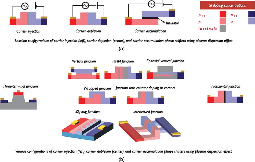
Carrier injection is the most efficient plasma dispersion-based modulation scheme.7,8,37,98 Most of the early demonstrations of high-speed modulators relied on carrier injection of minority carriers by forward biasing a PIN junction built along a waveguide.63,89,90,93,216,226 The carrier injection-based modulators provide a high modulation efficiency due to their large diffusion capacitance (typically ) when implemented on a waveguide with a small cross section with stronger confinement.7,37,65–67,91–94 Carrier injection-based modulators are reported using lateral PIN63,65,67,92 and vertical PIN configurations (see Fig. 1).63,89,93,216,226 Owing to the feasibility for a short phase shifter ( a few hundreds of ), carrier injection modulators typically use lumped driving schemes.7,65,67 The use of pre-emphasized electrical signaling schemes, in which a fraction of the electrical driver signal has a voltage of the modulator, boosts the limited speeds of carrier injection-based modulators67,95–97 with the obvious ramification of increased power consumption. Recent years have seen the development of passive equalization techniques to boost the high-speed operation of the carrier injection modulators.65,67 The studies have shown that the factors that limit the speed of the carrier injection-based modulation are (a) recombination time of the injected electron–hole pairs and (b) the sum of the electrical driver output resistance and the bulk resistance of the p- and n-doped regions.7,65,67 The slower of these two effects determines the speed limit of the carrier injection modulators.67 Practically, it is possible to improve the bandwidth of carrier injection modulators by embedding an passive equalizer such that and , where and are the equalizer and the forward resistance and the capacitance, respectively.7,65,91 Current state-of-the-art carrier injection modulators use this passive equalization to demonstrate operation.7,65 Recently, 70 Gbaud operation of a carrier injection MZM was enabled by passive RC equalization.7 The modulator has a 37-GHz 3-dB bandwidth using a 0.25-mm long-phase shifter having loss and a of .7 One of the best modulation efficiencies of has been reported in Ref. 67, where a side-wall corrugated MZM with a bandwidth of 12.5 GHz is operated at using a finite impulse response filter for frequency compensation necessary for the broadband operation.67 The demonstrated modulator had a -long phase shifter that exhibited a propagation loss of .

Figure 1.(a) Baseline architecture of carrier injection, carrier depletion, and carrier accumulation plasma dispersion phase shifters. (b) Various configurations of plasma dispersion phase shifters.
The carrier accumulation plasma dispersion phase shifter requires forward biasing of a metal-oxide-semiconductor (MOS) capacitor.2,68,101,102 A typical implementation of an MOS (also known as silicon–insulator–silicon capacitor—SISCAP) modulator comprises a vertical slot waveguide with an overlapping stack of a -sized thick p-type poly-silicon layer on top of a -sized thick n-type c-silicon layer with a few nm (typically ) thick insulating gate oxide layer in the middle (i.e., p-Si/insulator/c-Si vertical slot waveguide)—see Fig. 1(a).69,101,102 Under accumulation conditions, in which a positive bias is applied to the p-type layer, the vertically confined optical mode overlaps strongly with the highly capacitive gate section.101,102 This enables modulation efficiency for SISCAP modulators37 with state-of-the-art values as low as 0.2 and .5,68,69 Owing to this higher modulation efficiency, typically -long phase shifters with lumped electrical driving are implemented in SISCAP modulators.65,67,69,69,103 The higher capacitance, which leads to higher modulation efficiency, caps the modulation speed of SISCAP modulators.2,104 The modulation efficiency and speed can be traded-off in SISCAP modulators by adopting the capacitance to a value that can provide either an efficient modulator (i.e., high capacitance) with low or high-speed modulator (i.e., low capacitance) without any degradation of the loss parameter for the modulator (the increase or decrease in capacitance is independent of the doping level and is controlled by the thickness of gate oxide and the relative permitivity of the material used as the gate oxide).2,70,101,102,104 Typically, a vertical capacitor configuration is used in SISCAP modulators due to the ease of fabrication.5,68,69,69,70,104 It is straightforward to fabricate by the deposition of poly-Si.2,101 Techniques such as epitaxial lateral growth101,102 and laser-induced epitaxial growth crystallize the poly-silicon layer to overcome the higher scattering loss due to defects in the lattice.2,227 Recently, SISCAP modulators using a c-Si/insulator/c-Si in a vertical slot configuration70 and in a horizontal slot configuration103 without requiring any additional processing steps have been reported [see Fig. 1(b)]. One of the first Mach–Zehnder SISCAP modulators relied on a vertical capacitor configuration, and it delivered an ER of 9 dB.68 The design consisted of a -long MOS capacitor with a loss delivering a of 0.2 cm for the O-band. The same MZM is driven by a CMOS driver to demonstrate its low-power operation for NRZ-OOK and for advanced modulation formats such as PAM-4 using a segmented driver.5 A recent demonstration reports high modulation efficiency of for operation using a -long phase shifter with a loss of .69 The MZM provided one of the best FoMs () of . A microdisk-based SISCAP modulator demonstrated operation on a small footprint of consuming only .70 In order to deliver operation using SISCAP modulators, a parametric study has been performed validating the trade-off between high-speed operation, modulation efficiency, and loss.104
Depletion of electrons and holes by reversely biasing a PN junction built in or around it is the most widely adopted scheme to implement the plasma dispersion-based phase modulator.8–11,13–19,22,32,33,71,71–87,106–121 Depletion-based modulators were the first all-silicon modulator to reach speeds of 40106 and .16 The current highest reported data rates of using OOK modulation were also demonstrated in carrier depletion modulators.122,123 Carrier depletion phase shifters exhibit a relatively limited capacitance of 0.2 to 21,91 and, hence, a limited modulation efficiency. In order to improve the modulation efficiency, the capacitance can be increased by either shrinking the mode size (determined by the waveguide geometry) or by reducing the width of the depletion region (higher transition capacitance).21 The latter requires higher doping concentrations, which leads to higher loss due to free carrier absorption. Over the years, a wide variety of PN junction designs are reported to solve this challenge of optimizing modulator speed, efficiency, and loss at the same time.13,15,17,18,22,71–76,78,107–109,116,117,119 Distinct categories of PN junction implementation are as follows:
One of the first modulators relied on a vertical PIN junction and delivered a modulation efficiency of and phase shifter loss of .106 Using a vertical P(I)N junction design, an athermal microdisk modulator with a high modulation efficiency of consuming while operating at using NRZ-OOK signaling has been reported.18 At , the modulator had an IL of and an ER of 6 dB. One of the highest operating speeds of with 3.8 dB ER comprised a symmetric PN junction.17 In this case, the modulator operated in a series of push–pull modes by connecting back-to-back the phase shifter PN junction embedded on both arms of the MZI. The series connection of the two phase shifters halves the net capacitance, and the push–pull scheme limits the chirp of the modulator. The modulator shows 50 GHz bandwidth at 4 V reverse bias and an average modulation efficiency of for a 4-mm-long PN junction.17 In another implementation, a symmetric carrier depletion MZM with sub-1 V drive signal operated at and delivered a power consumption as low as .118 Yet another variant of the symmetric lateral PN junction used the doping compensating technique120 to demonstrate a MZM comprising a 3-mm-long phase shifter with a modulation efficiency of and a loss of 3.9 dB. An RM relying on a symmetric phase shifter configuration delivered a modulation efficiency of at 0 V119 to demonstrate energy consumption for operation on a compact footprint of . A recent implementation demonstrates a MZM, in which the carrier depletion-based phase shifter is implemented through a -long photonic crystal slow light structure.114 The modulator used a meandered RF electrode terminated with a resistor to provide a bandwidth of 38 GHz by preventing the velocity mismatch of the electrical and optical signals. The modulator required a voltage swing of 5.5 V to provide an energy consumption of and provided 4.8 dB ER. The literature also reports various other demonstrations of asymmetric (where there is an offset of the PN junction from the waveguide center) carrier depletion-based phase shifters.8,16,72,74,76 For example, a Michelson interferometer with a partially shifted PN-junction provided one of the highest modulation efficiencies of at 1 V reverse bias and 4.7 dB loss for a -long PN junction with a lumped driving scheme to operate at through a bandwidth extension scheme involving a resistor parallel to the PN junction.8 The asymmetric PN diodes are also exploited by RRs72,76 to demonstrate low-power (sub-) and compact depletion modulators. The literature also reports fully shifted PN junctions, where a self-aligning process allows for the alignment of the n-doped region to the edge of the waveguide.16,74 In one implementation of a fully shifted PN junction, a MZM modulator provided a modulation efficiency of and an IL of 4 dB for a 1-mm-long phase shifter.16 By further optimizing the implementation of self-aligned PN junctions,74 a demonstration provided an loss without compromising the speed of the modulator. The self-aligning process is further exploited to implement a PIPIN phase shifter with a modulation efficiency of for a 0.95-mm-long phase shifter introducing 4.5 dB optical loss when operated at .79 Depletion-based modulators relying on an interleaved phase shifter design have also delivered high-speed operation. A modulator comprising a 3-mm-long interleaved phase shifter reported a high modulation efficiency of with a static IL of 2.8 dB while delivering modulation speed.81 An RM comprising a ring resonator with a radius, and an MZM with a 0.95-mm phase shifter length operated at speed using an interleaved phase shifter delivering a modulation efficiency and loss of and , respectively.32 Apart from standalone implementations of high-speed phase shifters through these three baseline junction configurations and their adaptations, there are reports on junction implementations that rely on combining these three schemes in a single PN junction design.9,33,79,85,86 An example is the substrate-removed “zig-zag” phase shifter for an MZM delivering modulation efficiency for a 2-mm-long phase shifter with 4.4 dB loss.14 The modulator provided 55 GHz bandwidth and modulation speed of .14,87 Another example includes a phase shifter for operation of a racetrack RM by combining horizontal, vertical, and interleaved approaches. This implementation delivered a modulation efficiency of at reverse bias and a loss of .33 A recent result demonstrated an RM with a record low modulation efficiency of by employing a phase shifter comprising a combination of horizontal and vertical junctions by wrapping the n-doped region over the intrinsic and the p-doped region.9 The modulator showed 50 GHz bandwidth and delivered energy consumption for operation.
In the discussion presented above, we have provided a summary of the latest developments made for the improvement of plasma dispersion effect-based modulators. Figure 1(a) represents the three baseline plasma dispersion phase shifter architectures and their respective biasing configuration. Figure 1(b) gives an overview of a variety of other phase shifter configurations for carrier injection, carrier depletion, and carrier accumulation phase shifters.
Table 2 summarizes the typical performance for the injection, accumulation, and depletion-type plasma dispersion modulators. Table 2 also presents the best-reported results for the modulation efficiencies, losses, data rates, and energy consumption. There is an interplay of a vast pool of variables, such as junction type and its actuation mechanism, doping concentrations (typically ranging from to ) and their positions, the thickness of the slab waveguide (typically ranging from 1/3 to 1/4 of the guiding silicon thickness), the thickness of the guiding silicon layer (typically ), choice of the passive structure for the translation of phase modulation to amplitude modulation, and the design of the driving electrode (lumped, TW, and segmented), which can influence the performance of plasma dispersion modulators. In many cases, one performance parameter has to be delicately traded-off for another specification. This makes the design of a plasma dispersion modulator, which can meet all of the performance requirements concurrently, far from trivial. Operation of plasma dispersion modulators at speeds 7,14,122 consuming tens of fJ/bit with high modulation efficiency enabling micrometer-sized footprints has been accomplished. Recent developments have resulted in a co-designed SiPh modulator-driver offering while preserving a good modulation efficiency122 and without any customized fabrication process development. The plasma dispersion modulators deliver sufficient linearity and ER to handle advanced coherent modulation schemes,3,55,56,124–126 such as QAM, and amplitude modulation schemes,9,17,29,52,66,115,123 such as PAM. Furthermore, the plasma dispersion modulators have shown modest chirp-induced penalty for short- and long-haul links.3,26,30 The co-design and co-optimization of the driver–modulator design is the key to taking the performance of plasma dispersion modulators to a new level.122
| Principle | Modulation efficiency () | Loss (dB/cm) | Lengtha of phase shifter (mm) | Data rateb(Gb/s) | Energy/bit (fJ/bit) |
| Carrier injectionc | < (0.0588) | (287) | to < | < (707) | for MZMs and RMs (0.1f,98) |
| Carrier accumulationd | < (0.1669) | 50 to 80 (69) | | (405) | > for MZMs, < (3105) for SLMsg |
| Carrier depletione | (0.529) | 10 to 30 (2.610) | > | > (100122,123) | for MZMs (32.419), < for RMs (0.918) |
Table 2. Typical and state-of-the-art performance matrix for the plasma dispersion high-speed phase modulators. The parentheses contain the best-reported result for a performance attribute. The matrix includes the results reported for O-band and C-band demonstrations.
3 New Materials on Silicon for High-Speed Modulators
Recent years have seen growing efforts to integrate materials with strong electro-optic effects on SiPh platforms.153–192,192–208,228 The integration of new materials provides routes for optically broadband and energy-efficient high-speed modulation with little or no current flow.176,181,184,188,202 Furthermore, in some cases, these new materials provide an excellent decoupling between amplitude and phase modulation, which is difficult to achieve with contemporary all-silicon plasma dispersion modulation schemes.174,178,184
Through the wafer-scale integration of these new material systems with SiPh platforms, one can achieve impressive modulator performance, while at the same time preserving the benefits provided by the mature SiPh technology.181 These new materials can be broadly categorized into the following:
Early results of high-speed modulators by integrating electro-optic materials with the SiPh platforms have shown a lot of promise. Many research teams are attempting to take their maturity and performance beyond the performance of plasma dispersion modulators. The sections below discuss the key modulator implementations by integrating these materials into SiPh platforms.
3.1 (Silicon-)Germanium
The FK effect and the QCS effect provide possible routes to implement compact, low-power, and high-speed electro-absorption modulators (EAMs) in SiPh.31,143,144,146,149 Under the influence of an applied electric field, the band edge tilts to enhance the absorption coefficient for GeSi bulk material (FK effect) or Ge/SiGe quantum well (QW) structures (QCS effect).31,38,145,146 These effects are intrinsically fast through their sub-ps response time.34,229 The QCS effect is stronger than the FK effect134,230 due to the strong excitonic effect and discretized density of states. The integration of bulk GeSi or Ge/SiGe QW requires epitaxial growth on SiPh platforms. The FK effect is considered more attractive than the QCS effect in the context of integration feasibility. The latter requires a more complex epitaxial growth process for band alignment and strain balancing.152,230 A large change in the absorption coefficient (typically ranging from 100 to in the C-band146) enables the implementation of a compact and energy-efficient EAM using the FK effect and QCS effect.31,230 Both effects rely on band engineering. Therefore, they have limited optical bandwidth ( for the FK effect and for the QCS effect).134,149 In one of the first SiPh EAMs, the L-band absorption spectrum is shifted to the C-band by a tensiled 0.8% GeSi alloy.31 On a small footprint of only , the EAM actuated by a vertical PIN diode provided an energy consumption of only . This EAM could operate over a 14-nm bandwidth from 1539 to 1553 nm and delivered an efficiency (defined as , where is the absorption difference between ON-state and OFF-state, and is the absorption for the ON-sate, in which no electric field is applied) of 2. Despite the limited bandwidth of 1 GHz, this promising demonstration triggered other demonstrations of EAMs.20,38,128,133–139,231,232 An evanescently coupled GeSi EAM has been reported on a thick SOI platform (silicon guiding layer thickness of ), actuated by a horizontal PIN junction.135 This EAM is butt-coupled to the thick SOI waveguide through an appropriately designed taper.135 The modulator has an efficiency of . This EAM operated in the C-band and provided operation with energy consumption.135 Literature also reports an L-band Ge EAM and a GeSi C-band EAM with an electrical 3-dB bandwidth of for an optical bandwidth of 30 nm.136 In this case, the EAM is butt-coupled to a silicon waveguide through a tapered waveguide section. The Ge or GeSi alloy, which is grown on a silicon recess, has a lateral PIN diode. A highly doped contact on the silicon layer biases the EAM. The modulator consumed energy at modulation speeds of and provided an FoM of . Using this GeSi EAM, a digital to analog converter-less and digital signal processing (DSP)-free transmission over a 500-m-long single-mode fiber using NRZ-OOK signaling has been reported.20,137
There are various reports on the implementation of the Ge/SiGe QCS effect-based modulators.141–152 In one case, a Ge/SiGe QW modulator is butt-coupled to a thin SOI rib waveguide in such a way that the QWs and the rib waveguide are vertically aligned with each other to have maximum overlap.147 The active section of the modulator, which comprised 15 pairs of QWs, is driven by a vertical PIN diode. The modulator showed 3.5 GHz bandwidth by using a 1-V voltage swing (5.5 to 6.5 V) to provide of ER. In another implementation, Ge QWs are epitaxially grown at temperatures below 450°C on the silicon-rich low-loss waveguide platform.141 The concentration is selected such that it simultaneously ensures low indirect bandgap absorption and a sufficiently small lattice mismatch with the QWs. The modulator with 6.3 GHz bandwidth and 0 to 3 V swing provided ER and 3 dB IL.
The FK effect or QCS effect electro-absorption amplitude modulators allow for the implementation of coherent 231,232 and advanced amplitude modulation schemes such as PAM-4.233 These modulation schemes are a promising solution for short- and long-reach links because they are spectrally efficient while being tolerant of optical fiber transmission impairments.54,55,231 The implementation of an EAM-based or PAM-4 modulators relies on balanced MZIs with an EAM and a fixed phase-shift in the arms of the MZI.231–233 Typically, an unequal splitting of the optical carrier is required by the splitter of the MZI to achieve the appropriate eye-opening for PAM-4 or constellation for the signal.233 Literature reports an EAM-based PAM-4 modulator by integrating an EAM in each arm of a two-port balanced MZI.231–233 In this modulator, a fixed phase shift is provided by embedding a thermal phase shifter in one of the two arms of the MZI. The device modulated a PAM-4 signal without requiring any DSP. Furthermore, there are reports on the demonstrations of modulating QPSK and 16-QAM signals using EAM-based coherent modulators.231,232 The energy consumption of these modulators takes a hit due to the power-hungry thermo-optic effect required to provide a fixed phase shift in the arms of the MZIs.
Figure 2 represents the typical cross sections of FK EAMs and QCS effect-based EAMs in SiPh. This figure also summarizes the integration routes of these materials with SiPh. Table 3 summarizes the typical and the best-reported performance for the (silicon-)germanium modulators. This table covers the performance of the FK effect-based EAMs as well as QCS effect-based EAMs. The FoM for both FK and QCS effect-based EAMs is typically , although QCS effect-based modulators can potentially deliver better FoM due to their stronger excitonic absorption peaks.144,149,152 In most cases, FK-effect-based EAMs operate either in the L-band or C-band.150,152 It is possible to tune the operating wavelength of the QCS effect modulators by a bias voltage.150,152 Therefore, the QCS effect modulators can operate in the O-band as well. In terms of high-speed operation, FK effect-based EAMs have reached line rates of up to for OOK modulation schemes,137 whereas the QCS effect-based modulators have not yet demonstrated such a high speed of operation.
Figure 2.Representative cross sections of (a) FK-based EAMs and (b) QCS effect-based EAMs in SiPh. This figure also highlights the integration route for the respective EAMs. The term monolithic refers to the integration of a material with an SOI substrate using wafer-scale epitaxial growth resulting in PICs made out of one substrate technology in mass on a wafer level.
| Principle | FoM ER/IL | Loss (dB) | Modulator length (mm) | Data ratea (Gb/s) | Energy/bit (fJ/bit) |
| FK effectb | < (231) | < (4.8133) | | > (100137) | < (1320) |
| Quantum-confined Stark effectc | < (7.9149) | < (1.3149) | < | < (7147) | < (16148) |
Table 3. Typical and state-of-the-art performance matrix for amplitude modulation by the FK effect and QCS effect. The best-reported performance attributes are mentioned in parentheses.
3.2 Ferroelectrics
Ferroelectrics are materials possessing spontaneous polarization that can be altered by the application of a sufficiently strong electric field.234 As ferroelectric materials are non-centrosymmetric, they exhibit a Pockels effect.234 Many ferroelectrics have large Pockels coefficients compared to non-ferroelectric inorganic materials. The dominant contribution to the Pockels coefficients in these ferroelectrics tends to come from lattice vibrations rather than electron movements.234,235 Because of their strong Pockels effect, the integration of ferroelectric materials such as ,167–174 barium titanate (),175–182 and lead zirconate titanate (PZT)183–185 with SiPh provides a promising route for the implementation of efficient, high-speed modulators.2,175,228 A variety of integration techniques have been explored, such as molecular beam epitaxy (MBE),176,178 pulsed laser deposition,236,237 chemical solution deposition (CSD),238 RF magnetron sputtering,239 metal organic chemical vapor deposition,240 and atomic layer deposition.241 The two key requirements for integrating ferroelectric materials with SiPh are to ensure a high electro-optic coefficient and low propagation loss.182 The following sections will review the latest developments to implement high-speed modulators by integrating ferroelectric materials with SiPh.
3.2.1 LiNbO3 on silicon (nitride) high-speed modulators
is a widely used material for modulators and provides high-speed devices with a bandwidth of .27,242,243 modulators have been used for a long time in fiber-optic networks.242,244 These devices are based on low-index-contrast waveguides in bulk ,242 in which the index contrast between the core and cladding of a waveguide is provided by the diffusion of Ti or Li ions.242 The weak optical guiding resulting from the low-index-contrast requires the electrical contacts to be placed far away from the waveguides, resulting in typical of 10 to .242 Recent demonstrations of high-index-contrast -on-insulator (LNOI) modulators have shown energy-efficient operation (a few tens of fJ/bit energy consumption) with 100-GHz bandwidth, modulation efficiency, and loss for a device that is a few millimeters long (typically 2 to 20 mm long).243,245–247 These thin-film LNOI modulators rely on layers of a few hundred nanometers thickness, which are bonded on top of .243 Several approaches have been reported in the last two decades to integrate with silicon at room temperature245,248,249 and to demonstrate high-speed modulation by bonding with silicon167–169,250 or silicon nitride.170–172 The Pockels coefficient of integrated is comparable to that of bulk ,249 but most of these integration attempts have resulted in modulator bandwidths that are smaller than the all-silicon modulator implementations.173 Recently, a tremendous boost in the speeds (not yet the overall performance) of such modulators has been reported.173,174 For example, for a 5-mm long TW-MZM that was realized by direct oxide bonding of thin-film on top of a silicon waveguide, a bandwidth of 100 GHz and a loss of 7.6 dB have been reported.173 The modulator had a limited efficiency of due to vertical coupling of light into the unpatterned membrane on top of the silicon waveguide. In another implementation, the complete coupling of light from a silicon waveguide to a patterned rib waveguide through a vertical adiabatic coupler resulted in a modulation efficiency of .174 With a 2.5-dB loss, the 5-mm-long phase shifter embedded in an MZI and driven by a TW electrode in the push–pull configuration provided 70 GHz bandwidth and enabled single-lane NRZ-OOK transmission. Unlike the other reported implementation,173 the integration of with the SiPh PIC was carried out using BCB-bonding. Monolithic integration of with SiPh PICs has yet to be reported.
3.2.2 BaTiO3 on silicon high-speed modulators
In recent years, there has been a lot of interest in the integration of with SiPh.175–182 is a promising material for integration with SiPh because of (a) its high Pockels coefficient [in bulk form, has a Pockels coefficient of ,27,175,249 whereas BTO offers one of the highest Pockels coefficients () in bulk form176,251]; (b) feasibility of integration with a silicon substrate;252 (c) capability to offer high-speed modulation;253 (d) high chemical and thermal stability of BTO; and (e) feasibility of low-loss hybrid BTO-Si passive circuitry.178,179 The integration of BTO with SiPh relies on epitaxial growth enabling integration compatible with 200 and 300 mm silicon wafers.181 The large lattice mismatch () between BTO and Si makes the integration of the two materials far from trivial.254 A (STO) buffer layer of a couple of nanometers thickness reduces this lattice mismatch to .228 Among the various possible routes to grow BTO on SiPh platforms, MBE is known to provide the highest () Pockels coefficient in BTO thin films.176 In one approach, the BTO growth is done directly on an SOI wafer.177 Afterward, an amorphous silicon layer with a thickness equal to the thickness of the c-Si layer of the SOI wafer is grown. The resulting heterostructure is patterned lithographically to form a horizontal slot waveguide. Stronger guiding of the optical signal in the low-index BTO layer () enhances the overlap of the optical and electrical field in the BTO layer. This approach provided a Pockels coefficient of .177 A ring-based modulator with a modulation efficiency of and a bandwidth of 4.9 GHz has been reported, where the limited bandwidth is associated with the parasitic electrical effects.177 A key challenge faced by the integration approach mentioned in Ref. 177 and other integration approaches176,178 is the high propagation loss ().176–178,255 The origin of this high loss is attributed to the absorption of hydrogen by the STO seed layer during the fabrication of the slot waveguide.178 Furthermore, it has been shown that a loss of in a strip-loaded horizontal slot waveguide can be achieved by low-temperature annealing.178 Apart from the aforementioned approach, where BTO is grown directly on an SOI wafer,177 another possible approach entails the formation of a BTO/Si heterostructure by bonding an SOI wafer with a BTO layer grown on a host SOI wafer.176,179 For such a bonded BTO/Si heterostructure, a Pockels coefficient of has been reported (30 times larger than that of a structure).179 In one implementation, a plasmonic MZM with a -long BTO/Si phase shifter with 25 dB loss delivered and required a of 14.5 V (modulation efficiency of ).180 The modulator operated successfully for temperatures up to 130°C. Furthermore, a wafer-level bonding of Si/BTO heterostructures on the back-end-of-line (BEOL) dielectric layer of an advanced SiPh platform has been reported.181 This integration led to the demonstration of an MZM with a limited bandwidth of 2 GHz (mostly limited by the electrical bandwidth of the electrodes).181 The modulator had a modulation efficiency of and loss of for a 1-mm-long phase shifter.181,182
3.2.3 PZT on silicon nitride high-speed modulators
PZT is an orthorhombic lead-containing ceramic ferroelectric material.256,257 Though BTO has a large Pockels coefficient, its use in SiPh requires complex and expensive integration technology.178,181,182,255 As compared to BTO, PZT has a smaller Pockels coefficient, but it can be deposited by a low-cost and simple CSD method.185,257 Ultra-thin lanthanide-based intermediate seed layers enable the deposition of high-quality thin (up to 200 nm) PZT layers on silicon,257 with Pockels coefficients up to .228 PZT thin films have been integrated with silicon nitride photonic circuits. An RM with a bandwidth of 33 GHz and an MZM with a bandwidth of 27 GHz have been demonstrated,184 with a modulation efficiency of and a loss of . The PZT layer was deposited on a planarized silicon nitride PIC (i.e., the PIC consisted of silicon nitride strip waveguides with oxide bottom and side cladding, while the top cladding was air). The PZT thin film was poled by applying a voltage of 60 to 80 V for 1 h.185
Figure 3 represents the typical cross sections of ferroelectric modulators in SiPh. This figure also summarizes the integration routes of the respective materials with SiPh. Table 4 presents a summary of the typical and the best-reported modulation efficiencies, losses, data rates, and energy consumption for the ferroelectric-based modulators in SiPh. For all three types (i.e., , BTO, and PZT), modulation speeds have been demonstrated. -based modulators are outstanding in terms of low-loss operation and have delivered speeds of . In terms of modulation efficiency, BTO-based modulators have shown a lot of promise with typical reported values of .
Figure 3.Representative cross sections of (a) , (b) BTO, (c) PZT, and (d) organics modulators in SiPh. This figure also highlights the integration route for each material. The term monolithic refers to the integration of a material with a SiPh substrate using wafer-scale epitaxial growth resulting in PICs made out of one substrate technology in mass on a wafer level.
| Scheme | Modulation efficiency () | Loss (dB/cm) | Length of phase shifter (mm) | Data rateb(Gb/s) | Energy/bit (fJ/bit) |
| integrated with SiPhc | < (2.2174) | (0.98174) | > | > (100174) | > (170174) |
| integrated with SiPhd | < (0.2182) | > (6182) | > | > (72180) | <179 |
| PZT integrated with SiPhe | 1 (1183) | 1 (1183) | > | 40 (40184) | - |
| Organics integrated with SiPhf | < (0.032190) | < (20228) | < | > (100196) | < (0.7192) |
Table 4. Typical and state-of-the-art performance matrix for the ferroelectric and organic high-speed phase modulators in SiPh.a The parentheses contain the best-reported result for a performance attribute.
3.3 Organic Electro-Optic Materials
Organic electro-optic materials are typically based on -conjugated molecules with strong electron donor and acceptor groups at the ends of the -conjugated structure.188,258 The delocalized electrons associated with this -conjugated structure are confined by a strongly asymmetric potential well, giving rise to large Pockels coefficients.188,258 In contrast to the ferroelectrics discussed above, the Pockels effect in these organic electro-optic materials is mostly electronic in nature and can thus provide an ultra-fast response.188,190,228,258 Organic electro-optic materials can be processed at room temperature using inexpensive solution-based techniques, whereas the growth of inorganic Pockels materials typically requires high temperatures and/or the use of vacuum equipment.177,182,188,255,258
A combination of organic materials with SiPh devices has resulted in the so-called silicon-organic hybrid (SOH) class of modulators.186–188,197 The underlying organic materials in SOH modulators are designed to provide high electro-optic activity with experimentally demonstrated values of .190 This results in modulators with a low-loss,194 a low-chirp parameter of ,193 and a high modulation efficiency (),190 along with a high modulation bandwidth ()191,259 and low-energy consumption of a few fJ/bit.192,228 With -voltages below 1 V, SOH modulators may be directly driven by standard CMOS circuits without the need for any additional drive amplifiers,260 thereby opening a path toward greatly reduced power dissipation in highly integrated transceivers. For the fabrication of SOH devices, the organic electro-optic material is deposited onto fully processed SiPh chips in a postprocessing step, which requires removal of the BEOL layer stack of a standard SiPh process flow.228 SOH modulators rely on slot waveguides,188,191 which guarantees enhanced interaction between the highly confined optical mode in the slot waveguide and the organic electro-optic material filling the slot. To pole the electro-optic material after deposition, the devices are heated, and a DC voltage is applied across the slot waveguides. This non-volatile poling transforms the random orientation of the electro-optic chromophores in the slot into an acentric orientation, thereby leading to a non-zero Pockels coefficient. After cooling down the device to ambient temperature, the voltage can be removed, and the poled electro-optic material preserves its orientation. SOH modulators have shown exemplary performance over the years. Some key results are reported in Refs. 189–191, 193, 196, and 261. The main skepticism faced by the SOH modulators comes from their long-term photochemical and photothermal stability. Recent research results reported in Refs. 195 and 262 have shown long-term stability of SOH devices following Telecordia standards. These early experiments have shown that in storing the SOH modulators at elevated temperatures of 85°C, the degradation of the electro-optic activity converges to a stable level where the -product increases by after 2400 h.
The limitations of poled organic materials can be overcome by substituting them with crystalline organic materials, which are inherently resilient to higher temperatures with good photochemical stability and do not require any poling.199 The electro-optic coefficients of the organic crystals are smaller (typically )263 than those of the poled organic polymers.190 The integration of organic crystals requires growth to functionalize the silicon waveguides.198,199 An N-benzyl-2-methyl-4-nitroaniline crystal has been deposited on an SOI waveguide to demonstrate an MZM that could operate at with a modulation efficiency of and a loss of 16 dB in the phase modulator with a 1.5 mm length.199
Typically, the analogue bandwidth of current SOH modulators is limited to by the finite conductivity of the doped silicon slabs that provide an electrical contact with the rails of the slot waveguide.190 These bandwidths may be improved to more than 100 GHz by exploiting optimized waveguide designs that rely on multi-step doping profiles.259 To that end, doped silicon slabs have also been replaced by BTO to feed the modulating RF signal to the EO material in the slot waveguide.200 This so-called capacitively coupled SOH MZM delivered a bandwidth of 65 GHz, which was sufficient to produce a OOK signal.200 The modulator had a modulation efficiency of ; the loss from the phase shifter section is not reported. Yet another variant of the SOH modulator is the plasmonic-organic hybrid (POH) modulator,258,264–269 where the silicon slot waveguide is replaced by a metal plasmonic slot waveguide to provide even higher optical confinement.258,265 The deposition of an organic electro-optic material on the metal slot waveguide leads to compact high-speed devices with bandwidths of hundreds of gigahertz.266,270 POH modulators are compact with typical lengths of a few microns and offer a low-energy consumption of a few tens of fJ/bit along with ultra-low voltage-length products of typically 258—nearly an order of magnitude lower than those of classical SOH modulators. The obvious limitation of the POH modulators is the high propagation loss in the plasmonic slot-waveguide section with typical values of .200,258 Despite the high efficiencies, this leads to substantial -voltage-loss-products of the order of .188
Table 4 provides a summary of typical modulation efficiencies, losses, speeds, and energy consumption for organic electro-optic modulators in SiPh. When compared with the other Pockels modulators, the organic electro-optic modulators provide the best modulation efficiency with a reported value of .190 Organic electro-optic modulators have shown up to 196 operation and sub-fJ/bit energy consumption.192Figure 3(d) represents the typical cross section of organics modulators in SiPh.
3.4 III–V Semiconductors
The integration of III–V semiconductors with SiPh platforms is a well-established research field, as it provides a viable route for the integration of laser sources with SiPh PICs.271–275 Direct bonding,272 BCB-aided adhesive bonding,271 III–V/Si flip-chip bonding,275 and transfer printing274 are some of the most established bonding mechanisms for III–V/Si integration. Demonstrations of III–V integration with advanced SiPh platforms have been reported.276,277 Demonstrations of epitaxial growth of III–V on Si have also been reported despite the large lattice mismatch between Si and III–V (for example, InP has 8% lattice mismatch with Si).278,279 The integration of III–V on silicon also provides a route for the implementation of efficient high-speed modulators because they provide (a) a large electron-induced refractive-index change, (b) a high electron mobility, and (c) a low carrier-plasma absorption.166
The reported implementations of III–V/Si modulators typically use a MOS (SISCAP) modulator architecture.161–163 In these modulators, n-doped III–V material, for example, InGaAsP, is bonded to a p-doped Si layer with an insulating layer separating the two.161–163 This results in a SISCAP architecture, where the insulating layer acts as a capacitor. A change in the refractive index takes place due to the charge accumulation due to the biasing of the doped silicon and III–V layer. According to Drude’s model, the plasma dispersion induced refractive index change is inversely proportional to the effective masses of the electrons and holes.61,89 As compared to the electron mass of Si, the lighter electron mass of n-doped III–V results in a 17 times stronger electron-induced refractive index change.161 Furthermore, an n-doped III–V provides a larger ratio of to , where is the change in the absorption coefficient,161 resulting in a phase modulator with reduced spurious intensity modulation (“pure-phase” modulation). Similarly, p-doped silicon provides larger than p-doped III–Vs for carrier concentrations below .161–163 Therefore, a hybrid III–V/Si MOS modulator brings the best of III–V and Si together. Consequently, this approach offers modulators with a 3 to 5 times better modulation efficiency compared to all-silicon MOS modulators and a phase shifter loss that is significantly lower than in all-silicon MOS modulators.161,163
In one report, an MOS structure provided a modulation efficiency of and a phase shifter loss of .161 In another report, an MOS structure provided163 a modulation efficiency of with an absorption loss of in the phase shifter. Both demonstrations show an impressive modulation efficiency. But, the electro-optic cut-off frequency is rather limited due to the large oxide capacitance in the carrier accumulation mode of operation.161,163
One possible approach to break the trade-off between the high-speed operation and high modulation efficiency banks on operating the III–V on Si MOS phase shifter in reverse bias.165,280 The III–V on Si MOS modulator that is operated in reverse bias is architecturally similar to the forward biased III–V on Si modulator.161,163,165,280 For a given thickness of the oxide layer, the reverse biased III–V on Si phase shifter has a reduced depletion capacitance as compared to the accumulation capacitance.165,280 The combined plasma dispersion effect and FK effect in the reverse biased III–V on Si MOS phase shifter ensure a modulation efficiency that is comparable to that in the accumulation mode while ensuring a low-loss operation due to the limited hole density in the n-doped InGaAsP layer of the modulator.165,280 A III–V on Si MOS modulator with a -long phase shifter and a 9-nm-thick oxide layer has been reported with a modulation efficiency of .165 As compared to the carrier accumulation MOS, the reverse biased MOS provides a lower depletion capacitance, hence paving the way for a improvement in modulation bandwidth and energy consumption per bit. The implementation of III–V on Si MOS modulators is not limited to MZIs only.164 By implementing a III–V on Si MOS modulator in a racetrack configuration (implementing III–V on Si MOS modulators in a ring is challenging due to the long taper length needed for the III–V on Si hybrid waveguide), the energy consumption of a 40-GHz (3-dB bandwidth) modulator has been improved by a factor of 3.7 as compared to the III–V on Si MZMs, while delivering a modulation efficiency of .164 The -long phase shifter section of the modulators comprised a thin aluminum oxide gate layer separating the n-type III–V and the p-doped Si layer. Recently, a proof-of-concept, taper-less integration of a few tens of nanometers thick III–V layer with Si has been demonstrated to reduce the footprint and loss of the device281 without compromising the modulation efficiency of the III–V on Si MOS capacitor.
Apart from phase modulators, EAMs have been reported by the bonding of III–V QWs with silicon.140,282 These EAMs use a PIN architecture, where the application of a bias voltage changes the optical absorption of the intrinsic multiple QWs due to the QCS effect.282 A segmented electrode, comprising a low-impedance active modulation section cascaded by a high-impedance passive section, provides high-bandwidth operation while ensuring low reflection and good modulation efficiency.140 A bandwidth hybrid III–V on silicon EAM has been demonstrated using this scheme.140 In the O-band, this modulator has an IL of 4.9 dB, and it shows of dynamic ER for operation over a 16-km-long optical fiber link.
Figure 4 represents the typical cross sections of III–V on Si phase modulators and EAMs. This figure also summarizes the routes to integrate III–V on Si. Table 5 presents a summary of the typical and best-reported values for the modulation efficiencies, losses, data rates, and energy consumption for forward and reverse biased III–V on Si phase modulators as well as for III–V on Si EAMs. III–V on Si modulators have shown an impressive modulation efficiency and low-loss operation, but so far experimental demonstrations of high-speed operation () remain elusive.
Figure 4.Representative cross sections of (a) III–V on Si phase modulator and (b) III–V on Si EAM.
| Operation | Modulation efficiency () | Loss (dB/cm) | Length of phase shifter (mm) | Data ratea(Gb/s) | Energy/bit (fJ/bit) |
| Forward biased III–V on Si as a phase modulatord | < (0.047161) | < (19.4161) | < | > (32163,b) | |
| Reverse biased III–V on Si as a phase modulatord | < (0.11164) | (28280) | < | 200c,280 | 280 |
| Operation | FoM ER/IL | Loss (dB) | Modulator length (mm) | Data ratea (Gb/s) | Energy/bit (fJ/bit) |
| III–V on Si as an amplitude modulatord | (2140) | (4.9140) | | (50)140 | - |
Table 5. Typical and state-of-the-art performance matrix for the III–V on Si high-speed modulators in SiPh. The parentheses contain the best-reported result for a performance attribute.
3.5 2D Materials
Atomically thick 2D materials, the most prominent graphene, have received considerable interest in the last decade to implement efficient modulators by integration with Si/SiN PICs.1,153–160,201–208 The implementation of graphene-based modulators in SiPh involves the transfer of the graphene layer on a Si or SiN waveguide.1 Mature and wafer-scale chemical vapor deposition is the widely adopted scheme to deposit graphene on a variety of metallic and dielectric substrates.283–285 The transfer of the graphene layer on a Si or SiN waveguide is performed after delaminating graphene from the substrate while adding a polymer carrier to handle the graphene film.154,159 Recently, microtransfer printing technology has shown promising results to transfer graphene to the target substrate in an automatic fashion.159 A single graphene layer, which is only a fraction of a nanometer thick, can absorb 2.3% of light286 with a wavelength ranging from the visible to THz wavelengths (graphene is a gapless material). Furthermore, graphene has a very high electron mobility of (silicon has a carrier mobility of ).228,287,288 These two properties enable the implementation of high-speed electro-absorptive153 or electro-refractive201 modulators through the integration of graphene with SiPh ICs.
The two prominent types of graphene modulators in SiPh comprise a SiPh rib waveguide, which is either loaded with a single layer or a double layer of graphene153,156 (see Fig. 5). The operating principle of these modulators relies on the charging and discharging of a capacitor. A single-layer graphene modulator comprises a graphene loaded Si rib waveguide with a doped slab region.153 A few nm thick dielectric spacer, such as , , or hBN, separates the waveguide and the graphene layer to form a capacitor.1 The first reported graphene modulator153 had a 4-dB ER and relied on a single-layer approach. The EAM provided 1 GHz operation, limited by the RC time constant, and an electroabsorption modulation of .153 The absorption in graphene is dependent on the bias voltage.1 This voltage tunes the Fermi level of graphene to enable or inhibit the interband transitions by excitation of electrons through the incident photons.201,289 This change in absorption due to carrier accumulation in the graphene sheet results in modulation of light propagating in the waveguide. The doped Si waveguide in the single-layer graphene modulator is a source of loss, and it requires an implantation step.153,156 Double-layer graphene modulators remedy these limitations.156 They are separated by a dielectric layer that resides on top of a completely passive waveguide. (This architecture does not require any doping of the waveguide slab.)156 The first double-layer graphene modulator reported 1 GHz bandwidth and an electroabsorption modulation of .156 The -long modulator provided a 6-dB ER and required a 5-V driving voltage. One of the first multi-Gb/s graphene-silicon modulators157 relied on a single-layer graphene architecture that provided a 5.2-dB ER for a -long EAM operating at . At , the modulator provided a modulation efficiency of . The ON state loss is 3.8 dB with a power consumption of about . Another result reports a double-layer graphene RM158 using a critical coupling effect in a SiN ring. In this implementation, a 50-nm thick layer separates the two graphene layers. By biasing, the change in the transparency of the graphene capacitor led to the modulation of the optical signal. The reduced capacitance resulting from the thick spacer between the graphene layers led to a modulator showing 30 GHz bandwidth with a modulation efficiency of but required a DC bias and .158 The modulator could transmit while consuming . A positive chirp of a graphene EAM is an interesting property.160 This feature is useful in compensating for the chromatic dispersion in an optical transmission link for the transmission of without any optical signal to noise ratio penalty.160
Figure 5.Representative cross sections of (a) single-layer graphene phase/amplitude modulator and (b) double-layer graphene amplitude/phase modulator in SiPh.
Apart from amplitude modulation, it is also feasible to use graphene for phase modulation.201–208 Phase modulation is more exciting for the encoding of complex modulation formats such as QPSK. A single-layer graphene architecture, in which the graphene layer is separated from the silicon waveguide by a thin dielectric spacer layer, acts as a phase modulator by shifting the Fermi level of graphene.201,205,207,290,291 A single-layer graphene phase modulator of length is integrated on a Si MZI and showed a modulation efficiency of . The modulator delivered an ER of 35 dB, an EO bandwidth of 5 GHz, and a loss of .201 With a drive, the transmission of over a 50-km fiber span is demonstrated. The higher loss in the modulator is associated with the suboptimal transfer of graphene.201 The quality of graphene, which is typically determined by the scattering time and is related to the carrier mobility, plays a detrimental role in the performance of graphene modulators.1 Typically, scattering time of is required to implement energy-efficient graphene modulators with a high ER.1 Achieving graphene carrier mobility, which roughly corresponds to 300 fs scattering time, upon the complete modulator integration process would be ideal. Accomplishing this would lead to extremely low IL.289 In perspective, the combination of low IL in a dual-layer graphene structure, the high graphene electro-absorption, or electro-refractive efficiency would lead to a modulator with a good FoM.1 It is important to mention that graphene can be used for detection,1 and this makes graphene suitable for a telecommunication platform on a passive integrated circuit operating in several telecommunications bands.
Inspired by the promising results shown by graphene, other 2D materials such as tungsten disulfide () and molybdenum disulfide () have also been integrated with SiPh. Results show phase change relative to the change in absorption for these materials at telecom wavelengths when integrated with SiN.204
Figure 5 represents typical cross sections of a single layer graphene modulator (a) and a double layer graphene modulator (b) in SiPh. Table 6 provides the current state of high-speed phase and amplitude modulators in SiPh by integrating 2D materials. The currently reported performances of 2D modulators, in particular graphene modulators, are mostly limited by technological immaturity and not by conceptual limits. Graphene requires more development to reach the best performances. More specifically, graphene needs to preserve the high carrier mobility after the integration in the photonic circuit. This preservation is not the case yet. By achieving a high level of technological maturity, graphene has the potential to provide devices that can work over a wide range of wavelengths due to its gapless band structure, miniaturized devices due to its large EO efficiency, feasibility for BEOL integration with the SiPh fabrication process, and a possibility to offer a complete platform for communication applications, as graphene possesses properties for efficient modulation and detection.
| Operation | Modulation efficiency () | Loss (dB/cm) | Length of phase shifter (mm) | Data ratea(Gb/s) | Energy/bit (fJ/bit) |
| 2D Materials on Si as phase modulatorb | < (0.28201) | > (236201) | <d | (10201) | (600)1) for MZM; < for RM |
| Operation | FoM ER/IL | Loss (dB) | Modulator Length (mm) | Data ratea (Gb/s) | Energy/bit (fJ/bit) |
| 2D Materials on Si as amplitude modulatorc | < (4.9155) | < (0.9203) | < | > (50154) | (40202) |
Table 6. Typical and state-of-the-art performance matrix for graphene on Si high-speed modulators in SiPh. The parentheses contain the best-reported result for a performance attribute.
4 Summary and Outlook
Years of academic and industrial R&D have enabled a tremendous boost in the performance of plasma dispersion phase modulators. Operation at speeds of with high modulation efficiency is now feasible. Plasma dispersion modulators can operate with a sub-1-V drive signal consuming a few tens of fJ/bit in a -sized footprint. Demonstrations of advanced modulation schemes such as PAM-4, PAM-8, QPSK, 16-QAM, and 32-QAM have been reported in plasma dispersion modulators. The modulators have an insignificant chirp-induced penalty for long- and short-haul links. A closer synergy through co-design and co-optimization of electronic–photonic modulator design is the key to take plasma dispersion modulators beyond operation in an efficient manner. The last five years have seen a new paradigm in achieving higher speed and lower loss operations of SiPh modulators by integrating materials such as ferroelectrics, organics, SiGe alloys, III–Vs, and 2D materials. Unlike plasma dispersion modulators, which are commercially deployed and have a high manufacturing readiness level (MRL) of , these new modulators are still in the early R&D stage (MRL ) and are currently not included in any commercial product.
Electro-absorption modulation by (silicon-)germanium FK or QCS devices allows for micrometer-sized footprints. FK-EA modulation provides operation, but these modulators have a limited ER as well as limited operating optical bandwidth. QCS-EA modulation has integration challenges with SiPh. Moreover, their operating speed is . , , PZT, graphene, and organic thin films on Si PICs offer high Pockels coefficients, paving the way for linear and chirp-free high-performance SiPh modulators. Early results reported in the literature indicate that promising performance is achievable by integrating thin-film , , or PZT materials on Si. The integration of organic materials on Si has also shown operation and impressive modulation efficiency. Progress has been reported to address the lifetime issues, but more development is necessary before the commercial launch of high-speed modulators relying on organic electro-optic materials. Bringing together III–V and Si brings the best out of III–V and Si to implement MOS-type phase modulators and EAMs. The product of and phase shifter loss is impressive for the III–V on Si phase modulators, but high-speed operation remains elusive. (Theoretically, they have shown impressive results.) Integrating 2D materials, in particular graphene, with SiPh has the potential to provide a complete solution for modulation and detection at high speed. Multi-Gb/s operation has been reported for the graphene phase and amplitude modulators. A technique to preserve the high carrier mobility after integration in the photonic circuit is essential to unleash the true potential of graphene modulators in SiPh.
To conclude, modulator schemes that rely on the integration of efficient electro-optic materials with SiPh are gaining rapid technological maturity. They provide an additional route to fulfill the compelling needs of bandwidth, loss, and linearity at low-power consumption and cost for future high-speed optical links. It is important to note that the modulators based on the integration of efficient electro-optic materials with SiPh will not necessarily cannibalize or replace the plasma dispersion modulators. It is a way to overcome bandwidth and loss limits that stem from the physics of the plasma dispersion effect. However they will come at the cost of a more complex fabrication process. For this reason, the optimized solution will depend on the application.
References
[1] M. Romagnoli et al. Graphene-based integrated photonics for next-generation datacom and telecom. Nat. Rev. Mater., 3, 392-414(2018).
[2] J. Witzens. High-speed silicon photonics modulators. Proc. IEEE, 106, 2158-2182(2018).
[3] B. Milivojevic et al. 112 Gb/s DP-QPSK transmission over 2427-km SSMF using small-size silicon photonic IQ modulator and low-power CMOS driver(2013).
[4] S. S. Azadeh et al. Low Vπ silicon photonics modulators with highly linear epitaxially grown phase shifters. Opt. Express, 23, 23526-23550(2015). https://doi.org/10.1364/OE.23.023526
[5] M. Webster et al. Low-power MOS-capacitor based silicon photonic modulators and CMOS drivers(2015).
[6] A. Narasimha et al. A 40-Gb/s QSFP optoelectronic transceiver in a 0.13-μm CMOS silicon-on-insulator technology, OMK7(2008). https://doi.org/10.1109/OFC.2008.4528356
[7] Y. Sobu et al. 70 Gbaud operation of all-silicon Mach–Zehnder modulator based on forward-biased PIN diodes and passive equalizer, MD2-2(2019).
[8] D. Patel et al. High-speed compact silicon photonic Michelson interferometric modulator. Opt. Express, 22, 26788-26802(2014).
[9] J. Sun et al. A 128 Gb/s PAM4 silicon microring modulator with integrated thermo-optic resonance tuning. J. Lightwave Technol., 37, 110-115(2019). https://doi.org/10.1109/JLT.2018.2878327
[10] K. Goi et al. Silicon Mach–Zehnder modulator using low-loss phase shifter with bottom PN junction formed by restricted-depth doping. IEICE Electron. Express, 10, 20130552(2013).
[11] X. Tu et al. Silicon optical modulator with shield coplanar waveguide electrodes. Opt. Express, 22, 23724-23731(2014).
[12] J. Van Campenhout et al. Low-voltage, low-loss, multi-Gb/s silicon micro-ring modulator based on a MOS capacitor(2012).
[13] X. Xiao et al. High-speed, low-loss silicon Mach–Zehnder modulators with doping optimization. Opt. Express, 21, 4116-4125(2013).
[14] M. Li et al. Silicon intensity Mach–Zehnder modulator for single lane 100 Gb/s applications. Photonics Res., 6, 109-116(2018). https://doi.org/10.1364/PRJ.6.000109
[15] X. Tu et al. 50-Gb/s silicon optical modulator with traveling-wave electrodes. Opt. Express, 21, 12776-12782(2013). https://doi.org/10.1364/OE.21.012776
[16] D. J. Thomson et al. 50-Gb/s silicon optical modulator. IEEE Photonics Technol. Lett., 24, 234-236(2012). https://doi.org/10.1109/LPT.2011.2177081
[17] D. Patel et al. Design, analysis, and transmission system performance of a 41 GHz silicon photonic modulator. Opt. Express, 23, 14263-14287(2015).
[18] E. Timurdogan et al. An ultralow power athermal silicon modulator. Nat. Commun., 5, 4008(2014).
[19] J. Ding et al. Electro-optical response analysis of a 40 Gb/s silicon Mach-Zehnder optical modulator. J. Lightwave Technol., 31, 2434-2440(2013). https://doi.org/10.1109/JLT.2013.2262522
[20] S. A. Srinivasan et al. 50 Gb/s C-band GeSi waveguide electro-absorption modulator(2016).
[21] G. T. Reed et al. Recent breakthroughs in carrier depletion based silicon optical modulators. Nanophotonics, 3, 229-245(2014).
[22] D. Petousi et al. Monolithically integrated high-extinction-ratio MZM with a segmented driver in photonic BiCMOS. IEEE Photonics Technol. Lett., 28, 2866-2869(2016).
[23] A. Chen, E. E. Murphy. Broadband Optical Modulators: Science, Technology, and Applications(2012).
[24] S. K. Kim et al. Theoretical and experimental study of 10 Gb/s transmission performance using 1.55-μmLiNbO3-based transmitters with adjustable extinction ratio and chirp. J. Lightwave Technol., 17, 1320-1325(1999). https://doi.org/10.1109/50.779152
[25] N. Qi et al. Co-design and demonstration of a 25-Gb/s silicon-photonic Mach–Zehnder modulator with a CMOS-based high-swing driver. IEEE J. Sel. Top. Quantum Electron., 22, 131-140(2016). https://doi.org/10.1109/JSTQE.2016.2602102
[26] L. Chen, P. Dong, Y. Chen. Chirp and dispersion tolerance of a single-drive push–pull silicon modulator at 28 Gb/s. IEEE Photonics Technol. Lett., 24, 936-938(2012). https://doi.org/10.1109/LPT.2012.2191149
[27] M. Jacques et al. Modulator material impact on chirp, DSP, and performance in coherent digital links: comparison of the lithium niobate, indium phosphide, and silicon platforms. Opt. Express, 26, 22471-22490(2018).
[28] K. Goi et al. 20-Gbps BPSK silicon Mach–Zehnder modulator with excellent chirp-free performance, 238-239(2012).
[29] R. Li et al. High-speed low-chirp PAM-4 transmission based on push-pull silicon photonic microring modulators. Opt. Express, 25, 13222-13229(2017).
[30] K. Goi et al. 11-Gb/s 80-km transmission performance of zero-chirp silicon Mach–Zehnder modulator. Opt. Express, 20, B350-B356(2012). https://doi.org/10.1364/OE.20.00B350
[31] J. Liu et al. Waveguide-integrated, ultralow-energy GeSi electro-absorption modulators. Nat. Photonics, 2, 433-437(2008).
[32] D. Marris-Morini et al. Low loss 40 Gbit/s silicon modulator based on interleaved junctions and fabricated on 300 mm SOI wafers. Opt. Express, 21, 22471-22475(2013). https://doi.org/10.1364/OE.21.022471
[33] J. C. Rosenberg et al. A 25 Gbps silicon microring modulator based on an interleaved junction. Opt. Express, 20, 26411-26423(2012).
[34] D. A. B. Miller. Device requirements for optical interconnects to silicon chips. Proc. IEEE, 97, 1166-1185(2009).
[35] Q. Cheng et al. Recent advances in optical technologies for data centers: a review. Optica, 5, 1354-1370(2018).
[36] M. Asghari, A. V. Krishnamoorthy. Energy-efficient communication. Nat. Photonics, 5, 268-270(2011).
[37] F. Boeuf et al. Benchmarking Si, SiGe, and III-V/Si hybrid SIS optical modulators for datacenter applications. J. Lightwave Technol., 35, 4047-4055(2017).
[38] N.-N. Feng et al. 30 GHz Ge electro-absorption modulator integrated with 3 μm silicon-on-insulator waveguide. Opt. Express, 19, 7062-7067(2011). https://doi.org/10.1364/OE.19.007062
[39] A. Rahim et al. Open-access silicon photonics: current status and emerging initiatives. Proc. IEEE, 106, 2313-2330(2018).
[40] A. Meighan et al. Design of 100 GHz-class Mach–Zehnder modulators in a generic indium phosphide platform(2020).
[41] S. Lange et al. 100 GBd intensity modulation and direct detection with an InP-based monolithic DFB laser Mach–Zehnder modulator. J. Lightwave Technol., 36, 97-102(2018).
[42] M. Smit, K. Williams, J. van der Tol. Past, present, and future of InP-based photonic integration. APL Photonics, 4, 050901(2019).
[43] K. Luke et al. Wafer-scale low-loss lithium niobate photonic integrated circuits. Opt. Express, 28, 24452-24458(2020).
[44] P. De Dobbelaere et al. Advanced silicon photonics technology platform leveraging a semiconductor supply chain, 34.1.1-34.1.4(2017).
[45] D. J. Shin et al. Integration of silicon photonics into DRAM process(2013).
[46] R. Meade et al. TeraPHY: a high-density electronic-photonic Chiplet for optical I/O from a multi-chip module(2019).
[47] F. Boeuf et al. Recent progress in silicon photonics R&D and manufacturing on 300 mm wafer platform(2015).
[48] S. Fathololoumi et al. 1.6Tbps silicon photonics integrated circuit for co-packaged optical-IO switch applications(2020).
[49] X. Chen et al. The emergence of silicon photonics as a flexible technology platform. Proc. IEEE, 106, 2101-2116(2018).
[50] C. Doerr et al. Single-chip silicon photonics 100-Gb/s coherent transceiver(2014).
[51] J. C. Rosenberg et al. Low-power 30 Gbps silicon microring modulator(2011).
[52] C. Xiong et al. Monolithic 56 Gb/s silicon photonic pulse-amplitude modulation transmitter. Optica, 3, 1060-1065(2016). https://doi.org/10.1364/OPTICA.3.001060
[53] Cisco annual internet report (2018-2023) white paper—Cisco.
[54] P. J. Winzer, D. T. Neilson, A. R. Chraplyvy. “Fiber-optic transmission and networking: the previous 20 and the next 20 years [Invited]. Opt. Express, 26, 24190-24239(2018).
[55] P. Dong et al. 50-Gb/s silicon quadrature phase-shift keying modulator. Opt. Express, 20, 21181-21186(2012). https://doi.org/10.1364/OE.20.021181
[56] P. Dong et al. Experimental demonstration of microring quadrature phase-shift keying modulators. Opt. Lett., 37, 1178-1180(2012).
[57] 802.3bs-2017—IEEE Standard for Ethernet Amendment 10: media access control parameters, physical layers, and management parameters for 200 Gb/s and 400 Gb/s operation,”. https://standards.ieee.org/standard/802_3bs-2017.html
[58] X. Zhou, R. Urata, H. Liu. Beyond 1 Tb/s intra-data center interconnect technology: IM-DD OR coherent?. J. Lightwave Technol., 38, 475-484(2020). https://doi.org/10.1109/JLT.2019.2956779
[59] B. Jalali, S. Fathpour. Silicon photonics. J. Lightwave Technol., 24, 4600-4615(2006).
[60] W. Bogaerts et al. Nanophotonic waveguides in silicon-on-insulator fabricated with CMOS technology. J. Lightwave Technol., 23, 401-412(2005).
[61] R. Soref, B. Bennett. Electrooptical effects in silicon. IEEE J. Quantum Electron., 23, 123-129(1987).
[62] Q. Xu et al. Micrometre-scale silicon electro-optic modulator. Nature, 435, 325-327(2005).
[63] G. T. Reed, C. J. Png. Silicon optical modulators. Mater. Today, 8, 40-50(2005).
[64] C. K. Tang, G. T. Reed. Highly efficient optical phase modulator in SOI waveguides. Electron. Lett., 31, 451-452(1995).
[65] T. Baba et al. 25-Gb/s broadband silicon modulator with 0.31-V·cmVπL based on forward-biased PIN diodes embedded with passive equalizer. Opt. Express, 23, 32950-32960(2015). https://doi.org/10.1364/OE.23.032950
[66] S. Tanaka et al. Ultralow-power (1.59 mW/Gbps), 56-Gbps PAM4 operation of Si photonic transmitter integrating segmented PIN Mach–Zehnder modulator and 28-nm CMOS driver. J. Lightwave Technol., 36, 1275-1280(2018). https://doi.org/10.1109/JLT.2018.2799965
[67] S. Akiyama et al. High-performance silicon modulator for integrated transceivers fabricated on 300-mm wafer, P.2.8(2014).
[68] M. Webster et al. An efficient MOS-capacitor based silicon modulator and CMOS drivers for optical transmitters, WB1(2014).
[69] J. Fujikata et al. High-performance MOS-capacitor-type Si optical modulator and surface-illumination-type Ge photodetector for optical interconnection. Jpn. J. Appl. Phys., 55, 04EC01(2016).
[70] M. Sodagar et al. Compact, 15 Gb/s electro-optic modulator through carrier accumulation in a hybrid Si/SiO2/Si microdisk. Opt. Express, 23, 28306-28315(2015). https://doi.org/10.1364/OE.23.028306
[71] H. Yi et al. Demonstration of low power penalty of silicon Mach–Zehnder modulator in long-haul transmission. Opt. Express, 20, 27562-27568(2012).
[72] J.-B. You et al. 12.5 Gbps optical modulation of silicon racetrack resonator based on carrier-depletion in asymmetric P–N diode. Opt. Express, 16, 18340-18344(2008).
[73] D. J. Thomson et al. High speed silicon optical modulator with self aligned fabrication process. Opt. Express, 18, 19064-19069(2010).
[74] D. J. Thomson et al. High performance Mach–Zehnder-based silicon optical modulators. IEEE J. Sel. Top. Quantum Electron., 19, 85-94(2013).
[75] N.-N. Feng et al. High speed carrier-depletion modulators with 1.4 V-cmVπL integrated on 0.25 μm silicon-on-insulator waveguides. Opt. Express, 18, 7994-7999(2010). https://doi.org/10.1364/OE.18.007994
[76] P. Dong et al. Low Vpp, ultralow-energy, compact, high-speed silicon electro-optic modulator. Opt. Express, 17, 22484-22490(2009). https://doi.org/10.1364/OE.17.022484
[77] D. J. Thomson et al. High contrast 40 Gbit/s optical modulation in silicon. Opt. Express, 19, 11507-11516(2011). https://doi.org/10.1364/OE.19.011507
[78] D. Marris-Morini et al. Low loss and high speed silicon optical modulator based on a lateral carrier depletion structure. Opt. Express, 16, 334-339(2008).
[79] M. Ziebell et al. 40 Gbit/s low-loss silicon optical modulator based on a pipin diode. Opt. Express, 20, 10591-10596(2012). https://doi.org/10.1364/OE.20.010591
[80] H. Xu et al. High speed silicon Mach–Zehnder modulator based on interleaved PN junctions. Opt. Express, 20, 15093-15099(2012).
[81] H. Yu, W. Bogaerts, A. De Keersgieter. Optimization of ion implantation condition for depletion-type silicon optical modulators. IEEE J. Quantum Electron., 46, 1763-1768(2010).
[82] H. Xu et al. 44 Gbit/s silicon Mach–Zehnder modulator based on interleaved PN junctions, 201-203(2012). https://doi.org/10.1109/GROUP4.2012.6324133
[83] Z.-Y. Li et al. Silicon waveguide modulator based on carrier depletion in periodically interleaved PN junctions. Opt. Express, 17, 15947-15958(2009).
[84] M. Ziebell et al. Ten Gbit/s ring resonator silicon modulator based on interdigitated PN junctions. Opt. Express, 19, 14690-14695(2011).
[85] F. Y. Gardes et al. 40 Gb/s silicon photonics modulator for TE and TM polarisations. Opt. Express, 19, 11804-11814(2011). https://doi.org/10.1364/OE.19.011804
[86] X. Xiao et al. 44-Gb/s silicon microring modulators based on zigzag PN junctions. IEEE Photonics Technol. Lett., 24, 1712-1714(2012). https://doi.org/10.1109/LPT.2012.2213244
[87] X. Xiao et al. High speed silicon photonic modulators(2017).
[88] A. Irace, G. Breglio, A. Cutolo. All-silicon optoelectronic modulator with 1 GHz switching capability. Electron. Lett., 39, 232-233(2003).
[89] R. Soref, J. Larenzo. All-silicon active and passive guided-wave components for λ=13 and 1.6 μm. IEEE J. Quantum Electron., 22, 873-879(1986). https://doi.org/10.1109/JQE.1986.1073057
[90] A. Cutolo et al. Silicon electro-optic modulator based on a three terminal device integrated in a low-loss single-mode SOI waveguide. J. Lightwave Technol., 15, 505-518(1997).
[91] S. Akiyama et al. Compact PIN-diode-based silicon modulator using side-wall-grating waveguide. IEEE J. Sel. Top. Quantum Electron., 19, 74-84(2013).
[92] S. J. Spector et al. High-speed silicon electro-optical modulator that can be operated in carrier depletion or carrier injection mode, CFH4(2008).
[93] A. Sciuto et al. Design, fabrication, and testing of an integrated Si-based light modulator. J. Lightwave Technol., 21, 228-235(2003).
[94] S. J. Spector et al. Operation and optimization of silicon-diode-based optical modulators. IEEE J. Sel. Top. Quantum Electron., 16, 165-172(2010).
[95] J. C. Rosenberg et al. Ultra-low-voltage micro-ring modulator integrated with a CMOS feed-forward equalization driver(2011).
[96] C. E. Png et al. Optical phase modulators for MHz and GHz modulation in silicon-on-insulator (SOI). J. Lightwave Technol., 22, 1573-1582(2004).
[97] Q. Xu et al. 12.5 Gbit/s carrier-injection-based silicon micro-ring silicon modulators. Opt. Express, 15, 430-436(2007). https://doi.org/10.1364/OE.15.000430
[98] A. Shakoor et al. Compact 1D-silicon photonic crystal electro-optic modulator operating with ultra-low switching voltage and energy. Opt. Express, 22, 28623-28634(2014).
[99] W. M. J. Green et al. Ultra-compact, low RF power, 10 Gb/s silicon Mach-Zehnder modulator. Opt. Express, 15, 17106-17113(2007). https://doi.org/10.1364/OE.15.017106
[100] S. Meister et al. High-speed Fabry–Pérot optical modulator in silicon with 3-μm diode. J. Lightwave Technol., 33, 878-881(2015). https://doi.org/10.1109/JLT.2015.2390077
[101] L. Liao et al. High speed silicon Mach–Zehnder modulator. Opt. Express, 13, 3129-3135(2005).
[102] A. Liu et al. A high-speed silicon optical modulator based on a metal–oxide–semiconductor capacitor. Nature, 427, 615-618(2004).
[103] K. Debnath et al. All-silicon carrier accumulation modulator based on a lateral metal-oxide-semiconductor capacitor. Photonics Res., 6, 373-379(2018).
[104] A. Abraham et al. Evaluation of the performances of a silicon optical modulator based on a silicon-oxide-silicon capacitor, WB2(2014).
[105] E. Li et al. One-volt silicon photonic crystal nanocavity modulator with indium oxide gate. Opt. Lett., 43, 4429-4432(2018).
[106] L. Liao et al. 40 Gbit/s silicon optical modulator for high-speed applications. Electron. Lett., 43, 1196-1197(2007). https://doi.org/10.1049/el:20072253
[107] Y. Maegami et al. High-efficiency strip-loaded waveguide based silicon Mach–Zehnder modulator with vertical p-n junction phase shifter. Opt. Express, 25, 31407-31416(2017).
[108] A. Liu et al. High-speed optical modulation based on carrier depletion in a silicon waveguide. Opt. Express, 15, 660-668(2007).
[109] F. Y. Gardes et al. A sub-micron depletion-type photonic modulator in silicon on insulator. Opt. Express, 13, 8845-8854(2005).
[110] M. R. Watts et al. Low-voltage, compact, depletion-mode, silicon Mach-Zehnder modulator. IEEE J. Sel. Top. Quantum Electron., 16, 159-164(2010).
[111] M. R. Watts et al. Vertical junction silicon microdisk modulators and switches. Opt. Express, 19, 21989-22003(2011).
[112] H. C. Nguyen et al. Compact and fast photonic crystal silicon optical modulators. Opt. Express, 20, 22465-22474(2012).
[113] Y. Terada et al. Full C-band Si photonic crystal waveguide modulator. Opt. Lett., 42, 5110-5112(2017).
[114] Y. Hinakura, H. Arai, T. Baba. 64 Gbps Si photonic crystal slow light modulator by electro-optic phase matching. Opt. Express, 27, 14321-14327(2019).
[115] R. Dubé-Demers, S. LaRochelle, W. Shi. Ultrafast pulse-amplitude modulation with a femtojoule silicon photonic modulator. Optica, 3, 622-627(2016).
[116] P. Dong, L. Chen, Y. K. Chen. High-speed low-voltage single-drive push-pull silicon Mach–Zehnder modulators. Opt. Express, 20, 6163-6169(2012).
[117] M. Streshinsky et al. Low power 50 Gb/s silicon traveling wave Mach–Zehnder modulator near 1300 nm. Opt. Express, 21, 30350-30357(2013). https://doi.org/10.1364/OE.21.030350
[118] T. Baehr-Jones et al. Ultralow drive voltage silicon traveling-wave modulator. Opt. Express, 20, 12014-12020(2012).
[119] R. Ding et al. A compact low-power 320-Gb/s WDM transmitter based on silicon microrings. IEEE Photonics J., 6, 6600608(2014). https://doi.org/10.1109/JPHOT.2014.2326656
[120] X. Tu et al. Fabrication of low loss and high speed silicon optical modulator using doping compensation method. Opt. Express, 19, 18029-18035(2011).
[121] X. Li et al. Highly efficient silicon Michelson interferometer modulators. IEEE Photonics Technol. Lett., 25, 407-409(2013).
[122] K. Li et al. Electronic–photonic convergence for silicon photonics transmitters beyond 100 Gbps on–off keying. Optica, 7, 1514-1516(2020).
[123] H. Zhang et al. 800 Gbit/s transmission over 1 km single-mode fiber using a four-channel silicon photonic transmitter. Photonics Res., 8, 1776-1782(2020). https://doi.org/10.1364/PRJ.396815
[124] D. Pérez-Galacho et al. QPSK modulation in the O-band using a single dual-drive Mach–Zehnder silicon modulator. J. Lightwave Technol., 36, 3935-3940(2018).
[125] F. Fresi et al. Silicon photonics integrated 16-QAM modulator exploiting only binary driving electronics(2016).
[126] S. Zhalehpour et al. All-silicon IQ modulator for 100 GBaud 32QAM transmissions(2019).
[127] L. Deniel et al. DAC-less PAM-4 generation in the O-band using a silicon Mach-Zehnder modulator. Opt. Express, 27, 9740-9748(2019).
[128] Y. Kim et al. Strain-induced enhancement of plasma dispersion effect and free-carrier absorption in SiGe optical modulators. Sci. Rep., 4, 4683(2014).
[129] C. G. Bottenfield, V. A. Thomas, S. E. Ralph. Silicon photonic modulator linearity and optimization for microwave photonic links. IEEE J. Sel. Top. Quantum Electron., 25, 3400110(2019).
[130] L. Chrostowski et al. Impact of fabrication non-uniformity on chip-scale silicon photonic integrated circuits(2014).
[131] W. Bogaerts et al. Silicon microring resonators. Laser Photonics Rev., 6, 47-73(2012).
[132] B. Guha, B. B. C. Kyotoku, M. Lipson. CMOS-compatible athermal silicon microring resonators. Opt. Express, 18, 3487-3493(2010).
[133] D. Feng et al. High-speed GeSi electroabsorption modulator on the SOI waveguide platform. IEEE J. Sel. Top. Quantum Electron., 19, 64-73(2013).
[134] S. Gupta et al. 50-GHz Ge waveguide electro-absorption modulator integrated in a 220 nm SOI photonics platform(2015).
[135] D. Feng et al. High speed GeSi electro-absorption modulator at 1550 nm wavelength on SOI waveguide. Opt. Express, 20, 22224-22232(2012).
[136] S. A. Srinivasan et al. 56 Gb/s Germanium waveguide electro-absorption modulator. J. Lightwave Technol., 34, 419-424(2016). https://doi.org/10.1109/JLT.2015.2478601
[137] J. Verbist et al. 100 Gb/s DAC-less and DSP-free transmitters using GeSi EAMs for short-reach optical interconnects(2018).
[138] A. E.-J. Lim et al. Novel evanescent-coupled germanium electro-absorption modulator featuring monolithic integration with germanium p–i–n photodetector. Opt. Express, 19, 5040-5046(2011).
[139] L. Mastronardi et al. High-speed Si/GeSi hetero-structure electro absorption modulator. Opt. Express, 26, 6663-6673(2018).
[140] Y. Tang, J. D. Peters, J. E. Bowers. Over 67 GHz bandwidth hybrid silicon electroabsorption modulator with asymmetric segmented electrode for 1.3 μm transmission. Opt. Express, 20, 11529-11535(2012). https://doi.org/10.1364/OE.20.011529
[141] P. Chaisakul et al. Integrated germanium optical interconnects on silicon substrates. Nat. Photonics, 8, 482-488(2014).
[142] P. Chaisakul et al. Recent progress in GeSi electro-absorption modulators. J. Lightwave Technol., 15, 014601(2014).
[143] J. Frigerio et al. Giant electro-optic effect in Ge/SiGe coupled quantum wells. Sci. Rep., 5, 15398(2015).
[144] Y.-H. Kuo et al. Strong quantum-confined Stark effect in germanium quantum-well structures on silicon. Nature, 437, 1334-1336(2005).
[145] D. A. B. Miller et al. Band-edge electroabsorption in quantum well structures: the quantum-confined Stark effect. Phys. Rev. Lett., 53, 2173-2176(1984).
[146] D. A. B. Miller. Attojoule optoelectronics for low-energy information processing and communications. J. Lightwave Technol., 35, 346-396(2017).
[147] S. Ren et al. Ge/SiGe quantum well waveguide modulator monolithically integrated with SOI waveguides. IEEE Photonics Technol. Lett., 24, 461-463(2012).
[148] P. Chaisakul et al. 23 GHz Ge/SiGe multiple quantum well electro-absorption modulator. Opt. Express, 20, 3219-3224(2012).
[149] R. M. Audet et al. Surface-normal Ge/SiGe asymmetric Fabry–Perot optical modulators fabricated on silicon substrates. J. Lightwave Technol., 31, 3995-4003(2013).
[150] E. H. Edwards et al. Ge/SiGe asymmetric Fabry–Perot quantum well electroabsorption modulators. Opt. Express, 20, 29164-29173(2012).
[151] P. Chaisakul et al. Recent progress on Ge/SiGe quantum well optical modulators, detectors, and emitters for optical interconnects. Photonics, 6, 24(2019).
[152] S. A. Srinivasan et al. High absorption contrast quantum confined Stark effect in ultra-thin Ge/SiGe quantum well stacks grown on Si. IEEE J. Quantum Electron., 56, 5200207(2020).
[153] M. Liu et al. A graphene-based broadband optical modulator. Nature, 474, 64-67(2011).
[154] M. A. Giambra et al. High-speed double layer graphene electro-absorption modulator on SOI waveguide. Opt. Express, 27, 20145-20155(2019).
[155] M. Mohsin et al. Graphene based low insertion loss electro-absorption modulator on SOI waveguide. Opt. Express, 22, 15292-15297(2014).
[156] M. Liu, X. Yin, X. Zhang. Double-layer graphene optical modulator. Nano Lett., 12, 1482-1485(2012).
[157] Y. Hu et al. Broadband 10 Gb/s operation of graphene electro-absorption modulator on silicon. Laser Photonics Rev., 10, 307-316(2016). https://doi.org/10.1002/lpor.201500250
[158] C. T. Phare et al. Graphene electro-optic modulator with 30 GHz bandwidth. Nat. Photonics, 9, 511-514(2015).
[159] L. A. Shiramin et al. High extinction ratio hybrid graphene-silicon photonic crystal switch. IEEE Photonics Technol. Lett., 30, 157-160(2018).
[160] V. Sorianello et al. Chirp management in silicon-graphene electro absorption modulators. Opt. Express, 25, 19371-19381(2017).
[161] J.-H. Han et al. Efficient low-loss InGaAsP/Si hybrid MOS optical modulator. Nat. Photonics, 11, 486-490(2017).
[162] J. Witzens. Modulators make efficiency leap. Nat. Photonics, 11, 459-462(2017).
[163] T. Hiraki et al. Heterogeneously integrated III–V/Si MOS capacitor Mach–Zehnder modulator. Nat. Photonics, 11, 482-485(2017).
[164] Q. Li et al. Si racetrack modulator with III-V/Si hybrid MOS optical phase shifter(2019).
[165] Q. Li et al. Efficient optical modulator by reverse-biased III-V/Si hybrid MOS capacitor based on FK effect and carrier depletion(2019).
[166] T. Komljenovic et al. Photonic integrated circuits using heterogeneous integration on silicon. Proc. IEEE, 106, 2246-2257(2018).
[167] L. Cao et al. Hybrid amorphous silicon (a-Si:H)-LiNbO3 electro-optic modulator. Opt. Commun., 330, 40-44(2014). https://doi.org/10.1016/j.optcom.2014.05.021
[168] A. Rao et al. Heterogeneous microring and Mach–Zehnder modulators based on lithium niobate and chalcogenide glasses on silicon. Opt. Express, 23, 22746-22752(2015).
[169] L. Chen et al. Hybrid silicon and lithium niobate electro-optical ring modulator. Optica, 1, 112-118(2014).
[170] S. Jin et al. LiNbO3 thin-film modulators using silicon nitride surface ridge waveguides. IEEE Photonics Technol. Lett., 28, 736-739(2016). https://doi.org/10.1109/LPT.2015.2507136
[171] A. Rao et al. High-performance and linear thin-film lithium niobate Mach–Zehnder modulators on silicon up to 50 GHz. Opt. Lett., 41, 5700-5703(2016).
[172] N. Boynton et al. A heterogeneously integrated silicon photonic/lithium niobate travelling wave electro-optic modulator. Opt. Express, 28, 1868-1884(2020).
[173] P. O. Weigel et al. Bonded thin film lithium niobate modulator on a silicon photonics platform exceeding 100 GHz 3-dB electrical modulation bandwidth. Opt. Express, 26, 23728-23739(2018).
[174] M. He et al. High-performance hybrid silicon and lithium niobate Mach–Zehnder modulators for 100 Gbit s−1 and beyond. Nat. Photonics, 13, 359-364(2019). https://doi.org/10.1038/s41566-019-0378-6
[175] M. Li, H. X. Tang. Strong Pockels materials. Nat. Mater., 18, 9-11(2019).
[176] S. Abel et al. A hybrid barium titanate-silicon photonics platform for ultraefficient electro-optic tuning. J. Lightwave Technol., 34, 1688-1693(2016).
[177] C. Xiong et al. Active silicon integrated nanophotonics: ferroelectric BaTiO3 devices. Nano Lett., 14, 1419-1425(2014). https://doi.org/10.1021/nl404513p
[178] F. Eltes et al. Low-loss BaTiO3−Si waveguides for nonlinear integrated photonics. ACS Photonics, 3, 1698-1703(2016). https://doi.org/10.1021/acsphotonics.6b00350
[179] S. Abel et al. Large Pockels effect in micro- and nanostructured barium titanate integrated on silicon. Nat. Mater., 18, 42-47(2019).
[180] A. Messner et al. Integrated ferroelectric BaTiO3/Si plasmonic modulator for 100 Gbit/s and beyond(2018).
[181] F. Eltes et al. A novel 25 Gbps electro-optic Pockels modulator integrated on an advanced Si photonic platform, 24.5.1-24.5.4(2017).
[182] F. Eltes et al. A BaTiO3-based electro-optic Pockels modulator monolithically integrated on an advanced silicon photonics platform. J. Lightwave Technol., 37, 1456-1462(2019). https://doi.org/10.1109/JLT.2019.2893500
[183] K. Alexander et al. Broadband electro-optic modulation using low-loss PZT-on-silicon nitride integrated waveguides(2017).
[184] K. Alexander et al. Nanophotonic Pockels modulators on a silicon nitride platform. Nat Commun, 9, 3444(2018).
[185] K. Alexander. Integrated silicon nitride photonics with highly nonlinear thin films and 2D materials: properties and devices(2018).
[186] C. Koos et al. All-optical high-speed signal processing with silicon–organic hybrid slot waveguides. Nat. Photonics, 3, 216-219(2009).
[187] D. Korn et al. Lasing in silicon–organic hybrid waveguides. Nat. Commun., 7, 10864(2016).
[188] C. Koos et al. Silicon-organic hybrid (SOH) and plasmonic-organic hybrid (POH) integration. J. Lightwave Technol., 34, 256-268(2016).
[189] R. Palmer et al. High-speed, low drive-voltage silicon-organic hybrid modulator based on a binary-chromophore electro-optic material. J. Lightwave Technol., 32, 2726-2734(2014).
[190] C. Kieninger et al. Ultra-high electro-optic activity demonstrated in a silicon-organic hybrid modulator. Optica, 5, 739-748(2018).
[191] L. Alloatti et al. 100 GHz silicon–organic hybrid modulator. Light Sci. Appl., 3, e173(2014).
[192] S. Koeber et al. Femtojoule electro-optic modulation using a silicon–organic hybrid device. Light Sci. Appl., 4, e255(2015).
[193] H. Zwickel et al. Silicon-organic hybrid (SOH) modulators for intensity-modulation/direct-detection links with line rates of up to 120 Gbit/s. Opt. Express, 25, 23784-23800(2017). https://doi.org/10.1364/OE.25.023784
[194] C. Kieninger et al. Silicon-organic hybrid (SOH) Mach–Zehnder modulators for 100 GBd PAM4 signaling with sub-1 dB phase-shifter loss. Opt. Express, 28, 24693-24707(2020).
[195] C. Kieninger et al. Demonstration of long-term thermally stable silicon-organic hybrid modulators at 85°C. Opt. Express, 26, 27955-27964(2018).
[196] S. Wolf et al. Silicon-organic hybrid (SOH) Mach–Zehnder modulators for 100 Gbit/s on-off keying. Sci. Rep., 8, 2598(2018). https://doi.org/10.1038/s41598-017-19061-8
[197] T. Baehr-Jones et al. Optical modulation and detection in slotted Silicon waveguides. Opt. Express, 13, 5216-5226(2005).
[198] H. Figi et al. Electro-optic modulation in horizontally slotted silicon/organic crystal hybrid devices. J. Opt. Soc. Am. B, 28, 2291-2300(2011).
[199] D. Korn et al. Electro-optic organic crystal silicon high-speed modulator. IEEE Photonics J., 6, 2700109(2014).
[200] S. Ummethala et al. Capacitively coupled silicon-organic hybrid modulator for 200 Gbit/s PAM-4 signaling(2019).
[201] V. Sorianello et al. Graphene–silicon phase modulators with gigahertz bandwidth. Nat. Photonics, 12, 40-44(2018).
[202] M. Midrio et al. Graphene-based optical phase modulation of waveguide transverse electric modes. Photonics Res., 2, A34-A40(2014).
[203] H. Dalir et al. Athermal broadband graphene optical modulator with 35 GHz speed. ACS Photonics, 3, 1564-1568(2016).
[204] I. Datta et al. Low-loss composite photonic platform based on 2D semiconductor monolayers. Nat. Photonics, 14, 256-262(2020).
[205] S. Ye et al. High-speed optical phase modulator based on graphene-silicon waveguide. IEEE J. Sel. Top. Quantum Electron., 23, 76-80(2017).
[206] C. Xu et al. Characteristics of electro-refractive modulating based on graphene-oxide-silicon waveguide. Opt. Express, 20, 22398-22405(2012).
[207] M. Mohsin et al. Experimental verification of electro-refractive phase modulation in graphene. Sci. Rep., 5, 10967(2015).
[208] L. Yang et al. Low-chirp high-extinction-ratio modulator based on graphene–silicon waveguide. Opt. Lett., 38, 2512-2515(2013).
[209] J. Leuthold et al. High-speed, low-power optical modulators in silicon, We.D2.1(2013).
[210] A. Moscoso-Mártir et al. Co-integration of a temperature tolerant low impedance resonantly enhanced silicon photonics modulator, 101-102(2017).
[211] X. Li et al. Single-drive high-speed lumped depletion-type modulators toward 10 fJ/bit energy consumption. Photonics Res., 5, 134-142(2017). https://doi.org/10.1364/PRJ.5.000134
[212] A. Giuglea et al. Comparison of segmented and traveling-wave electro-optical transmitters based on silicon photonics Mach–Zehnder modulators(2018).
[213] S. Lin et al. Electronic-photonic co-optimization of high-speed silicon photonic transmitters. J. Lightwave Technol., 35, 4766-4780(2017).
[214] D. J. Thomson et al. Optical detection and modulation at 2 μm -2.5 μm in silicon. Opt. Express, 22, 10825-10830(2014). https://doi.org/10.1364/OE.22.010825
[215] M. Montesinos-Ballester et al. Optical modulation in Ge-rich SiGe waveguides in the mid-infrared wavelength range up to 11 μm. Commun. Mater., 1, 6(2020). https://doi.org/10.1038/s43246-019-0003-8
[216] J. P. Lorenzo, R. A. Soref. 1.3 μm electro-optic silicon switch. Appl. Phys. Lett., 51, 6-8(1987). https://doi.org/10.1063/1.98887
[217] B. Chmielak et al. Pockels effect based fully integrated, strained silicon electro-optic modulator. Opt. Express, 19, 17212-17219(2011).
[218] R. S. Jacobsen et al. Strained silicon as a new electro-optic material. Nature, 441, 199-202(2006).
[219] P. Damas et al. Wavelength dependence of Pockels effect in strained silicon waveguides. Opt. Express, 22, 22095-22100(2014).
[220] Y. Shiraki, Y. Shiraki, N. Usami et al. Silicon-Germanium (SiGe) Nanostructures(2011).
[221] L. Vivien, L. E. Pavesi. Handbook of Silicon Photonics(2013).
[222] M. Zeiler et al. Radiation damage in silicon photonic Mach–Zehnder modulators and photodiodes. IEEE Trans. Nucl. Sci., 64, 2794-2801(2017).
[223] Photonic integration and photonics-electronics convergence on silicon platform.
[224] U. Chakraborty et al. Cryogenic operation of silicon photonic modulators based on the DC Kerr effect. Optica, 7, 1385-1390(2020).
[225] M. Gehl et al. Operation of high-speed silicon photonic micro-disk modulators at cryogenic temperatures. Optica, 4, 374-382(2017).
[226] S. M. Jackson et al. A novel optical phase modulator design suitable for phased arrays. J. Lightwave Technol., 16, 2016-2019(1998).
[227] J. Shin et al. Epitaxial growth technology for optical interconnect based on bulk-Si platform(2013).
[228] O. Marshall et al. Heterogeneous integration on silicon photonics. Proc. IEEE, 106, 2258-2269(2018).
[229] S. Kodama, T. Yoshimatsu, H. Ito. 500 Gbit/s optical gate monolithically integrating photodiode and electroabsorption modulator. Electron. Lett., 40, 555-556(2004). https://doi.org/10.1049/el:20040391
[230] S. A. Srinivasan. Advanced Germanium devices for optical interconnects(2017).
[231] A. Melikyan et al. Differential drive I/Q modulator based on silicon photonic electro-absorption modulators. J. Lightwave Technol., 38, 2872-2876(2020).
[232] Y. Tong et al. Integrated germanium-on-silicon Franz–Keldysh vector modulator used with a Kramers–Kronig receiver. Opt. Lett., 43, 4333-4336(2018).
[233] J. Verbist et al. Real-time and DSP-free 128 Gb/s PAM-4 link using a binary driven silicon photonic transmitter. J. Lightwave Technol., 37, 274-280(2019). https://doi.org/10.1109/JLT.2018.2877461
[234] K. M. Rabe et al. Modern Physics of Ferroelectrics: Essential Background, 1-30(2007).
[235] M. Veithen, X. Gonze, P. Ghosez. Nonlinear optical susceptibilities, Raman efficiencies, and electro-optic tensors from first-principles density functional perturbation theory. Phys. Rev. B, 71, 125107(2005).
[236] H. Buhay et al. Pulsed laser deposition and ferroelectric characterization of bismuth titanate films. Appl. Phys. Lett., 58, 1470-1472(1991).
[237] D. J. R. Appleby et al. Ferroelectric properties in thin film barium titanate grown using pulsed laser deposition. J. Appl. Phys., 116, 124105(2014).
[238] T. Kobayashi et al. Effect of multi-coating process on the orientation and microstructure of lead zirconate titanate (PZT) thin films derived by chemical solution deposition. Thin Solid Films, 489, 74-78(2005).
[239] Z. Bi, Z. Zhang, P. Fan. Characterization of PZT ferroelectric thin films by RF-magnetron sputtering. J. Phys. Conf. Ser., 61, 120-124(2007).
[240] T. Li et al. Metalorganic chemical vapor deposition of ferroelectric SrBi2Ta2O9 thin films. Appl. Phys. Lett., 68, 616-618(1996). https://doi.org/10.1063/1.116486
[241] F. Zhang et al. Atomic layer deposition of Pb(Zr,Ti)Ox on 4H-SiC for metal-ferroelectric-insulator-semiconductor diodes. J. Appl. Phys., 109, 124109(2011).
[242] E. L. Wooten et al. A review of lithium niobate modulators for fiber-optic communications systems. IEEE J. Sel. Top. Quantum Electron., 6, 69-82(2000).
[243] M. Zhang et al. Ultra-high bandwidth integrated lithium niobate modulators with record-low Vπ(2018).
[244] K. Noguchi, O. Mitomi, H. Miyazawa. Millimeter-wave Ti:LiNbO3 optical modulators. J. Lightwave Technol., 16, 615-619(1998). https://doi.org/10.1109/50.664072
[245] G. Poberaj et al. Lithium niobate on insulator (LNOI) for micro-photonic devices. Laser Photonics Rev., 6, 488-503(2012).
[246] A. J. Mercante et al. Thin film lithium niobate electro-optic modulator with terahertz operating bandwidth. Opt. Express, 26, 14810-14816(2018).
[247] C. Wang et al. Integrated lithium niobate electro-optic modulators operating at CMOS-compatible voltages. Nature, 562, 101-104(2018).
[248] H. Takagi, R. Maeda. Room temperature bonding of silicon and lithium niobate. Appl. Phys. Lett., 89, 031914(2006).
[249] P. Rabiei et al. Heterogeneous lithium niobate photonics on silicon substrates. Opt. Express, 21, 25573-25581(2013).
[250] C. Wang et al. Nanophotonic lithium niobate electro-optic modulators. Opt. Express, 26, 1547-1555(2018).
[251] P. Bernasconi, M. Zgonik, P. Günter. Temperature dependence and dispersion of electro-optic and elasto-optic effect in perovskite crystals. J. Appl. Phys., 78, 2651-2658(1995).
[252] R. A. McKee et al. Molecular beam epitaxy growth of epitaxial barium silicide, barium oxide, and barium titanate on silicon. Appl. Phys. Lett., 59, 782-784(1991).
[253] A. Petraru et al. Ferroelectric BaTiO3 thin-film optical waveguide modulators. Appl. Phys. Lett., 81, 1375-1377(2002). https://doi.org/10.1063/1.1498151
[254] A. A. Demkov, A. B. Posadas. Integration of Functional Oxides with Semiconductors(2014).
[255] M.-H. Hsu. Monolithic integration of barium titanate on silicon for high-speed and power-efficient optical modulator applications(2016).
[256] J. P. George et al. Lanthanide-assisted deposition of strongly electro-optic PZT thin films on silicon: toward integrated active nanophotonic devices. ACS Appl. Mater. Interfaces, 7, 13350-13359(2015).
[257] J. P. George. Integration of ferroelectric thin films on silicon for electro-optic devices(2016).
[258] W. Heni et al. Silicon–organic and plasmonic–organic hybrid photonics. ACS Photonics, 4, 1576-1590(2017).
[259] H. Zwickel et al. Verified equivalent-circuit model for slot-waveguide modulators. Opt. Express, 28, 12951-12976(2020).
[260] S. Wolf et al. DAC-less amplifier-less generation and transmission of QAM signals using sub-volt silicon-organic hybrid modulators. J. Lightwave Technol., 33, 1425-1432(2015).
[261] S. Wolf et al. Coherent modulation up to 100 GBd 16QAM using silicon-organic hybrid (SOH) devices. Opt. Express, 26, 220-232(2018).
[262] G.-W. Lu et al. High-temperature-resistant silicon-polymer hybrid modulator operating at up to 200 Gbit s−1 for energy-efficient datacentres and harsh-environment applications. Nat. Commun., 11, 4224(2020). https://doi.org/10.1038/s41467-020-18005-7
[263] M. Jazbinsek et al. Organic electro-optic single crystalline films for integrated optics. Proc. SPIE, 7774, 77740Q(2010).
[264] A. Melikyan et al. High-speed plasmonic phase modulators. Nat. Photonics, 8, 229-233(2014).
[265] C. Haffner et al. Plasmonic organic hybrid modulators-scaling highest speed photonics to the microscale. Proc. IEEE, 104, 2362-2379(2016).
[266] C. Hoessbacher et al. Plasmonic modulator with 170 GHz bandwidth demonstrated at 100 GBd NRZ. Opt. Express, 25, 1762-1768(2017).
[267] C. Uhl, H. Hettrich, M. Möller. A 100 Gbit/s 2 Vpp power multiplexer in SiGe BiCMOS technology for directly driving a monolithically integrated plasmonic MZM in a silicon photonics transmitter, 106-109(2017). https://doi.org/10.1109/BCTM.2017.8112921
[268] W. Heni et al. High speed plasmonic modulator array enabling dense optical interconnect solutions. Opt. Express, 23, 29746-29757(2015).
[269] A. Melikyan et al. Plasmonic-organic hybrid (POH) modulators for OOK and BPSK signaling at 40 Gbit/s. Opt. Express, 23, 9938-9946(2015). https://doi.org/10.1364/OE.23.009938
[270] S. Ummethala et al. THz-to-optical conversion in wireless communications using an ultra-broadband plasmonic modulator. Nat. Photonics, 13, 519-524(2019).
[271] G. Duan et al. Hybrid III–V on silicon lasers for photonic integrated circuits on silicon. IEEE J. Sel. Top. Quantum Electron., 20, 158-170(2014).
[272] D. Liang, J. E. Bowers. Recent progress in lasers on silicon. Nat. Photonics, 4, 511-517(2010).
[273] T. Shimizu et al. High density hybrid integrated light source with a laser diode array on a silicon optical waveguide platform for inter-chip optical interconnection, 181-183(2011).
[274] G. Roelkens et al. III-V/Si PICs based on micro-transfer-printing(2019).
[275] A. J. Zilkie et al. Multi-micron silicon photonics platform for highly manufacturable and versatile photonic integrated circuits. IEEE J. Sel. Top. Quantum Electron., 25, 8200713(2019).
[276] B. Szelag et al. Hybrid III-V/silicon technology for laser integration on a 200-mm fully CMOS-compatible silicon photonics platform. IEEE J. Sel. Top. Quantum Electron., 25, 8201210(2019).
[277] A. Alduino. Demonstration of a high speed 4-channel integrated silicon photonics WDM link with hybrid silicon lasers, 1-29(2010).
[278] S. Chen et al. Electrically pumped continuous-wave III–V quantum dot lasers on silicon. Nat. Photonics, 10, 307-311(2016).
[279] Z. Wang et al. Room-temperature InP distributed feedback laser array directly grown on silicon. Nat. Photonics, 9, 837-842(2015).
[280] Q. Li et al. Optical phase modulators based on reverse-biased III-V/Si hybrid metal-oxide-semiconductor capacitors. IEEE Photonics Technol. Lett., 32, 345-348(2020).
[281] S. Ohno et al. Taper-less III-V/Si hybrid MOS optical phase shifter using ultrathin InP membrane(2020).
[282] Y. Tang et al. 50 Gb/s hybrid silicon traveling-wave electroabsorption modulator. Opt. Express, 19, 5811-5816(2011). https://doi.org/10.1364/OE.19.005811
[283] C. Mattevi, H. Kim, M. Chhowalla. A review of chemical vapour deposition of graphene on copper. J. Mater. Chem., 21, 3324-3334(2011).
[284] Y. S. Kim et al. Direct growth of patterned graphene on SiO2 substrates without the use of catalysts or lithography. Nanoscale, 6, 10100-10105(2014). https://doi.org/10.1039/C4NR02001D
[285] X. Li et al. Large-area synthesis of high-quality and uniform graphene films on copper foils. Science, 324, 1312-1314(2009).
[286] R. R. Nair et al. Fine structure constant defines visual transparency of graphene. Science, 320, 1308(2008).
[287] K. I. Bolotin et al. Ultrahigh electron mobility in suspended graphene. Solid State Commun., 146, 351-355(2008).
[288] A. S. Mayorov et al. Micrometer-scale ballistic transport in encapsulated graphene at room temperature. Nano Lett., 11, 2396-2399(2011).
[289] V. Sorianello, M. Midrio, M. Romagnoli. Design optimization of single and double layer graphene phase modulators in SOI. Opt. Express, 23, 6478-6490(2015).
[290] F. Wang et al. Gate-variable optical transitions in graphene. Science, 320, 206-209(2008).
[291] L. A. Falkovsky. Optical properties of graphene. J. Phys. Conf. Ser., 129, 012004(2008).