Jiang-Wei YAN, Xiao-Dong ZHANG, Wei ZHOU, Wan-Li MA, Tao HU, Niang-Juan YAO, Lin JIANG, Zhi-Ming HUANG. Room-temperature THz detection via EIW effect based on graphite nanosheet[J]. Journal of Infrared and Millimeter Waves, 2022, 41(3): 551
Copy Citation Text
We demonstrate a room-temperature sub-terahertz photoconductive detector based on graphite nanosheet (GN) using electromagnetic induced well (EIW) effect produced in the metal-GN-metal structure. The detector achieves high performance of room-temperature THz detection. It shows a responsivity of over 20 kV/W at 0.035 THz and 11 kV/W at 0.1673 THz, as well as NEP of about 1.25 pW/Hz1/2 at 0.035 THz and 2.27 pW/Hz1/2 at 0.1673 THz, respectively. The results open up a new idea for graphene-based THz detection.
Graphene has several advantages compared with other materials[1-3]. It is gapless,which enables strong broadband spectral absorption from terahertz to infrared. It also exhibits ultrafast carrier dynamics[4,5] and high carrier mobility,which allows ultrafast conversion of photons or plasmons to electrical current or voltage[6,7]. The advantage of high carrier mobility makes graphene a hot research focus in many fields,especially the development of photodetector. Graphene has been used in applications including optical modulators[8],optical frequency combs[9],plasmonic devices[10] and ultrafast lasers[11]. Moreover,graphene is compatible with the highly mature silicon-based platform for electronics and photonics,making it a promising candidate for cost-effective and large-scale integration into optoelectronic networks and multipixel CMOS read-out circuits[12,13]. However,single layer or multilayer graphene only has weak optical absorption. For a few layered graphene detectors,the optical absorption is limited since most of the terahertz radiation penetrates through the sensitive element. In contrast,graphite nanosheet(GN)has hundreds of layers or more in thickness. Therefore,most of the terahertz waves irradiated on the detector can be absorbed by graphite nanosheet except for a small part of reflection,which can significantly improve the device quantum efficiency and increase the responsivity of detectors.
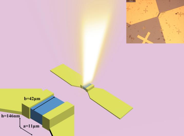
THz technology has attracted great attention in recent years,because of its wide application in many fields,such as medicine,biology,weather forecast,and environmental protection. Different detection mechanisms have been proposed[14-18]. Cai,X. demonstrated a graphene thermoelectric terahertz photodetector with sensitivity exceeding V/W and noise-equivalent power less than [19]. Recently,high sensitivity detection of terahertz waves was achieved with a graphene nanomesh as grating to improve the coupling efficiency of the incident terahertz waves and using a graphene nanostructure energy gap to enhance the excitation of plasmon. The sensitivity of the detector is 2.5 A/W[20]. A hot carrier-assisted photoconduction has been reported in homogeneous graphene,which shows sensitivity over and noise-equivalent power less than at room temperature[21].In this paper,a novel photoconductivity mechanism for THz detection is proven to be applicable for the design of a metal-GN-metal detector[22,23]:Consider a metal-GN-metal structure as shown in Figure 1. The spacing length and the width are and ,respectively. The thickness of the GN is. In the metal-GN-metal structure,there are two electric field configurations that are either symmetric or anti-symmetric with respect to the electrodes. Only anti-symmetric one has contribution to form potential wells and further trap carriers. The variation of the electron concentration can be further written according to the deduction by the electromagnetic induced well(EIW)theory[22]. When THz wave irradiates the GN mesa,electrons are driven from metals into the GN mesa. An EIW is generated by anti-symmetric electric field between the two metallic contacts and traps electrons from the metals in the well,then the conductivity of the GN mesa is changed and voltage signal is able to be detected. By taking advantage of the EIW photoconductivity effect,we achieve room-temperature sub-THz detection based on graphite nanosheets with sensitivity exceeding V/W( A/W)and noise-equivalent power of at room temperature.
Figure 1.The schematic diagram of the metal-GN-metal structure
The graphite nanosheets were peeled off from bulk graphite crystal by the way of micro-mechanical exfoliation using scotch type. After that,the nanosheets were transferred onto a high resistance Si substrate(>10000). The nanosheets could be identified by the optical microscope and the thickness of the flakes could be measured by atomic force microscope(AFM)as shown in Figure 2.
Figure 2.AFM images of two opposite interfaces between graphite nanosheet and Si substrate,the two-step heights between graphene nanosheets and high resistance Si are calculated by the difference of the maximum peak height and minimum peak height,the two-step heights are 148 nm(left picture)and 144 nm(right picture)respectively
Ti(),and Au()electrodes were evaporated on the top of the GN. The evaporation mask was fabricated using standard UV lithography. Metal-GN-metal structure was used to form an electromagnetic induced well(EIW)in graphite nanosheets. Both the top and the two side walls of the GN were covered in order to prevent the leakage of electromagnetic waves from the two sides and achieve a large optical gain. The width of the metal antenna was 0.5 mm and the total length of the metal antenna was 4 mm. The active receiving area of the device was 1142 and the thickness was 146 on average. The gap length(11)was close to the distance designed.
The Terahertz test system is established for sub-THz detection,as shown in Figure 3. In order to measure the sensitivity of the detector precisely,we use the solid-state frequency multiplication source produced by VDI Corporation(USA)that can emit continuous terahertz waves to radiate terahertz waves of 165-173 GHz. We also use lock-in amplifier to record the photo-response of commercial detector. The distance between THz source and our detector,the horn diameter()and the detection wavelength()are set up to satisfy the condition:. And the effective receiving area of the detector is far less than the area of the diaphragm. An adjustable diaphragm is placed in front of the commercial to calibrate the uniformity of the spot. We adjust the size of the diaphragm to get different voltage responses. The test data shows that the voltage response of the commercial is approximately linear to the area of the diaphragm,so we consider the field contribution is uniform. The power density of microwave source(20-40 GHz)is estimated by the total output power and the microwave filed area in the place of the detector when we ignore the transmission efficiency and microwave field uniformity. The power density is 0.88 for 0.035 THz and 0.15 for 0.1673 THz,respectively. The polarization direction of the incident THz wave which is specified in the experimental set up is perpendicular to the metal surface in order to get the high responsivity.
Figure 3.The schematic diagram of Terahertz test system
Figure 4(a)shows the I-V curve of the detector. The linear fit of I-V curve indicates a good ohmic contact between graphene and metal electrodes. Therefore,the depolarization field and the resistance of the interfaces can be ignored. The derived resistance of the device is about 110 Ω.
Figure 4.(a)The I-V curve of the detector,(b-c)the responsivity of the detector at the source frequency of 0.02-0.04 THz and 0.165-0.173 THz with the bias voltage of 0.1V,respectively,(d)the noise spectrum at the frequency from 250 Hz to 100 kHz with the bias voltage from 0.1 V to 0.01 V
It is important to confirm the effective receiving area for estimating the performance of the detector. In all kinds of THz detector based on graphene,different methods of calculating the effective receiving area have been used. In plasma-wave-assisted mechanism in Field effect transistors(FETs),photoinduced voltage is derived from the amplitude of radiation induced modulation of the source to gate voltage,which is originating from the metal antenna,so the antenna effect must be considered[14,24,25](diffraction limited area is commonly used to get a lower responsivity[26,27]). However,for photo-thermoelectric effect(PTE),the thermoelectric voltage(Seebeck effect)is induced by the temperature gradient caused by nonuniform illumination. For PTE detectors,the effective receiving area is considered to be the real material area,and diffraction limited area is also used as an estimation[19,28].
Here we measure the resistance change of the GN,which depends on the change in carrier mobility or carrier concentration. In the latter discussion,we exclude the bolometric effect of this detector,so the resistance change comes from variation of carrier concentration. It is caused by the electrons trapped in the GN by the EIW. Thus,we consider the effective receiving area should be the GN material area between the electrodes. In order to further prove this point,two points have been stated:(1)we have made the semiconductor devices with different sizes. It is found that the voltage response is proportional to the material area and is independent on the antenna area(not shown here).(2)we have considered the portion of metal on the mesa,because the electrons wrapped in the GN come from the metals. This small part of metal contributes to the increase in the conductance of the detector and is small enough to be ignored during calculating the effective receiving area. Of course,the metal antenna is supposed to be considered because of its contribution to the increasing of power density which is shown as gain factor(). Therefore,we calculate the responsivity according to formula(1) as follows:
.
In formula(1), originates from the Fourier transform of the square-wave modulated signal detected as rms value with a lock-in amplifier[21]. is the voltage response signal of the detector to sub-terahertz wave. is the power density of incident light and is the effective receiving area of the detector. is the gain factor of the structure. Here,we refer to the gain of 0.8 at 0.15 THz and 1.73 at 0.0375 THz in Ref.[22]using software simulations.
As shown in Figure 4(b)and Figure 4(c),the peak of responsivity appears at 0.035 THz and reaches around 20 kV/W in the 0.02-0.04 THz,while another peak value appears at 0.1673 THz and reaches around 11 kV/W in the 0.165-0.173 THz. As shown in Figure 4(b),the regular fluctuation between 0.034-0.036 THz is due to the interference caused by the thickness of Si substrate,which is about 0.4 mm. The oscillation with faster period in Figure 4(c)is resulted from the interference caused by the distance between the RF source and Si substrate,which is about 200 mm.
NEP is a key parameter to evaluate the performance of the detectors in consideration of noise characteristic,as the noise of the detector should be suppressed. The noise signal of our detector was recorded by a spectrum analyzer(MODEL SR 770). The modulation frequency was set to cover from 250 Hz to 100 kHz,and the bandwidth was 250 Hz. Firstly,we measured the short noise()when the circuit was shorted,and then connected the detector into the circuit for measuring the total noise(),finally we calculated the detector noise()by using a simple mean square root formula[29]:
.
NEP is calculated by formula(3) as follows:
.
In this formula,is the responsivity of the detector mentioned above. Different noise spectra of the detector were measured by varying the operating voltage(0.01 V,0.02 V,0.05 V,and 0.1 V). As shown in Figure 4(d),the total noise()was dominated by the detector in low f,since the -f curve varies with increasing bias voltage(). In contrast,the -f curves at different overlap with each other in the range of 20 kHz to 100 kHz,indicating the dominating factor of preamplifier noise. The -f character of the detector fits well with the 1/f law at low f,which is more than an order larger than the Johnson noise. The detector noise()is 92 at 1 kHz,and 25 at 10 kHz. During the calculation,the NEP of our detector is smaller than 4.6 for 0.035 THz and 9.2 for 0.1673 THz at 1 kHz. Under the same modulation frequency of 10 kHz,the NEP of the detector is about 1.25 for 0.035 THz and 2.27 for 0.1673 THz.
The time constant represents the speed of a detector responding to an incident electromagnetic wave. The value of time constant is defined as the time from the moment the incident light irradiated onto the surface of the detector to the moment that the signal reaches 63 percent of the maximum rise(fall).
.
When ,. is the time constant. Here,we record the waveform at a modulation frequency of 1 kHz by an oscilloscope and the waveform is shown in Figure 5(a). By using the impulse response method,we calculate the response time constant of the detector,which is approximately 700 ns for the rise edge and 1.5 μs for the drop edge.
Figure 5.(a)The waveform of the detector and time constant derivation from the waveform at 0.035 THz with the modulation frequency of 1 kHz,(b)the frequency dependent responses of the detector with different bias voltage(0.01 V,0.02 V,0.05 V and 0.1 V)at the source frequency of 0.035 THz,(c-d)the responsivity of the detector under different bias voltages at the source frequency of 0.035 THz and 0.1673 THz with the modulation frequency of 1 kHz,respectively
Figure 5(b)shows the response change trend of the device with modulation frequency at different bias voltages from 0.01 V to 0.1 V at 0.035 THz source radiation. As shown in Figure 5(c-d),the responsivity changes with the bias voltage at a modulation frequency of 1 kHz. Such linear dependency of the voltage response on the bias voltage can be observed in Figure 5(b-d). A significant voltage response was experimentally observed,while it could not be explained by the plasma-wave-assisted mechanism in FETs(Field Effect Transistors)nor photo-thermoelectric effect(PTE). To clarify the mechanism of the detector,we further discussed the change in resistance caused by bolometric effect.
2.2 Discussion on detection mechanism
Bolometric effect is an important effect in graphite and graphene,so it is necessary to confirm if the voltage response is dominated by the bolometric effect. First,hot electron effect plays an important role in graphene and graphite. The strong e–e interactions will lead to ultrafast heating of the electron. Thus,an effective temperature of electron remains higher than that of the lattice for femtosecond timescale. The electron-phonon scattering occurs for a slower time of several picoseconds. The hot electron concept described in the above is justified if the inequality relation below is satisfied with a conductor of size:[30]
,
here,is the diffusion length of electrons for electron-electron equilibration,where is the electron-electron scattering time and is the diffusion constant with the average speed of electrons and the momentum relaxation time. is the diffusion length of electrons for electron-phonon equilibration,where is the electron-phonon energy relaxation time. The half of the inequality relation,,requires that a low rate of electron-phonon scattering,which leads to a nonequilibrium state between electrons and the lattice,yielding the effective electron temperature higher than that of the lattice. A life-time estimate of electron-phonon scattering in graphite is 7 ps for THz pulses[31]. Electron effective velocity in graphite is in first-principles calculations[32]. We estimate ,here is the mean free path of electrons, and [33]. Hence,we get a calculation of the diffusion length of electron and . In our device,the channel length()is much larger than the diffusion length. The rate of electron-phonon scattering is so frequent that electrons are equilibrated with the lattice,yielding the effective electron temperature equivalent to the lattice temperature. Therefore,the hot electron effect can be ruled out in this device.
Next,we made an estimation for the temperature rise in order to eliminate the bolometric effect in our detector. We neglected the thermal conductivity of the graphene material,and assumed that the photon energy was completely converted into thermal energy and the detector was in a thermally insulated state for estimating the temperature rise of the material. Thus,formula(6) can be written as follows:
,
where is the mass of the material, is the specific heat capacity of graphite(710 ),is the response time of the detector,and is the power from the sub-THz source. Considering that the energy of the THz source can be coupled to the active element by the metal electrodes,the effective power can be enlarged because of field enhancement. The field enhancement is simulated to be close to 1 because the permittivity values of graphite and metal are close to each other. If the device is dominated by the bolometric effect,the voltage signal is estimated to be V,which is two orders smaller than the measured value in magnitude. The large difference indicates that bolometric effect does not play an important role in this detection.
The responsivity of the device is linear with the bias voltage,which is consistent with the expected results of the EIW theory. The increasing of the bias voltage means a larger internal bias field,thus the EIW generated in the GN will wrap more electron from metal electrode,which explains the linear behavior of responsivity with bias voltage. According to the formula of EIW,the responsivity of this device is supposed to be 60.5 kV/W,which is the same order with the responsivity according to experimental data,so we consider that EIW theory is a reasonable explanation for the voltage response of the detector. Table 1 compares the performance of different graphene-based detectors[19-21,27,28,34-37] and our detector has higher responsivity and lower NEP than the detectors reported.
Detection Mechanism
Responsivity
()
NEP
Frequency
(THz)
Effective area
Reference
EIW
11000
2.27
0.17
Real area
This work
Photoconduction assisted by hot-carriers
400
500
0.15
Real area
[21]
PTE
10
1100
2.5
Real area
[19]
PTE
105
80
1.8-4.25
Diffraction limited area
[28]
PTE
-
1000
2.8
Diffraction limited area
[34]
GFET
1.2
2000
0.29-0.38
Diffraction limited area
[27]
GFET
2.5A/W
-
3
Real area
[20]
GFET
14
515
0.6
-
[35]
GFET
30
120
3.4
Diffraction limited area
[36]
Nanoporous Graphene
-
424
1.4
-
[37]
Table 1. Comparison of responsivity and NEP of room temperature graphene or graphite nanosheet detectors designed with different mechanisms
In summary,a room-temperature sub-THz detector with high responsivity has been fabricated based on a simple metal-GN-metal structure. We have used graphite nanosheets to increase the optical absorption of the material. The EIW mechanism has been used to explain the THz detection based on the metal-GN-metal detector,while the contribution of bolometric effect has been excluded. Since the NEP performance declines slightly from 0.035 THz to 0.17 THz,it is expected that its detection performance for higher THz frequencies can be further improved by using ultrashort channel length of GN mesa,or by increasing the coupling effect between the electrodes and the GN material.
Jiang-Wei YAN, Xiao-Dong ZHANG, Wei ZHOU, Wan-Li MA, Tao HU, Niang-Juan YAO, Lin JIANG, Zhi-Ming HUANG. Room-temperature THz detection via EIW effect based on graphite nanosheet[J]. Journal of Infrared and Millimeter Waves, 2022, 41(3): 551