
Ahmed E. Hassanien, Steffen Link, Yansong Yang, Edmond Chow, Lynford L. Goddard, Songbin Gong. Efficient and wideband acousto-optic modulation on thin-film lithium niobate for microwave-to-photonic conversion[J]. Photonics Research, 2021, 9(7): 1182
- Photonics Research
- Vol. 9, Issue 7, 1182 (2021)
Abstract
1. INTRODUCTION
The development of photonic integrated circuit (PIC) applications prompted by optical transceivers for data centers, microwave photonic-based signal processing, quantum computing, spectroscopy, and holography, demands more efficient means to control lightwave propagation. One efficient method to achieve this objective is to utilize light–matter interactions through acousto-optic (AO) devices. Fundamentally, AO devices enable the interaction by perturbing the refractive index in an optical medium by acoustic waves [1]. The perturbation is made possible by the photoelastic effect in the medium, where acoustic and optical waves can be launched and guided independently. Several practical bulk-wave AO devices have been realized, including optical modulators, frequency shifters, switches, tunable filters, isolators, spectrum analyzers, scanners, and correlators [2].
Compared to electro-optic (EO) modulators that can operate efficiently with a low-pass characteristic and bandwidth (BW) up to tens of gigahertz [3,4], AO modulators can be ultra efficient and be boosted by the mechanical quality factor with bandpass frequency selectivity. Moreover, EO modulators typically have close electrode placement to the optical waveguides (WGs) to achieve high modulation efficiency and consequently do so at the expense of increased optical loss. On the other hand, AO modulators can have their interdigitated transducers (IDTs) placed far from the optical WGs without compromising efficiency and harness the low propagation loss of acoustic waves for strong AO interaction [5]. Whereas EO modulators are usually used for data transmission because of their wide BW, AO devices on different substrates might thrive complementarily for other applications, including modulators [6–9], frequency shifters [10,11], and tunable filters [12] and applications spanning phase-sensitive imaging [13], 3D holography [14], beamforming and steering [15], cavity optomechanics [16–18], and inertial sensing [19].
The vast outgrowth of research on guided wave optics and acoustics granted the ability to confine both the light and acoustic waves to the surface of a suitable substrate, resulting in PIC miniaturization and efficient light control. Surface wave AO devices possess significant advantages over discrete bulk AO devices. For example, surface wave devices feature smaller size and lighter weight with a high degree of integration, enabling batch processing and lower cost. They also have wider BW, lower power consumption, and larger overlap between acoustic and optical modes. Piezoelectric thin films such as gallium arsenide (GaAs) and lithium niobate (, or LN) are promising candidates for AO devices. These films have a high refractive index contrast to their surroundings for lightwave confinement and are compatible with generating acoustic waves using simple IDTs [20].
Sign up for Photonics Research TOC. Get the latest issue of Photonics Research delivered right to you!Sign up now
The advances of microwave photonics have recently been accelerated by unprecedented microwave-to-photonic conversion demonstrated in thin-film LN on insulator. LN is a synthetic crystal known for its various properties, such as the strong EO, photoelastic, and piezoelectric effects [21,22]. These properties are useful for linear and nonlinear optical applications and the generation and detection of acoustic waves. Moreover, LN has a negative uniaxial birefringence with a high refractive index ( at 1550 nm) and a high index contrast to many dielectrics, permitting strong confinement of optical modes and PIC miniaturization. LN thin-film on insulator (LNOI), a revolutionary technology, became recently available through smart-cut technology [23], giving rise to a myriad of new devices and applications with a high level of integration and performance.
In previous research efforts [18,20,24,25], optical WGs are inserted into resonant acoustic cavities, producing efficient AO modulators but sacrificing BW () and limiting their applicability for most real-world microwave signal-processing applications. In this work, we employ traveling acoustic waves to pass through the optical WG, eliminating the resonant nature in prior approaches, and resulting in highly desirable wideband modulators [26]. This approach provides filtration to the input microwave signal without any additional circuitry due to the bandpass spectral response of the microwave transducers, which makes it a perfect candidate for 5G and internet of things (IoT) applications where an optical signal is used for direct communication between 5G base stations and data centers [27]. Other applications, such as frequency comb generation, can also benefit from wideband and efficient AO modulators [28,29].
In this work, we present the design, implementation, and measurements of an efficient AO modulator using an unbalanced Mach–Zehnder interferometer (MZI) on thin-film LN (TFLN). The thin film is fully suspended, enabling the generation of Lamb acoustic waves (plate waves) that possess higher electromechanical coupling than surface acoustic waves (SAWs), resulting in significantly more efficient microwave to acoustic conversion. Acoustic modes are confined within the suspended film by the velocity mismatch boundary condition at the LN/air interface. On the other hand, optical modes are confined to the plane by the index contrast at the LN/air interface and guided laterally by a photonic crystal (PhC) WG made of a square lattice of air holes inside the LN suspended film [30]. The confinement of waves within the thin film features a unity overlap between the acoustic and optical modes, resulting in the efficient microwave-to-photonic conversion [18]. AO modulators with a phase shift up to , a center frequency of 1.9 GHz, and a BW up to 140 MHz were demonstrated. Moreover, a narrowband AO modulator with an optical WG inserted inside an acoustic cavity is reported in this paper to be compared with the state-of-the-art (SoA) AO modulators.
2. DESIGN METHODOLOGY
Figure 1(a) shows a mock-up of the proposed concept of this paper. A PhC WG is made of a square lattice of air holes with a periodicity of inside the TFLN. It is used to confine the light waves while allowing the acoustic waves to pass through. With a pitch of and split fingers, a split IDT is designed to generate mode Lamb waves at a center frequency of 1.9 GHz [31,32]. The frequency is selected to avoid working in the acoustic bandgap region of the PhC (centered around 4.2 GHz), allowing the acoustic waves to propagate through the optical WG with minimal reflection [33].
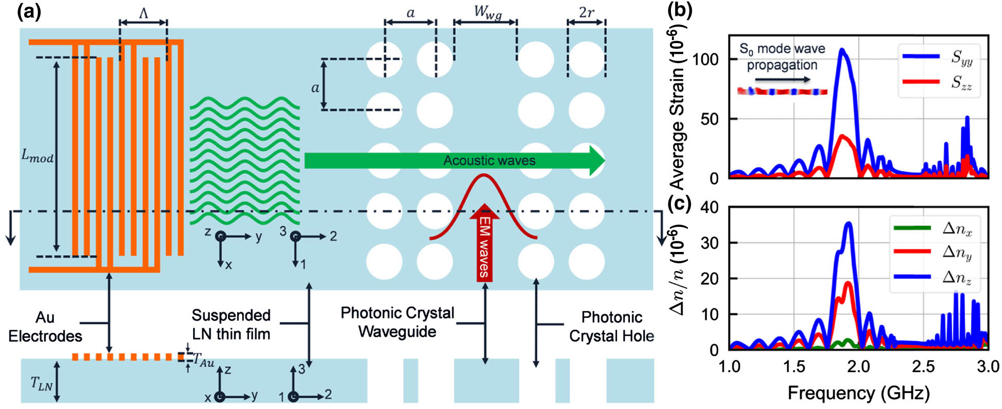
Figure 1.(a) Mock-up of the proposed AO modulator concept; (b) simulated average strain on 1 μm wide 560 nm thick optical WG; (c) total refractive index variation, in principal directions, due to simulated strain in (b).
The acoustic mode and LN cut were selected as and -cut for optimal optical waveguiding and aligning the highest strain component with the maximum photoelastic coefficient (). -cut LN is isotropic in-plane in both refractive index and photoelastic effect, allowing flexible layout of optical WGs. In comparison to other cuts of LN, it also has the highest and (0.138) for modulating the fundamental transverse magnetic (TM)-mode (z-polarized) by the acoustic mode (in-plane polarized). The average simulated strain on the optical WG is shown in Fig. 1(b) for a PhC WG with , hole periodicity , hole radius , and an applied radio frequency (RF) power of 1 mW (50-Ω source).
The change in refractive index , derived in Appendix C, can be calculated approximately using the following equation:
To demonstrate the proposed concept, an MZI on TFLN was designed and fabricated where only a single arm is acoustically modulated. The MZI is composed of focused grating couplers for input/output light coupling to fiber, multimode interferometers (MMIs) to split/combine light waves in the MZI arms, and WG crossings (WGCs) used as mechanical tethers for the suspended WG. A microscope image of the fabricated MZI is shown in Fig. 2(a). The optical response of the fabricated MZI was measured using the setup in Fig. 2(b). The response is shown in Fig. 2(c). A free spectral range (FSR) of 10.3 nm and an extinction ratio (ER) of 20 dB were observed. Figure 2(d) shows a cross-sectional scanning electron microscope (SEM) image of the fabricated WG along with the simulated values of the refractive and group indices of the TM mode (at 1550 nm). The simulation accounts for 65° sidewalls, resulting from the nature of the physical etching process.
![]()
Figure 2.(a) Microscope image of the fabricated MZI; (b) measurement setup for the optical response of the MZI device. EDFA, erbium-doped fiber amplifier; FPC, fiber polarization controller; DUT, device under test; DAQ, data acquisition card. (c) Measured optical response of the MZI; (d) cross-sectional SEM image of the optical WG (left) and simulated TM mode shape, including WG sidewalls (right).
The propagation loss of acoustic waves is relatively low. In our demonstration, the acoustic wave propagates only for a few tens of micrometers. It is estimated that the propagation loss of at 1.9 GHz is around 4 dB/mm [5]. The PhC WG is estimated to have loss for its 45 μm length (33 dB/mm) at 1550 nm based on finite-difference time-domain (FDTD) simulations. The loss can be improved by selecting an optimal periodicity (), which is beyond our in-house fabrication capabilities. On the other hand, rib WGs have based on FDTD simulations. The insertion loss due to mismatch between the rib and PhC WGs is by optimizing both the periodicity and WG width. The insertion loss can be further improved by WG tapering. All loss values are simulation-based and expected to be higher due to fabrication nonidealities such as sidewall angles and roughness resulting from the dry etching in the fabrication.
In this paper, we demonstrate two types of AO modulators. The first is a modulator without any acoustic cavity, resulting in wideband operation. The second is a modulator with one arm of the MZI inserted in a resonant acoustic cavity, resulting in a much more efficient modulation but narrowband operation. The main objective of the resonant device is to compare its performance to SoA AO modulators with similar configurations.
3. EXPERIMENTAL VALIDATION
A. Fabrication Process
The detailed fabrication process steps are shown in Fig. 3(a). The fabrication process starts with transfer-bonding Z-cut single-crystal TFLN (0.56 μm thick) to a silicon carrier (500 μm) with an intermediate layer of (4 μm) using the ion-slicing technique [34]. After that, using electron beam lithography, the IDTs are defined by lifting off 50 nm evaporated Au with 5 nm Cr adhesion layer. Next, a photoresist layer is spun and patterned using electron beam lithography as the soft mask for defining the release windows, PhC WG, gratings, and other optical components. An inductively coupled plasma with Ar-based reactive ion etching is then used to etch through the TFLN. Finally, the resonator is released using buffered oxide isotropic etching (BOE) to remove the sacrificial layer underneath the TFLN. Figure 3 shows SEM images of the various optical components and IDTs.
![]()
Figure 3.(a) Fabrication process. BOX, buried oxide; PR, photoresist. SEM images of (b) IDTs and modulated MZI arm; (c) PhC WG; (d) etched region used to protect the unmodulated MZI arm from the acoustic waves; (e) zoomed-in IDTs; (f) zoomed-in IDTs and PhC WG; and (g) WGC used for mechanical tethering.
Acoustic protection is added near the unmodulated MZI arm to protect it from the incident acoustic waves that have already passed through the modulated arm. As shown in Fig. 3(d), the acoustic protection is achieved by etching LN with a geometrical shape, causing incoherent scattering of the acoustic wavefront and acoustic wave dissipation in the form of heat. This prevents reflected acoustic waves from interacting with the modulated arm again. Figure 3(g) shows the WGC used to add mechanical tethers to the WG. Each WGC is optimized to have less than 0.1 dB of optical insertion loss.
B. Measurement Approach
The AO modulator was measured using a two-port network analyzer, as shown in Fig. 4(a). Port 1 is used as a power source to excite the acoustic waves connected to the RF pads shown in Fig. 2(a), while Port 2 measures optical . Port 2 can be connected to a spectrum analyzer, in case of measuring power at DC. Grating couplers were designed to have coupling efficiency at 1550 nm, but their values are expected to deviate (estimated coupling efficiency from measurements ), resulting from our lithography fidelity and sidewall roughness from dry etching. An erbium-doped fiber amplifier (EDFA) is used to boost the input laser to 27 dBm to compensate for optical losses due to grating couplers and PhC WGs. A fiber polarization controller (FPC) is used to adjust the input light to the TM mode. A photoreceiver (PR) with an internal transimpedance amplifier (TIA) and a responsivity of 1625 V/W is used.
![]()
Figure 4.(a) Measurement setup; (b) measured optical powers versus wavelength for device A; (c) measured
One arm of the MZI is phase-modulated by the acoustic waves, while the other arm is not modulated, resulting in an amplitude-modulated light signal. The phase shifts due to refractive index perturbation caused by the acoustic wave and the initial phase mismatch between MZI arms representing any imbalances , derived in Appendix A, can be expressed as
By measuring , can be calculated as follows:
C. Results
Figure 4(b) shows the measured optical power at DC () and at the fundamental () of device A, whereas dimensions of different devices reported in this article are shown in Table 1. As the wavelength is swept in Fig. 4(b), the phase difference between the MZI arms () changes, resulting in power fluctuation dependent on the phase mismatch between the MZI arms. Figure 4(c) shows measured scattering parameters and of device A. The device has a center frequency of 1.9 GHz and wide BW of 140 MHz (fractional BW of 7.4%), both of which match their respective values estimated by simulations. can be extracted from Eq. (9), resulting in a highly efficient AO modulator with a figure of merit (FoM) of where . Noteworthily, is used only to compare AO modulators to EO modulators [3,35], but a more convenient FoM is representing the power needed by the transducer (IDTs) to achieve phase shift multiplied by the modulation length. Another suitable FoM is presenting the phase shift of the light wave per unit length per square root of the applied power, where presents the amount of phase shift acquired by the square root of the applied power, . Fabricated Devices’ DimensionsDevice A 25 2.9 45 0.7 1 0.35 0.56 50 B 49 2.9 45 0.7 1 0.35 0.56 50 C 7 2.8 45 0.7 1 0.35 0.56 50
![]()
Figure 5.(a) Measured
4. DISCUSSION
Table 2 compares fabricated devices in this paper to SoA AO modulators. Device C, which is mainly used for comparison to SoA, as it has an acoustic cavity, is a highly efficient narrowband AO modulator with of 0.15 mW · cm, which has more efficient modulation compared to the nearest AO modulator [18]. The modulation efficiency can be traded-off for BW, as seen in devices A and B having more than the BW reported in the literature. For the wideband devices A and B, the sinc-function-shaped spectrum shown in Figs. 4(c) and 5(a) is a characteristic of the IDTs. The spectrum can be tailored to reduce the strength of the sidelobes and to produce a steeper roll-off by apodizing the IDTs [36].
Enhancement to AO modulation efficiency is achieved, in this paper, by using Lamb waves, utilizing the highest photoelastic coefficients in LN, and optimizing the light–acoustic interaction by selecting the optimum orientation. Moreover, there is still room for significant improvements by performing simple modifications to the design. First, the IDTs used in this paper are split IDTs that are inherently bidirectional, which means they direct acoustic waves equally on both sides of the IDT, resulting in an inherent 3-dB loss. This can be avoided by using unidirectional IDTs [36,38] that direct the acoustic power in one direction towards the WG. Second, the MZI presented in this paper has only a single arm experiencing modulation, while a push–pull MZI configuration can boost modulation efficiency [20,24,25,37].
5. CONCLUSIONS
We demonstrated a wideband AO modulator on suspended TFLN. The modulator has a passband with a center frequency at 1.9 GHz, and a BW of 140 MHz. The device is highly efficient with and a modulation length of only 45 μm [i.e., ]. Unlike conventional AO modulators with a narrow BW, this device is both efficient and wideband; therefore, it is highly practical for many microwave photonic applications. Moreover, a resonant device with an acoustic cavity is compared to the SoA AO modulators, showing a more efficient modulation. The enhancement arises from exploiting Lamb waves, using the highest photoelastic coefficients, and arranging the light–acoustic interaction in the optimal orientation.
APPENDIX A: DERIVATION OF MZI OUTPUT SPECTRUM
The electric field output at each arm () of the MZI is
APPENDIX B: DERIVATION OF Vπ, Pπ, and ap
The voltage required for a 180° phase shift, , can be directly calculated from the measured scattering parameter . Starting from Eqs.?(
APPENDIX C: ESTIMATION OF REFRACTIVE INDEX PERTURBATION
The refractive index change can be estimated by assuming two perturbation effects, the photoelastic and the EO effects. The perturbed index ellipsoid can be expressed as
References
[1] B. E. A. Saleh, M. C. Teich. Fundamentals of Photonics(2019).
[2] C. S. Tsai. Guided-Wave Acousto-Optics: Interactions, Devices, and Applications(1990).
[3] M. Bahadori, Y. Yang, A. E. Hassanien, L. L. Goddard, S. Gong. Ultra-efficient and fully isotropic monolithic microring modulators in a thin-film lithium niobate photonics platform. Opt. Express, 28, 29644-29661(2020).
[4] C. Wang, M. Zhang, X. Chen, M. Bertrand, A. Shams-Ansari, S. Chandrasekhar, P. Winzer, M. Lončar. Integrated lithium niobate electro-optic modulators operating at CMOS-compatible voltages. Nature, 562, 101-104(2018).
[5] R. Lu, T. Manzaneque, Y. Yang, M. H. Li, S. Gong. Gigahertz low-loss and wideband S0 mode lithium niobate acoustic delay lines. IEEE Trans. Ultrason. Ferroelectr. Freq. Control, 66, 1373-1386(2019).
[6] S. A. Tadesse, M. Li. Sub-optical wavelength acoustic wave modulation of integrated photonic resonators at microwave frequencies. Nat. Commun., 5, 5402(2014).
[7] S. A. Tadesse, H. Li, Q. Liu, M. Li. Acousto-optic modulation of a photonic crystal nanocavity with Lamb waves in microwave K band. Appl. Phys. Lett., 107, 201113(2015).
[8] S. Ghosh, G. Piazza. Laterally vibrating resonator based elasto-optic modulation in aluminum nitride. APL Photon., 1, 036101(2016).
[9] M. Mahmoud, L. Cai, A. Mahmoud, T. Mukherjee, G. Piazza. Electro-optically controlled acousto-optic racetrack modulator etched in LNOI platform. IEEE International Conference on Micro Electro Mechanical Systems (MEMS), 743-746(2018).
[10] L. Fan, C. L. Zou, M. Poot, R. Cheng, X. Guo, X. Han, H. X. Tang. Integrated optomechanical single-photon frequency shifter. Nat. Photonics, 10, 766-770(2016).
[11] G. Fan, Y. Li, C. Hu, L. Lei, D. Zhao, H. Li, Z. Zhen. A novel concept of acousto-optic ring frequency shifters on silicon-on-insulator technology. Opt. Laser Technol., 63, 62-65(2014).
[12] W. Yang, Y. Liu, L. Xiao, Z. Yang. Wavelength-tunable erbium-doped fiber ring laser employing an acousto-optic filter. J. Lightwave Technol., 28, 118-122(2010).
[13] Z. Shen, X. Han, C. L. Zou, H. X. Tang. Phase sensitive imaging of 10 GHz vibrations in an AlN microdisk resonator. Rev. Sci. Instrum., 88, 123709(2017).
[14] G. Ryu, Y. Lee, K. Lee. Development of acoustic-optic (AO) SLM applicable to 3D holographic dispay. 19th International Conference on Solid-State Sensors, Actuators and Microsystems, 1979-1982(2017).
[15] M. N. Armenise, V. M. N. Passaro, G. Noviello. Lithium niobate guided-wave beam former for steering phased-array antennas. Appl. Opt., 33, 6194-6209(1994).
[16] W. Jiang, R. N. Patel, F. M. Mayor, T. P. McKenna, P. Arrangoiz-Arriola, C. J. Sarabalis, J. D. Witmer, R. V. A. N. Laer, A. H. Safavi-Naeini. Lithium niobate piezo-optomechanical crystals. Optica, 6, 845-853(2019).
[17] M. Aspelmeyer, T. J. Kippenberg, F. Marquardt. Cavity optomechanics. Rev. Mod. Phys., 86, 1391-1452(2014).
[18] L. Shao, M. Yu, S. Maity, N. Sinclair, L. Zheng, C. Chia, A. Shams-Ansari, C. Wang, M. Zhang, K. Lai, M. Lončar. Microwave-to-optical conversion using lithium niobate thin-film acoustic resonators. Optica, 6, 1498-1505(2019).
[19] M. Mahmoud, A. Mahmoud, L. Cai, M. Khan, T. Mukherjee, J. Bain, G. Piazza. Novel on chip rotation detection based on the acousto-optic effect in surface acoustic wave gyroscopes. Opt. Express, 26, 25060-25075(2018).
[20] L. Cai, A. Mahmoud, M. Khan, M. Mahmoud, T. Mukherjee, J. Bain, G. Piazza. Acousto-optical modulation of thin film lithium niobate waveguide devices. Photon. Res., 7, 1003-1013(2019).
[21] R. S. Weis, T. K. Gaylord. Lithium niobate: summary of physical properties and crystal structure. Appl. Phys. A, 37, 191-203(1985).
[22] K. K. Wang. Properties of Lithium Niobate(2002).
[23] S. Gong, H. Bhugra, G. Piazza. Lithium niobate for M/NEMS resonators. Piezoelectric MEMS Resonators, 99-129(2017).
[24] M. M. De Lima, M. Beck, R. Hey, P. V. Santos. Compact Mach-Zehnder acousto-optic modulator. Appl. Phys. Lett., 89, 121104(2006).
[25] A. Crespo-Poveda, R. Hey, K. Biermann, A. Tahraoui, P. V. Santos, B. Gargallo, P. Muñoz, A. Cantarero, M. M. de Lima. Synchronized photonic modulators driven by surface acoustic waves. Opt. Express, 21, 21669-21676(2013).
[26] A. E. Hassanien, E. Chow, S. Link, Y. Yang, L. L. Goddard, S. Gong. Wideband acousto-optical modulation on suspended thin-film lithium niobate. Conference on Lasers and Electro-Optics(2021).
[27] K. H. Shakthi Murugan, M. Sumathi. Design and analysis of 5G optical communication system for various filtering operations using wireless optical transmission. Results Phys., 12, 460-468(2019).
[28] M. Zhang, B. Buscaino, C. Wang, A. Shams-Ansari, C. Reimer, R. Zhu, J. M. Kahn, M. Lončar. Broadband electro-optic frequency comb generation in a lithium niobate microring resonator. Nature, 568, 373-377(2019).
[29] A. Rueda, F. Sedlmeir, M. Kumari, G. Leuchs, H. G. L. Schwefel. Resonant electro-optic frequency comb. Nature, 568, 378-381(2019).
[30] J. D. Joannopoulos, S. G. Johnson, J. N. Winn, R. D. Meade. Photonic Crystals: Molding the Flow of Light(2008).
[31] B. A. Auld. Acoustic Fields and Waves in Solids(1973).
[32] D. Royer, E. Dieulesaint. Elastic Waves in Solids: Free and Guided Propagation(1996).
[33] R. Lu, T. Manzaneque, Y. Yang, S. Gong. Lithium niobate phononic crystals for tailoring performance of RF laterally vibrating devices. IEEE Trans. Ultrason. Ferroelectr. Freq. Control, 65, 934-944(2018).
[34] M. Levy, R. M. Osgood, R. Liu, L. E. Cross, G. S. Cargill, A. Kumar, H. Bakhru. Fabrication of single-crystal lithium niobate films by crystal ion slicing. Appl. Phys. Lett., 73, 2293-2295(1998).
[35] Y. Yang, M. Bahadori, A. E. Hassanien, L. L. Goddard, S. Gong. An isotropic lithium niobate microring resonator with a 1.38-nm wide continuous tuning range using 80 V. Conference on Lasers and Electro-Optics, JTh2F.27(2020).
[36] C. Campbell, J. C. Burgess. Surface acoustic wave devices and their signal processing applications. J. Acoust. Soc. Am., 89, 1479-1480(1991).
[37] M. S. I. Khan, A. Mahmoud, L. Cai, M. Mahmoud, T. Mukherjee, J. A. Bain, G. Piazza. Extraction of elastooptic coefficient of thin-film arsenic trisulfide using a Mach-Zehnder acoustooptic modulator on lithium niobate. J. Lightwave Technol., 38, 2053-2059(2020).
[38] R. Lu, Y. Yang, S. Gong. Low-loss unidirectional acoustic focusing transducer in thin-film lithium niobate. IEEE Trans. Ultrason. Ferroelectr. Freq. Control, 67, 2731-2737(2020).

Set citation alerts for the article
Please enter your email address
© Copyright 2018-2021 | Chinese Laser Press. All Rights Reserved 沪ICP备15018463号-20