• Photonics Research
  • Vol. 10, Issue 10, A135 (2022)
Lantian Feng1、2、3, Ming Zhang4, Jianwei Wang5、6, Xiaoqi Zhou7, Xiaogang Qiang8, Guangcan Guo1、2、3, and Xifeng Ren1、2、3、*
Author Affiliations
  • 1CAS Key Laboratory of Quantum Information, University of Science and Technology of China, Hefei 230026, China
  • 2CAS Center for Excellence in Quantum Information and Quantum Physics, University of Science and Technology of China, Hefei 230026, China
  • 3Hefei National Laboratory, University of Science and Technology of China, Hefei 230088, China
  • 4State Key Laboratory for Modern Optical Instrumentation, Centre for Optical and Electromagnetic Research, Zhejiang Provincial Key Laboratory for Sensing Technologies, Zhejiang University, Zijingang Campus, Hangzhou 310058, China
  • 5State Key Laboratory for Mesoscopic Physics, School of Physics, Peking University, Beijing 100871, China
  • 6Frontiers Science Center for Nano-optoelectronics, Collaborative Innovation Center of Quantum Matter, Peking University, Bejing 100871, China
  • 7School of Physics and State Key Laboratory of Optoelectronic Materials and Technologies, Sun Yat-sen University, Guangzhou 510000, China
  • 8National Innovation Institute of Defense Technology, AMS, Beijing 100071, China
  • show less
    DOI: 10.1364/PRJ.464808 Cite this Article Set citation alerts
    Lantian Feng, Ming Zhang, Jianwei Wang, Xiaoqi Zhou, Xiaogang Qiang, Guangcan Guo, Xifeng Ren. Silicon photonic devices for scalable quantum information applications[J]. Photonics Research, 2022, 10(10): A135 Copy Citation Text show less
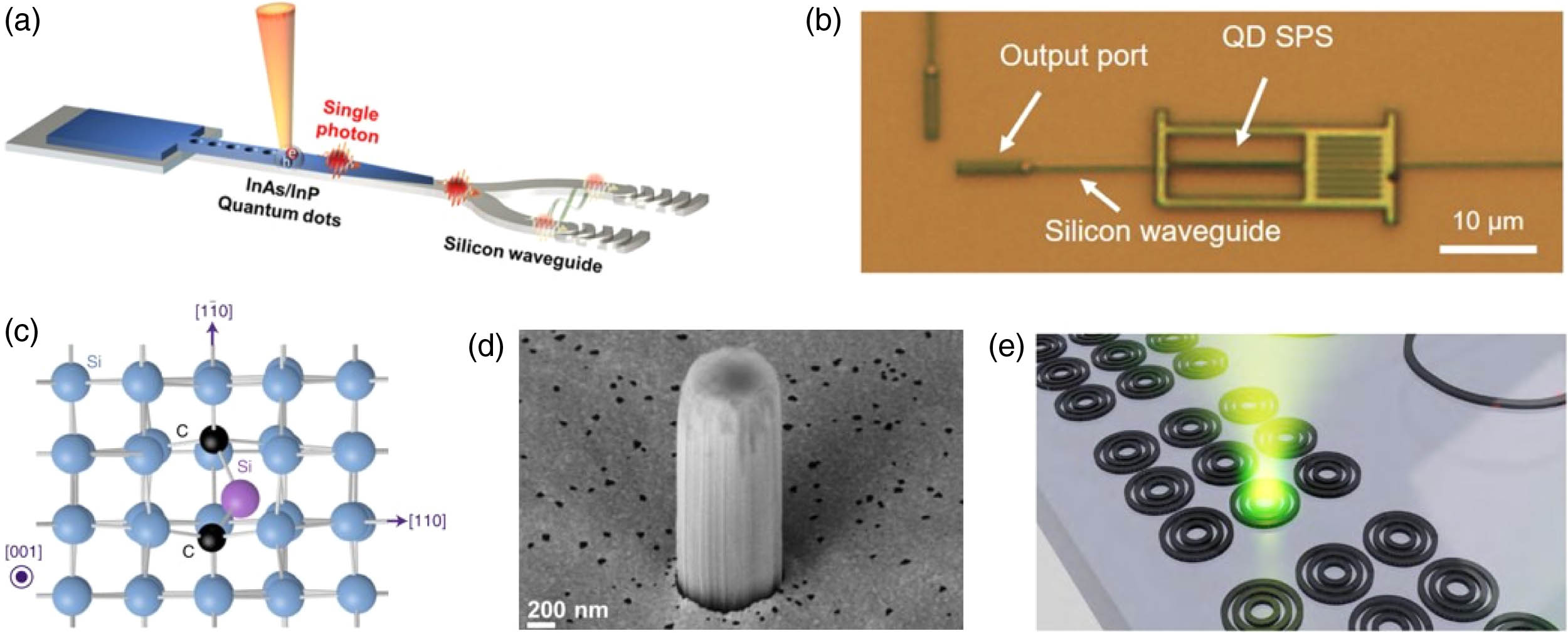
    Solid-state quantum emitters in silicon photonics. (a) Position grown InAs/InP quantum dots on a silicon photonic chip by the pick-and-place technique. Adapted from [59]. (b) Integrate heterogeneous optical components with a transfer-printing-based approach. Adapted from [62]. (c) Atomic structure of the G-center. Adapted from [63]. (d) Si nanopillar including the G-center. Adapted from [64]. (e) Bullseye structures used to enhance vertical coupling of G-centers. Adapted from [65].
    Fig. 1. Solid-state quantum emitters in silicon photonics. (a) Position grown InAs/InP quantum dots on a silicon photonic chip by the pick-and-place technique. Adapted from [59]. (b) Integrate heterogeneous optical components with a transfer-printing-based approach. Adapted from [62]. (c) Atomic structure of the G-center. Adapted from [63]. (d) Si nanopillar including the G-center. Adapted from [64]. (e) Bullseye structures used to enhance vertical coupling of G-centers. Adapted from [65].
    Integrated SNSPDs for single-photon detection. (a) Principle of traveling wave coupling. Adapted from [37]. (b) SNSPD within a high-quality factor microcavity. Adapted from [84]. (c) Cavity-integrated SNSPD. Adapted from [87]. (d) SNSPD implemented in a two-dimensional photonic crystal cavity. Adapted from [88]. (e) A typical chain of single-photon detector segments for signal multiplexing and number resolution. Adapted from [89].
    Fig. 2. Integrated SNSPDs for single-photon detection. (a) Principle of traveling wave coupling. Adapted from [37]. (b) SNSPD within a high-quality factor microcavity. Adapted from [84]. (c) Cavity-integrated SNSPD. Adapted from [87]. (d) SNSPD implemented in a two-dimensional photonic crystal cavity. Adapted from [88]. (e) A typical chain of single-photon detector segments for signal multiplexing and number resolution. Adapted from [89].
    Wavelength division multiplexing techniques in silicon photonics. (a) Cascaded Mach–Zehnder demultiplexer. Adapted from [105]. (b) The wavelength division multiplexing receiver chip with an integrated arrayed waveguide grating. Adapted from [110]. (c) Coupled five-ring silicon filter. Adapted from [111]. (d) Waveguide Bragg grating add-drop filter. Adapted from [112].
    Fig. 3. Wavelength division multiplexing techniques in silicon photonics. (a) Cascaded Mach–Zehnder demultiplexer. Adapted from [105]. (b) The wavelength division multiplexing receiver chip with an integrated arrayed waveguide grating. Adapted from [110]. (c) Coupled five-ring silicon filter. Adapted from [111]. (d) Waveguide Bragg grating add-drop filter. Adapted from [112].
    Mode division multiplexing techniques in silicon photonics. (a) Mode (de)multiplexer with adiabatic taper. Adapted from [125]. (b) Mode (de)multiplexer. Adapted from [126]. (c) Multiport multimode waveguide crossing using a metamaterial-based Maxwell’s fisheye lens. Adapted from [127]. (d) Digital metastructure-based multimode bending. Adapted from [128]. (e) High-speed optical two-mode switch. Adapted from [129]. (f) Reconfigurable optical add-drop multiplexer for hybrid wavelength/mode-division-multiplexing systems. Adapted from [124].
    Fig. 4. Mode division multiplexing techniques in silicon photonics. (a) Mode (de)multiplexer with adiabatic taper. Adapted from [125]. (b) Mode (de)multiplexer. Adapted from [126]. (c) Multiport multimode waveguide crossing using a metamaterial-based Maxwell’s fisheye lens. Adapted from [127]. (d) Digital metastructure-based multimode bending. Adapted from [128]. (e) High-speed optical two-mode switch. Adapted from [129]. (f) Reconfigurable optical add-drop multiplexer for hybrid wavelength/mode-division-multiplexing systems. Adapted from [124].
    Silicon photonic modulators at cryogenic temperatures. (a) The plasma dispersion microdisk modulator. Adapted from [138]. (b) The BaTiO3-Si racetrack resonator. Adapted from [139]. (c) The integrated PIN junction modulator and unbalanced Mach–Zehnder interferometer composed of the modulator. Adapted from [140].
    Fig. 5. Silicon photonic modulators at cryogenic temperatures. (a) The plasma dispersion microdisk modulator. Adapted from [138]. (b) The BaTiO3-Si racetrack resonator. Adapted from [139]. (c) The integrated PIN junction modulator and unbalanced Mach–Zehnder interferometer composed of the modulator. Adapted from [140].
    Chip interconnection techniques in silicon photonics. (a) Diffraction grating-based coupling structure. Adapted from [35]. (b) The focusing grating. Adapted from [146]. (c) The double-etched apodized waveguide grating coupler. Adapted from [147]. (d) The grating coupler with a single aluminum backside mirror. Adapted from [148]. (e) The mode-size converter as end coupler. Adapted from [149]. (f) Coupler structure. Adapted from [150]. (g) The 3D-printed optical probes on the fiber end faces. Adapted from [151]. (h) Fiber cores and different silicon waveguides connected by photonic wire bonds. Adapted from [152]. (i) In situ 3D nanoprinted free-form lenses and expanders. Adapted from [153].
    Fig. 6. Chip interconnection techniques in silicon photonics. (a) Diffraction grating-based coupling structure. Adapted from [35]. (b) The focusing grating. Adapted from [146]. (c) The double-etched apodized waveguide grating coupler. Adapted from [147]. (d) The grating coupler with a single aluminum backside mirror. Adapted from [148]. (e) The mode-size converter as end coupler. Adapted from [149]. (f) Coupler structure. Adapted from [150]. (g) The 3D-printed optical probes on the fiber end faces. Adapted from [151]. (h) Fiber cores and different silicon waveguides connected by photonic wire bonds. Adapted from [152]. (i) In situ 3D nanoprinted free-form lenses and expanders. Adapted from [153].
    Multiphoton and high-dimensional applications with silicon photonic devices. (a) Silicon photonic chip for the generation and sampling of quantum states. Adapted from [161]. (b) Coherent pumping of two sources and processing of the emitted photons. Adapted from [47]. (c) Chip-to-chip high-dimensional quantum key distribution based on multicore fiber. Adapted from [187]. (d) Silicon device for multidimensional quantum entanglement. Adapted from [188]. (e) Programmable qudit-based quantum processor. Adapted from [189].
    Fig. 7. Multiphoton and high-dimensional applications with silicon photonic devices. (a) Silicon photonic chip for the generation and sampling of quantum states. Adapted from [161]. (b) Coherent pumping of two sources and processing of the emitted photons. Adapted from [47]. (c) Chip-to-chip high-dimensional quantum key distribution based on multicore fiber. Adapted from [187]. (d) Silicon device for multidimensional quantum entanglement. Adapted from [188]. (e) Programmable qudit-based quantum processor. Adapted from [189].
    Quantum error correction with silicon photonic devices. Error-protected qubits for quantum computation. Adapted from [163].
    Fig. 8. Quantum error correction with silicon photonic devices. Error-protected qubits for quantum computation. Adapted from [163].
    Quantum key distribution (QKD) with silicon photonic devices. (a) Integrated devices for time-bin encoded BB84. Adapted from [209]. (b) Integrated devices for high-speed measurement-device-independent QKD. Adapted from [216]. (c) Silicon photonics encoder with high-speed electro-optic phase modulators. Adapted from [211]. (d) Detector-integrated on-chip QKD receiver. Adapted from [95].
    Fig. 9. Quantum key distribution (QKD) with silicon photonic devices. (a) Integrated devices for time-bin encoded BB84. Adapted from [209]. (b) Integrated devices for high-speed measurement-device-independent QKD. Adapted from [216]. (c) Silicon photonics encoder with high-speed electro-optic phase modulators. Adapted from [211]. (d) Detector-integrated on-chip QKD receiver. Adapted from [95].
    Quantum state teleportation with silicon photonic devices. Chip-to-chip quantum teleportation. Adapted from [162].
    Fig. 10. Quantum state teleportation with silicon photonic devices. Chip-to-chip quantum teleportation. Adapted from [162].
    ReferenceStructureBandwidthPGR/SERCARg2(0)Wavelength
    [43]Single-mode waveguide100 GHz0.7  MHz·mW2801538.2 and 1562.2 nm
    [44]Microring resonator2.1 GHz149  MHz·mW212,1050.005331535.5 and 1574.7 nm
    [47]bMultimode waveguide4 nm18.6  MHz·mW20.0531516 and 1588 nm
    [48]GaN defect3–50 nm1.5 MHz0.051085–1340 nm
    [49]b2D MoTe28.5–37 nm0.0581080–1550 nm
    [50]G center0.5 nm99 kHz0.071278 nm
    [51]T center255 MHz0.21326 nm
    Table 1. State-of-the-Art Photonic Sources at Telecommunications Wavelengthsa
    ReferenceDetection EfficiencyJitterDark Count RateReset TimeTemperatureNumber Resolving
    [37]91%18 ps50 Hz505 ps1.7 K
    [84]100%55 ps0.1 Hz7 ns2.05 K
    [87]30%32 ps1 Hz510 ps1.7 K
    [88]70%480 ps0.1 MHz480 ps1.6 K
    [91]5.6%b16.1 ps2 Hz85.8 ns1.0 K4
    [98]29.4%134 ps100 kHz125 K
    [100]60.1%340 kHz88 ns300 K
    Table 2. State-of-the-Art Techniques for Integrated Single-Photon Detectiona
    ReferenceStructureSizeContrastILFSRBandwidth
    [116]High-order microring700  μm240 dB1.8 dB18 nm310 GHz (1 dB)
    [111]High-order microring3000  μm250 dB3 dB7.3 nm11.6–125 GHz (3 dB)
    [115]Unbalanced MZIs2  mm215 dB9 dB0.8 nm0.61, 0.34, and 0.21 nm (3 dB)
    [112]WBG600  μm235 dB0.6 dB3 nm (3 dB)
    [119]Cascaded WBG1280  μm265 dB3 dB1–2 nm (3 dB)
    [120]Cascaded WBG3105  μm260 dB2 dB5.5 nm (3 dB)
    Table 3. State-of-the-Art Techniques for Filtering in Silicon Photonicsa
    Ref.TechniqueLossBandwidth
    [160]Grating coupling0.58 dB (TE)71 nm (3 dB)
    [165]End coupling (tapered fiber)0.36 dB (TM); 0.66 dB (TE)>80  nm (1 dB)
    [149]End coupling (SMF)2.0 dB (TM); 1.2 dB (TE)>120  nm (1 dB)
    [166]End coupling (SMF)1.3 dB (TM); 0.95 dB (TE)>100  nm (1 dB)
    [150]3D vertical coupling1 dB (TE and TM)170 nm (TE); 104 nm (TM) (1 dB)
    [151]3D printing1.9 dB
    [152,167,168]Wire bonding0.4 dB
    [153]In situ 3D nanoprinting0.6 dB
    Table 4. State-of-the-Art Techniques for Chip Interconnection in Silicon Photonicsa
    Lantian Feng, Ming Zhang, Jianwei Wang, Xiaoqi Zhou, Xiaogang Qiang, Guangcan Guo, Xifeng Ren. Silicon photonic devices for scalable quantum information applications[J]. Photonics Research, 2022, 10(10): A135
    Download Citation