Schematic view of topology-empowered membrane devices for terahertz photonics. Credit: Q. Yang et al., doi 10.1117/1.AP.4.4.046002
Terahertz photonics is an emerging field with great potential for biosensing, nondestructive imaging or detection, and next-generation communication technologies (beyond 6G). However, existing terahertz components and systems are bulky and sensitive to imperfections and transmission losses. Miniaturization and integration of photonic devices and systems may be achieved via meta-optics. Metadevices based on the free-standing dielectric membrane at the subwavelength scale are of practical importance as they remove many limitations experienced by devices on substrates.
Recent discoveries of photonic topological insulators reveal that such materials may support robust edge states immune to disorder and sharp corners. Early approaches to the topological phases relied on an external magnetic field or careful design, which has hindered widespread implementation. Meanwhile, researchers have invested efforts in valley-Hall photonics crystals (VHPCs), which support robust edge modes inside a photonic bandgap but do not require time-reversal symmetry breaking. The combination of meta-optics and topological photonics promises future terahertz topological on-chip photonic networks for next-generation wireless communications and quantum computing. Topological metadevices will enable development of a robust and efficient platform for terahertz on-chip communication, sensing, and multiplexing systems.
To this end, an international team of researchers from Australian National University, Central South University, and Oak Ridge National Laboratory recently developed a range of topological membrane metadevices for on-chip terahertz wave manipulations and demonstrated them experimentally. As reported in Advanced Photonics, they employed a unique terahertz double probe near-field setup to characterize the performance of topological devices—the first-ever such experiment for topological devices.

Image of terahertz topological metadevices and near-field setup. (A) Fabricated terahertz topological devices on a 4-inch SOI wafer. (B) Optical image of terahertz double-probe near-field scanning system and topological on-chip splitter. Credit: Q. Yang et al., doi 10.1117/1.AP.4.4.046002.
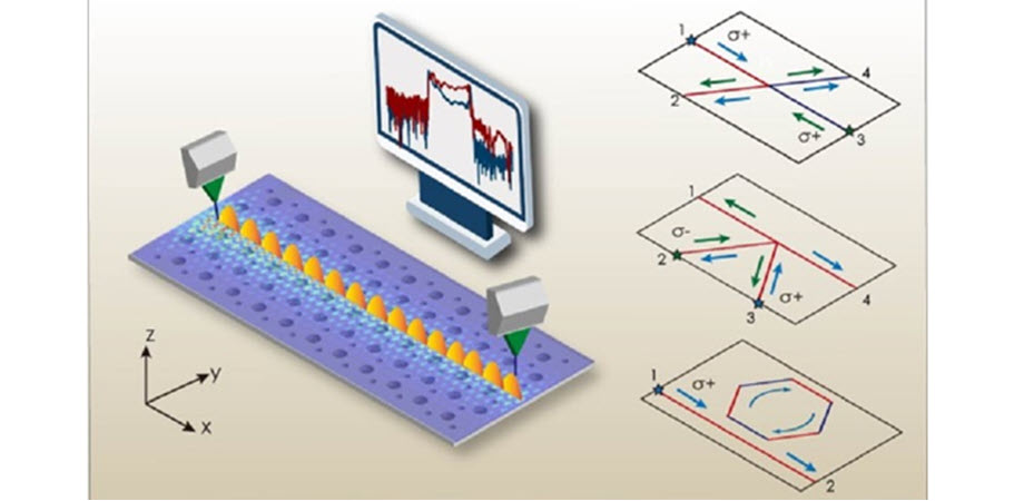
Topology-empowered metadevices bear some resemblance to their regular waveguide-based counterparts, yet exhibit some unique features due to the unidirectional propagation of given modes. The researchers showcase a series of topological waveguides, various couplers, splitters, and ring resonators at terahertz frequency, which allow robust single-mode on-chip terahertz wave manipulation.
Reportedly, the edge states at two types of domain walls are valley-locked, which prohibits intervalley scattering and supports the possibility to build various terahertz on-chip devices. According to senior author Ilya Shadrivov, professor at Australian National University, “These topological membrane metadevices open up novel capabilities for controlling terahertz waves on the chip. This will may bring terahertz on-chip devices to the next level and help to revolutionize future communication technologies.”
Read the Gold Open Access article by Q. Yang et al., “Topology-empowered membrane devices for terahertz photonics,” Adv. Photon. 4(4) 046002 (2022), doi 10.1117/1.AP.4.4.046002.