Original article: Stefania Castelletto and Alberto Boretti " Color centers in wide-bandgap semiconductors for sub-diffraction imaging"
Super-resolution fluorescence microscopy (SRM) has revolutionized the optical microscopy world, achieving nanometric resolution in optical imaging of biological structures with details approaching molecular structure sizes. Its combination with nanoscale magnetic resonance imaging (nano MRI) is a very sought-after goal in this area of research, motivated by the need to establish correlative imaging with high-resolution modality, combined with fast temporal dynamics sensing for early diagnostics and therapeutics.
In principle, this technique could enable detailed, real-time observation of internal and surface cellular processes, such as cell death, evolution and division, and how cells are affected by a disease or drug delivery. These methods can provide early detection of disease or aid in therapeutics study at the single-cell and subcellular level in combination with nanomedicine and drug delivery; they can be applied to study the interaction for example of viruses infecting living cells, advance the development of anti-viral therapeutics if some of the current limitations could be overcome.
Among these limitations, the nature of the fluorescent tags is of paramount importance to achieve the desired resolution in the cells' environment and to follow internal biological mechanisms in cells in specific locations. Ideal fluorescent tags must be photostable, interfere as little as possible with the biological systems, emit in a spectral region where cells autofluorescence is low, and be activated by low energy laser to reduce photodamage. Many methods have been developed such as Stimulated Emission Depletion microscopy (STED), single-molecule localization microscopy (SMLM), among the most prominent, providing sub-50 nm resolution and localization.
Among recent fluorescent probes color centers in diamond, silicon carbide (SiC) and hexagonal boron nitride (hBN) have emerged as an alternative to quantum dots or fluorescent dyes due to their biocompatible host matrix, photostability, and emission in the near-infrared spectral region. Their common properties are based on "defects" trapped within transparent nanocrystals or few nanometer thin flakes, located energetically within a large bandgap and as such more photostable.
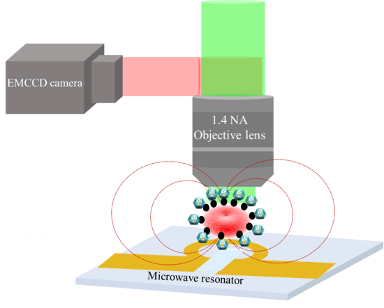
Summary of the various sub-diffraction imaging techniques applied using color centers in nanodiamonds and SiC.
Stefania Castelletto from RMIT University (Melbourne, Australia) and Alberto Boretti from Prince Mohammad Bin Fahd (Saudia Arabia) have critically reviewed the performance of the above color centers in advancing and pioneering superresolution methods based on their specific functionalities. These emerging fluorescent tags can be used as fluorescent nanoprobes because of their high absorption cross-section, low photoionization permitting to achieve the highest resolution among all fluorescent nanoprobes, and possibly extending imaging time, necessary for tracking the physical process. Their spin-dependent optical transitions can allow nanoscale imaging of magnetic fields.
In addition to having provided record resolution for STED or SMLM using as example nanodiamonds with a red emission based on a color center known as the nitrogen-vacancy (NV), novel methods based on these defects have been implemented namely spin-STED, spin-SMLM, and charge state depletion microscopy (CSD) together with its spin-CSD version. Due to the quantum light photons statistics of these color centers, other approaches (Quantum-SRM) are also investigated to achieve super-resolution based on constructing photon-correlation maps of the nanoprobes.
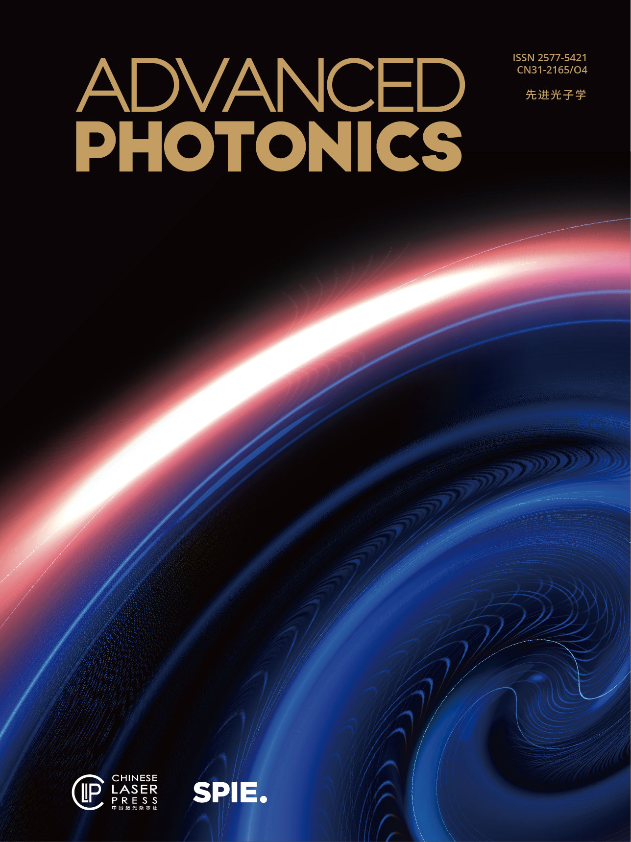
The charge and spin variant methods are originated from the photophysical properties of the NV center such as its charge state conversion from neutral to negative state, and its photoluminescence modulation depending on microwave and magnetic field excitation, making the nanocrystals tiny magnetic sensors able to produce a nanometric resolution in imaging magnetic field.
Among the most notable results is the use of NV in diamond and nanodiamonds to perform imaging localization with 30 nm and magnetic imaging with a resolution of 20-100 nm. These resolutions could be achieved with various methods such as spin-SMLM, spin-CSD, and spin-STED and their variant.
Many challenges still exist to move these nanoprobes from the research laboratory to real applications in biomedical imaging. One issue with for example NV in nanodiamond is the relatively large size of the nanocrystals (50 nm) that limits their applicability. Other color centers in SiC nanocrystals and hBN flakes can be fabricated with color centers with similar physical properties of NV in diamond but in smaller dimensions approaching few nanometers. However, for these color centers, while they can be applied in traditional SRM methods such as STED and SMLM, their application with their spin-variant method is still lacking and more research in their synthesis and performance for nano MRI is needed.
Read the open access article "Color centers in wide-bandgap semiconductors for subdiffraction imaging: a review," Advanced Photonics, 2021, 3(5): 054001