Journals >Opto-Electronic Advances
Contents


2018
Volume: 1 Issue 8
3 Article(s)
Export citation format
Contents

[in Chinese]
[in Chinese]
Opto-Electronic Advances
- Publication Date: Jan. 01, 1900
- Vol. 1, Issue 8, 1 (2018)


Original Article
Perfect electromagnetic and sound absorption via subwavelength holes array
[in Chinese], [in Chinese], [in Chinese], [in Chinese], and [in Chinese]
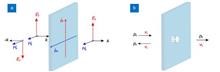
Broadband sound absorption at low frequency is notoriously difficult because the thickness of the absorber should be proportional to the working wavelength. Here we report an acoustic metasurface absorber following the recent theory developed for electromagnetics. We first show that there is an intrinsic analogy betweeBroadband sound absorption at low frequency is notoriously difficult because the thickness of the absorber should be proportional to the working wavelength. Here we report an acoustic metasurface absorber following the recent theory developed for electromagnetics. We first show that there is an intrinsic analogy between the impedance description of sound and electromagnetic metasurfaces. Subsequently, we demonstrated that the classic Salisbury and Jaumann absorbers can be realized for acoustic applications with the aid of micro-perforated plates. Finally, the concept of coherent perfect absorption is introduced to achieve ultrathin and ultra-broadband sound absorbers. We anticipate that the approach proposed here can provide helpful guidance for the design of future acoustic and electromagnetic devices..
Opto-Electronic Advances
- Publication Date: Jan. 01, 1900
- Vol. 1, Issue 8, 180013 (2018)
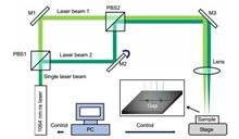
Enhancement of laser ablation via interacting spatial double-pulse effect
Rui Zhou, Shengdong Lin, Ye Ding, Huan Yang, Kenny Ong Yong Keng, and Minghui Hong
A novel spatial double-pulse laser ablation scheme is investigated to enhance the processing quality and efficiency for nanosecond laser ablation of silicon substrate. During the double-pulse laser ablation, two splitted laser beams simultaneously irradiate on silicon surface at a tunable gap. The ablation quality and A novel spatial double-pulse laser ablation scheme is investigated to enhance the processing quality and efficiency for nanosecond laser ablation of silicon substrate. During the double-pulse laser ablation, two splitted laser beams simultaneously irradiate on silicon surface at a tunable gap. The ablation quality and efficiency are evaluated by both scanning electron microscope and laser scanning confocal microscope. As tuning the gap distance, the ablation can be significantly enhanced if the spatial interaction between the two splitted laser pulses is optimized. The underlying physical mechanism for the interacting spatial double-pulse enhancement effect is attributed to the redistribution of the integrated energy field, corresponding to the temperature field. This new method has great potential applications in laser micromachining of functional devices at higher processing quality and faster speed..
Opto-Electronic Advances
- Publication Date: Jan. 01, 1900
- Vol. 1, Issue 8, 180014 (2018)
© Copyright 2018-2021 | Chinese Laser Press. All Rights Reserved 沪ICP备15018463号-20