
Ning Li, Qingyi Zhang, Yongtao Yang, Yuanjun Tang, Tao Zhang, Jiaying Shen, Yuehui Wang, Fan Zhang, Yang Zhang, Zhenping Wu. Solar-blind avalanche photodetector based on epitaxial Ga2O3/La0.8Ca0.2MnO3 pn heterojunction with ultrahigh gain[J]. Chinese Optics Letters, 2023, 21(5): 051604
- Chinese Optics Letters
- Vol. 21, Issue 5, 051604 (2023)
Abstract
1. Introduction
Significant progress has been made in the development of solar-blind photodetectors (PDs) that operate in the ultraviolet (UV) wavelength range (200–280 nm) for a variety of applications, such as secure communication, missile guidance, environmental monitoring, UV astronomy, and position navigation[1–3]. Solar-blind PDs made of wide bandgap (WBG) semiconductors with bandgap () exceeding 4.4 eV have demonstrated great potential for replacing currently available commercial photomultiplier tube (PMT) PDs, which have limitations such as being bulky, fragile, and requiring Wood’s filters to cut off the detecting wavelength[4]. To date, available WBG semiconductors include MgZnO (, alloying)[5], AlGaN (, alloying)[6], (, polymorph-dependent)[7], and diamond (, fixed)[8]. Among them, possesses several evident advantages, such as a suitable Eg for solar-blind sensing, high exciton binding energy (up to 40–50 meV at room temperature), a large breakdown electric field up to 8 MV/cm, excellent thermal, chemical, and radiation stability, plus the availability of scalable high-quality crystals and films, making it a building block for solar-blind PDs[9,10].
To date, -based solar-blind PDs have been fabricated with various device configurations, including the photoconductive[11–13], Schottky diode[14–16], heterojunction[17–19], and avalanche PD (APD)[20-23]. Compared with other types of PDs, APDs offer orders of magnitude higher responsivity and gain and are conceivably becoming the research hotspot of the field. All solid-state -based APDs allow low voltage operation and optical filter-free integration, promising more compact and robust solar-blind PDs. Through unremitting efforts, the performance metrics for reported APDs are being continually pushed in the direction of realizing high responsivity and avalanche gain. APDs work in a high reverse bias condition, so this allows avalanche multiplication of the charge carriers formed upon the UV photon impact. The photon-induced charge carriers are accelerated and undergo cascade amplifications through impact ionization with the electric field in the depletion region. APDs implemented using pn junctions are favored to form a broader depletion region. However, most reported -based APDs so far are made of n-n isotype heterojunctions, which take into account the intrinsic n-type nature of and the associated band alignments[20–22,24]. Integrating high-quality epitaxial with a p-type semiconductor layer remains a promising approach to enhance the APDs’ performance, but there are challenges associated with the integration difficulty on alleviating the defects and dislocations.
Orthorhombic perovskite manganites in the form of (where Re and Ak are rare-earth and alkaline-earth ions, respectively) have raised considerable interest for their fascinating physical properties[25,26]. In manganite-based systems, the cross coupling between different degrees of freedom (structural, charge, spin, and orbital) gives rise to rich physical phenomena, such as colossal magnetoresistance, charge/orbital ordering, and electronic phase separation[27]. Especially, when the alkaline-earth ion is a divalent ion such as , , and , manganites exhibit hole-doped p-type semiconductor characteristics with considerable large hole carrier concentrations[25]. Meanwhile, with a compatible lattice constant, perovskite manganites could be used as excellent p-type materials to form a pn junction with [28]. In this study, we construct a solar-blind APD based on epitaxial /La0.8Ca0.2MnO3 (LCMO) pn junction with ultrahigh gain and responsivity, which is approaching the benchmark of commercial PMTs. Moreover, perovskite manganites LCMO is an excellent p-type semiconductor promoting epitaxial growth of various perovskite functional oxides. The integration technology demonstrated in this work will be an important exploration in developing high-performance -based electronic and photonic devices.
Sign up for Chinese Optics Letters TOC. Get the latest issue of Chinese Optics Letters delivered right to you!Sign up now
2. Experiments
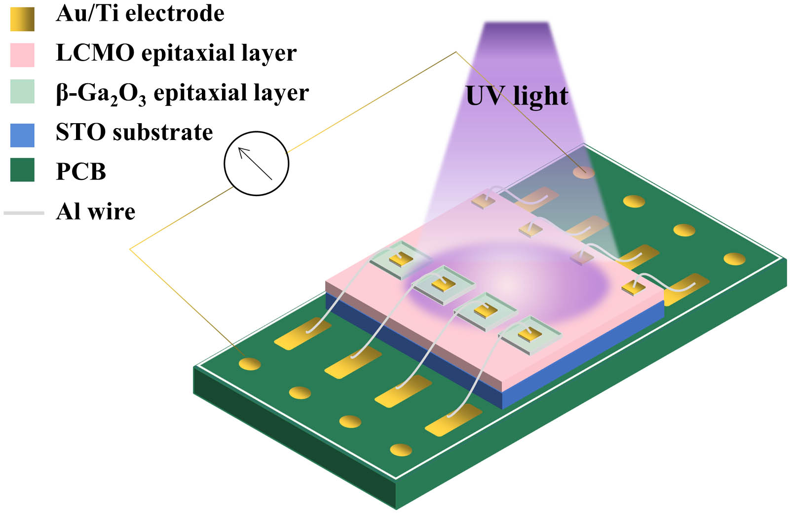
The commercial (001)-oriented (STO) single crystal () was employed as the substrate. A 100 nm thick p-type LCMO layer was deposited using the pulsed-laser deposition (PLD) technique with the following parameters: a growth temperature of 700°C, an pressure of 20 Pa, a pulse energy of , and a repetition frequency of 2 Hz. After deposition, the sample was annealed at 700°C under an pressure of for 30 min before natural cooling down. Squared patterns with an area size of were defined using a room-temperature-grown amorphous STO layer via standard photolithograhy and lift-off procedure. A 300 nm thick film was then deposited using magnetron sputtering with the following parameters: a growth temperature of 760°C, an Ar pressure of 1 Pa, and an RF power of 70 W. Then, squared Au/Ti metals were sputtered on top of both the and LCMO layers as the ohmic contact electrodes and were connected to a printed circuit board (PCB) using wire bonding. The schematic structure of the APD device is shown in Fig. 1. The crystalline quality of the sample was recorded by a Rigaku D/max2500PC X-ray diffractometer. A Hitachi U3900 UV-VIS spectrometer was used to examine the optical bandgap of the sample. A Keithley 4200 semiconductor characterization system was employed to investigate the current-voltage (I-V) characteristics. A commercial low-pressure UV lamp was employed as the 254 nm light source. The chemical bonding property was studied using a Thermo Scientific K-Alpha+ XPS system with a monochromated Al-Ka (energy of 1486.6 eV) X-ray source.
![]()
Figure 1.Schematic structure of the β-Ga2O3/LCMO pn junction APD.
3. Results
Figure 2(a) shows the X-ray diffraction (XRD) patterns of the LCMO layer and bilayer grown on STO substrates. The results indicate that the layer is of the monoclinic phase (ICSD No. 34243). In addition to the STO substrate peaks, both and LCMO exhibit obvious (100)-oriented diffraction peaks. This suggests that the LCMO/STO and heterostructures are epitaxial in nature, with the crystal lattices of the different layers aligned with each other. If we consider the lattice compatible with oxygen atom spacings between the and LCMO structures, the in-plane epitaxial relationship of the heterostructure is [001] STO, indicating a specific orientation rotation between each layer. The d spacing of the (400) plane of is determined to be 3.017 Å from the peak position, slightly larger than the bulk value of 2.971 Å. This indicates that the layer is under in-plane compressive strain due to lattice misfit. Figure 2(b) shows the cross-sectional view of the atomic-level arrangement of the heterostructure interface, which is critical for the performance and functionality of the device.
![]()
Figure 2.(a) XRD patterns of β-Ga2O3/LCMO/STO (red line) and LCMO/STO (black line); (b) atomic diagram of cross section in the (100) direction of pn junction.
We then investigated the UV photoresponse performance of the APD with a pn junction in detail. Figure 3(a) shows the I-V curves of the APD in the dark and under various intensities of 254 nm light, all of which exhibit typical rectification characteristics. As the light intensity increases from 1 to , the measured photocurrent presents an increasing trend. As shown in the inset of Fig. 3(a), the current increases as the light intensity increases, even at a high voltage of . The multiplication gain M reflects the device’s ability to amplify the photocurrent through avalanche multiplication and represents an important figure of merit (FOM) for evaluating the performance of an APD. Thus, APDs endowed with a higher multiplication gain will be more effective for amplifying the photocurrent. It is defined as follows:
![]()
Figure 3.Solar-blind photoresponse characteristics of Ga2O3/LCMO APD. (a) I-V curves (log scale) in dark and under different light illumination (1–100 µW/cm2). The inset shows the I-V curves enlarged near −37 V. (b) Reverse I-V curves in dark and under 1 µW/cm2 254 nm light intensity; the right axis shows the multiplication gain values. (c) The light intensity-dependent photocurrent and responsivity at a reverse bias of 20 V. (d) Photoresponse spectrum at a reverse bias of 30 V.
The external quantum efficiency (EQE) and linear dynamic range (LDR) are two other important FOMs for assessing the performance of the APD. The EQE is the ratio of the number of carriers produced by the PD to the number of incident photons: , where is the responsivity, is Planck’s constant, is the speed of light, is the electron charge, and is the incident light wavelength. The EQE can be used to evaluate the efficiency of a PD converting light into electrical charge. The LDR is defined as the ratio of the maximum to minimum detectable light intensity and is typically expressed in decibels (dB). An APD with a high LDR can accurately detect a wide range of light intensities, which is important in applications where the light intensity may vary over a wide range. It is calculated by , where and are the photocurrent and dark current, respectively. The , EQE, and LDR for the pn junction APD as a function of reverse bias are displayed in Figs. 4(a)–4(c). The maximum , EQE, and LDR reached 568 A/W, , and 83.3 dB, respectively. The obtained FOMs for pn junction APDs surpass those of reported -based photoconductive PDs[30,31] and rank among the best values for -based APDs[20–22,24].
![]()
Figure 4.(a) Responsivity; (b) EQE; and (c) LDR of Ga2O3/LCMO pn junction APD under 1 µW/cm2 254 nm UV light intensity as a function of reverse bias.
4. Discussion
The photoresponse performance of an APD primarily determines its energy band alignment, specifically, the barrier height (), built-in potential, and band offsets ( and )[32]. We conducted X-ray photoelectron spectroscopy (XPS) to explore the band diagrams of the pn junction. To conduct high-resolution XPS study, we prepared three samples: , , and . After calibrating the binding energy shift of the XPS spectra using the C 1s peak (284.8 eV), we applied Kraut’s method to extract the band offsets of the pn junction as follows[33]:
In LCMO, Mn exists in different valence states ( and ). is the more dominant component and exhibits a more significant peak in XPS studies. Therefore, we used the and Ga core levels (CLs) of LCMO and , respectively, for the valence band offset calculations. Furthermore, we partially extrapolate the tangent line near the low binding energy position to intersect with the horizontal extension line and determine the valence band maximum at the intersection point. From Figs. 5(a)–5(c), we can obtain the values of 1114.34 eV, 640.18 eV, and 476.71 eV for , , and , respectively. is calculated to be 2.55 eV according to Eq. (2). We performed UV-VIS absorption spectrum measurement on and LCMO films, and the obtained data were processed using the Tauc plots method to obtain versus , as shown in Figs. 5(d) and 5(e). By extrapolating Figs. 5(d) and 5(e), the of and LCMO are found to be 4.88 and 1.42 eV, respectively, which are consistent with previous studies[7,26]. By substituting these values into Eq. (3), we can determine the value of as 0.91 eV. These results are illustrated in the band alignment diagram of the heterojunction in Fig. 5(f). The pn junction exhibits a Type-I nested alignment with a large of 2.55 eV, which forms an effective barrier against hole injection in the layer, resulting in a large space charge region in the heterojunction. The formed broader depletion region increases the carrier acceleration distance and promotes intense impact ionization.
![]()
Figure 5.CL and valence band XPS energy spectrum of (a) LCMO (∼100 nm)/STO and (b) Ga2O3 (∼300 nm)/LCMO (∼100 nm)/STO; (c) CL XPS energy spectrum of Ga2O3 (∼3 nm)/LCMO (∼100 nm)/STO sample; (d) bandgap of Ga2O3 film; and (e) LCMO film determined by Tauc plots method; (f) band alignment at the Ga2O3/LCMO pn junction.
When a reverse bias is applied to a pn junction APD, migrations of holes from to LCMO and electrons from LCMO to occur simultaneously. This process is illustrated in Fig. 6. At low reverse bias, the built-in electric field in the space charge region of blocks the photogenerated carriers generated upon the 254 nm UV irradiation. As the reverse bias voltage increases, the carriers gain more kinetic energy, which allows them to overcome the electric field barrier. By increasing the reverse bias, photon-induced charge carriers are accelerated and undergo cascade amplifications through impact ionization within the broader depletion layer. Such a multiplication process allows enhanced photoresponsivity and avalanche gain[29].
![]()
Figure 6.Avalanche multiplication process of Ga2O3/LCMO APD.
5. Conclusion
In summary, the epitaxial pn junction exhibits outstanding photoelectric response characteristics in the solar-blind APD. The band alignment of the heterojunction was also studied to understand its avalanche breakdown mechanism. The nested arrangement of the band alignment results in a large valence band offset at the interface, which allows the photoexcited carriers to be accelerated by increasing the reverse bias. The designed APD incorporating epitaxial pn junction exhibits a broader depletion region, contributing to a large responsivity of 568 A/W as well as an enhanced avalanche gain of up to at a reverse bias voltage of 37.9 V. Moreover, is an emerging WBG semiconductor for various applications of power electronics and optoelectronics. Thus, the capability of epitaxially integrating with p-type semiconductor demonstrated in this work offers more opportunities to develop high-performance -based electronic and optoelectronic devices.
References
[1] X. Chen, F. Ren, S. Gu, J. Ye. Review of gallium-oxide-based solar-blind ultraviolet photodetectors. Photonics Res., 7, 381(2019).
[2] J. Chen, W. Ouyang, W. Yang, J. H. He, X. Fang. Recent progress of heterojunction ultraviolet photodetectors: materials, integrations, and applications. Adv. Funct. Mater., 30, 1909909(2020).
[3] D. Kaur, M. Kumar. A strategic review on gallium oxide based deep-ultraviolet photodetectors: recent progress and future prospects. Adv. Opt. Mater., 9, 2002160(2021).
[4] X. Zhengyuan, B. M. Sadler. Ultraviolet communications: potential and state-of-the-art. IEEE Commun. Mag., 46, 67(2008).
[5] M. M. Fan, K. W. Liu, Z. Z. Zhang, B. H. Li, X. Chen, D. X. Zhao, C. X. Shan, D. Z. Shen. High-performance solar-blind ultraviolet photodetector based on mixed-phase ZnMgO thin film. Appl. Phys. Lett., 105, 011117(2014).
[6] B. Liu, D. Chen, H. Lu, T. Tao, Z. Zhuang, Z. Shao, W. Xu, H. Ge, T. Zhi, F. Ren, J. Ye, Z. Xie, R. Zhang. Hybrid light emitters and UV solar-blind avalanche photodiodes based on III-nitride semiconductors. Adv. Mater., 32, e1904354(2020).
[7] X. Hou, Y. Zou, M. Ding, Y. Qin, Z. Zhang, X. Ma, P. Tan, S. Yu, X. Zhou, X. Zhao, G. Xu, H. Sun, S. Long. Review of polymorphous Ga2O3 materials and their solar-blind photodetector applications. J. Phys. D, 54, 043001(2021).
[8] Y.-J. Lu, C.-N. Lin, C.-X. Shan. Optoelectronic diamond: growth, properties, and photodetection applications. Adv. Opt. Mater., 6, 1800359(2018).
[9] Y. Yuan, W. Hao, W. Mu, Z. Wang, X. Chen, Q. Liu, G. Xu, C. Wang, H. Zhou, Y. Zou, X. Zhao, Z. Jia, J. Ye, J. Zhang, S. Long, X. Tao, R. Zhang, Y. Hao. Toward emerging gallium oxide semiconductors: a roadmap. Fundam. Res., 1, 697(2021).
[10] S. J. Pearton, J. Yang, P. H. Cary, F. Ren, J. Kim, M. J. Tadjer, M. A. Mastro. A review of Ga2O3 materials, processing, and devices. Appl. Phys. Rev., 5, 011301(2018).
[11] X. Hou, X. Zhao, Y. Zhang, Z. Zhang, Y. Liu, Y. Qin, P. Tan, C. Chen, S. Yu, M. Ding, G. Xu, Q. Hu, S. Long. High-performance harsh-environment-resistant GaOx solar-blind photodetectors via defect and doping engineering. Adv. Mater., 34, 2106923(2022).
[12] N. Liu, T. Zhang, L. Chen, J. Zhang, S. Hu, W. Guo, W. Zhang, J. Ye. Fast-response amorphous Ga₂O₃ solar-blind ultraviolet photodetectors tuned by a polar AlN template. IEEE Electron Device Lett., 43, 68(2022).
[13] Y. Chen, Y. Lu, M. Liao, Y. Tian, Q. Liu, C. Gao, X. Yang, C. Shan. 3D solar-blind Ga2O3 photodetector array realized via origami method. Adv. Funct. Mater., 29, 1906040(2019).
[14] B. Qiao, Z. Zhang, X. Xie, B. Li, K. Li, X. Chen, H. Zhao, K. Liu, L. Liu, D. Shen. Avalanche gain in metal-semiconductor-metal Ga2O3 solar-blind photodiodes. J. Phys. Chem. C, 123, 18516(2019).
[15] W. Y. Kong, G. A. Wu, K. Y. Wang, T. F. Zhang, Y. F. Zou, D. D. Wang, L. B. Luo. Graphene-β-Ga2O3 heterojunction for highly sensitive deep UV photodetector application. Adv. Mater., 28, 10725(2016).
[16] Y. Wang, Z. Yang, H. Li, S. Li, Y. Zhi, Z. Yan, X. Huang, X. Wei, W. Tang, Z. Wu. Ultrasensitive flexible solar-blind photodetectors based on graphene/amorphous Ga2O3 van der Waals heterojunctions. ACS Appl. Mater. Interfaces, 12, 47714(2020).
[17] Y. Wang, Y. Tang, H. Li, Z. Yang, Q. Zhang, Z. He, X. Huang, X. Wei, W. Tang, W. Huang, Z. Wu. p-GaSe/n-Ga2O3 van der Waals heterostructure photodetector at solar-blind wavelengths with ultrahigh responsivity and detectivity. ACS Photonics, 8, 2256(2021).
[18] Z. Wu, L. Jiao, X. Wang, D. Guo, W. Li, L. Li, F. Huang, W. Tang. A self-powered deep-ultraviolet photodetector based on an epitaxial Ga2O3/Ga:ZnO heterojunction. J. Mater. Chem. C, 5, 8688(2017).
[19] Y. Wang, W. Cui, J. Yu, Y. Zhi, H. Li, Z. Y. Hu, X. Sang, E. J. Guo, W. Tang, Z. Wu. One-step growth of amorphous/crystalline Ga2O3 phase junctions for high-performance solar-blind photodetection. ACS Appl. Mater. Interfaces, 11, 45922(2019).
[20] B. Zhao, F. Wang, H. Chen, Y. Wang, M. Jiang, X. Fang, D. Zhao. Solar-blind avalanche photodetector based on single ZnO–Ga2O3 core–shell microwire. Nano Lett., 15, 3988(2015).
[21] Y. Wang, H. Li, J. Cao, J. Shen, Q. Zhang, Y. Yang, Z. Dong, T. Zhou, Y. Zhang, W. Tang, Z. Wu. Ultrahigh gain solar blind avalanche photodetector using an amorphous Ga2O3-based heterojunction. ACS Nano, 15, 16654(2021).
[22] X. Chen, Y. Xu, D. Zhou, S. Yang, F. F. Ren, H. Lu, K. Tang, S. Gu, R. Zhang, Y. Zheng, J. Ye. Solar-blind photodetector with high avalanche gains and bias-tunable detecting functionality based on metastable phase alpha-Ga2O3/ZnO isotype heterostructures. ACS Appl. Mater. Interfaces, 9, 36997(2017).
[23] Q. Zhang, N. Li, T. Zhang, D. Dong, Y. Yang, Y. Wang, Z. Dong, J. Shen, T. Zhou, Y. Liang, W. Tang, Z. Wu, Y. Zhang, J. Hao. Enhanced gain and detectivity of unipolar barrier solar blind avalanche photodetector via lattice and band engineering. Nat. Commun., 14, 418(2023).
[24] W. E. Mahmoud. Solar blind avalanche photodetector based on the cation exchange growth of β-Ga2O3/SnO2 bilayer heterostructure thin film. Sol. Energy Mater. Sol. Cells, 152, 65(2016).
[25] M. B. Salamon, M. Jaime. The physics of manganites: structure and transport. Rev. Mod. Phys., 73, 583(2001).
[26] J. M. D. Coey, M. Viret, S. von Molnár. Mixed-valence manganites. Adv. Phys., 48, 167(1999).
[27] Z. Liao, M. Huijben, Z. Zhong, N. Gauquelin, S. Macke, R. J. Green, S. Van Aert, J. Verbeeck, G. Van Tendeloo, K. Held, G. A. Sawatzky, G. Koster, G. Rijnders. Controlled lateral anisotropy in correlated manganite heterostructures by interface-engineered oxygen octahedral coupling. Nat. Mater., 15, 425(2016).
[28] J. Yu, Y. Wang, H. Li, Y. Huang, W. Tang, Z. Wu. Tailoring the solar-blind photoresponse characteristics of β-Ga2O3 epitaxial films through lattice mismatch and crystal orientation. J. Phys. D, 53, 24LT01(2020).
[29] S. O. Kasap. Optoelectronics and Photonics: Principles and Practices(2012).
[30] M.-Q. Li, N. Yang, G.-G. Wang, H.-Y. Zhang, J.-C. Han. Highly preferred orientation of Ga2O3 films sputtered on SiC substrates for deep UV photodetector application. Appl. Surf. Sci., 471, 694(2019).
[31] G. C. Hu, C. X. Shan, N. Zhang, M. M. Jiang, S. P. Wang, D. Z. Shen. High gain Ga2O3 solar-blind photodetectors realized via a carrier multiplication process. Opt. Express, 23, 13554(2015).
[32] G. Greczynski, L. Hultman. X-ray photoelectron spectroscopy: towards reliable binding energy referencing. Prog. Mater Sci., 107, 100591(2020).
[33] Z. Liu, J. Yu, P. Li, X. Wang, Y. Zhi, X. Chu, X. Wang, H. Li, Z. Wu, W. Tang. Band alignments of β-Ga2O3 with MgO, Al2O3 and MgAl2O4 measured by X-ray photoelectron spectroscopy. J. Phys. D, 52, 295104(2019).

Set citation alerts for the article
Please enter your email address
© Copyright 2018-2021 | Chinese Laser Press. All Rights Reserved 沪ICP备15018463号-20