
Yunlong Zhu, Zhuoran Li, Xu Lu, Yonggui Yuan, Jun Yang. White light interferometry with spectral-temporal demodulation for large-range thickness measurement[J]. Chinese Optics Letters, 2022, 20(9): 091201
- Chinese Optics Letters
- Vol. 20, Issue 9, 091201 (2022)
Abstract
1. Introduction
Thin films play important roles in the fields of semiconductors, optoelectronics, integrated optics, etc. Following the increasing demand on thin film quality[
The measurement of film thickness using WLI can be realized through time-domain detection[
Since the Fourier transform of the time-domain interferometric signal is equivalent to the spectrum when the numerical aperture (NA) is approximately equal to zero[
Sign up for Chinese Optics Letters TOC. Get the latest issue of Chinese Optics Letters delivered right to you!Sign up now
In this paper, we propose a spectral-temporal demodulation method to realize high-precision thickness measurement in a large range of thicknesses. The theoretical full-range precision and lower limit of thickness are determined by the spectral demodulation method, and the theoretical upper limit of thickness is determined by the scanning range of the optical delay line. A home-made fiber-optic scanning WLI with gradient-index (GRIN) lens probe[
2. Principle
In this paper, we use scanning WLI to realize thickness measurement of transparent coating or substrate-free film with a large thickness range. A home-made WLI system[
The reflected light field from the reflecting surface and the film under test can be expressed as
For coatings (without reflection from the backside of the substrate) and substrate-free films, the refractive index of the film under test is set to be , and the refractive index of the substrate (or air for substrate-free films) is set to be . We define as the thickness of film; thus the reflectance of the coating can be expressed as follows:
Also, the reflectance and the transmittance of the probe are expressed as follows:
In the scanning WLI, the light is divided into two beams after passing through the coupler. After passing through the optical delay line, the two beams interfere with each other, and the total light field is
It can be seen from Eqs. (11)–(14) that due to the low coherence of the broad-spectrum light source, there are three peaks in the interferometric signal (around , , , respectively). By demodulating the distance between these peaks, we can obtain , which means the profile of the thin film surface can be obtained with two-dimensional detection. Since only single-point detection is applied in our experiments, the demodulation of is not discussed in this paper.
This scanning process is actually equivalent to FTIR measurement of . The time-domain interference signal is the Fourier transform of the spectral signal, and vice versa. In the time domain, we can easily separate the interferometric signal around the central peak () to obtain the spectrum :
This step has the same intention of applying a “spectral carrier” described in Ref. [3], yet we take only one Fourier transform instead of two, since the time-domain signal is directly taken.
Without film under test, the reflectance spectrum of the reflecting surface in probe to be measured is
When testing a reference surface with known reflectance , the reference spectral can be obtained:
According to Eqs. (15)–(18), the reflectance spectrum can be obtained:
The film thickness can be obtained by fitting to the theoretical curve described by Eqs. (3)–(6). The sum of squared errors is described as
The Levenberg–Marquardt (LM) algorithm[
However, for a film with a large thickness, the OPD between the front and back is usually much larger than the coherence length of the white light source. Therefore, the rough value of film thickness can be obtained in the time-domain interferometric signal by the envelope method[
We should also pay attention to another issue concerning the fitting process. oscillates with higher frequency in the spectral domain while dealing with larger thicknesses. In this case, phase error may occur in the spectral signal[
Theoretically, the obtained phase can be used for the fitting process. However, is a wrapped phase signal, which means the phase ambiguity of the integer multiple of exists. Although can be unwrapped with the proper algorithm, which avoids the phase jump around 0 and , the integer multiple of may still exist between measured and theoretical values of . For this reason, additional preprocessing is needed before the fitting of , which will increase the algorithmic complexity. Besides, incorrect unwrapped values of and the deviation of at few points tend to cause relatively large error when a direct fitting of unwrapped is carried out. In order to get more reliable fitting results with a simpler process, we define signal as
contains the phase information of , and the sudden jumps caused by phase wrapping in are also avoided. Although the cosine function may change the frequency distribution of noise, experimental results show that the influence is negligible. So, for the simplicity and reliability of the thickness demodulation process, we fit instead of while measuring large thickness.
3. Experimental Results
In the experiments, the center wavelength of the white light source is 1310 nm, and the full width at half-maximum of the spectrum is about 70 nm. In order to verify the reliability of the proposed method, a 500 nm coating on the Si substrate and a 68 µm substrate-free film were selected for thickness measurement. The back surface of the Si substrate for coating is a highly scattering surface, so the reflection can be ignored although Si is transparent to the 1310 nm light source. The optical thickness of the coating is smaller than the coherence length of the light source, so the peaks caused by different surfaces of the thin film overlap with each other. On the contrary, the optical thickness of the Si film is greater than the coherence length, so the peaks caused by different surfaces of thin film can be distinguished. To measure the thickness and uniformity of the films, classical five-point measurement was carried out for each film, and five repeated measurements were performed at each point.
According to Eq. (19), , , , and need to be known to calculate . In our experiments, is measured using the film under test ( coating or substrate-free Si film), is measured without any film facing the probe, is measured using a bare Si wafer with a polished front surface and highly scattering back surface, and is calculated according to the refractive index of Si. Since the fluctuation of ambient temperature may have an influence on the measurements, the measurements are preferred to be carried out with the minimum time interval.
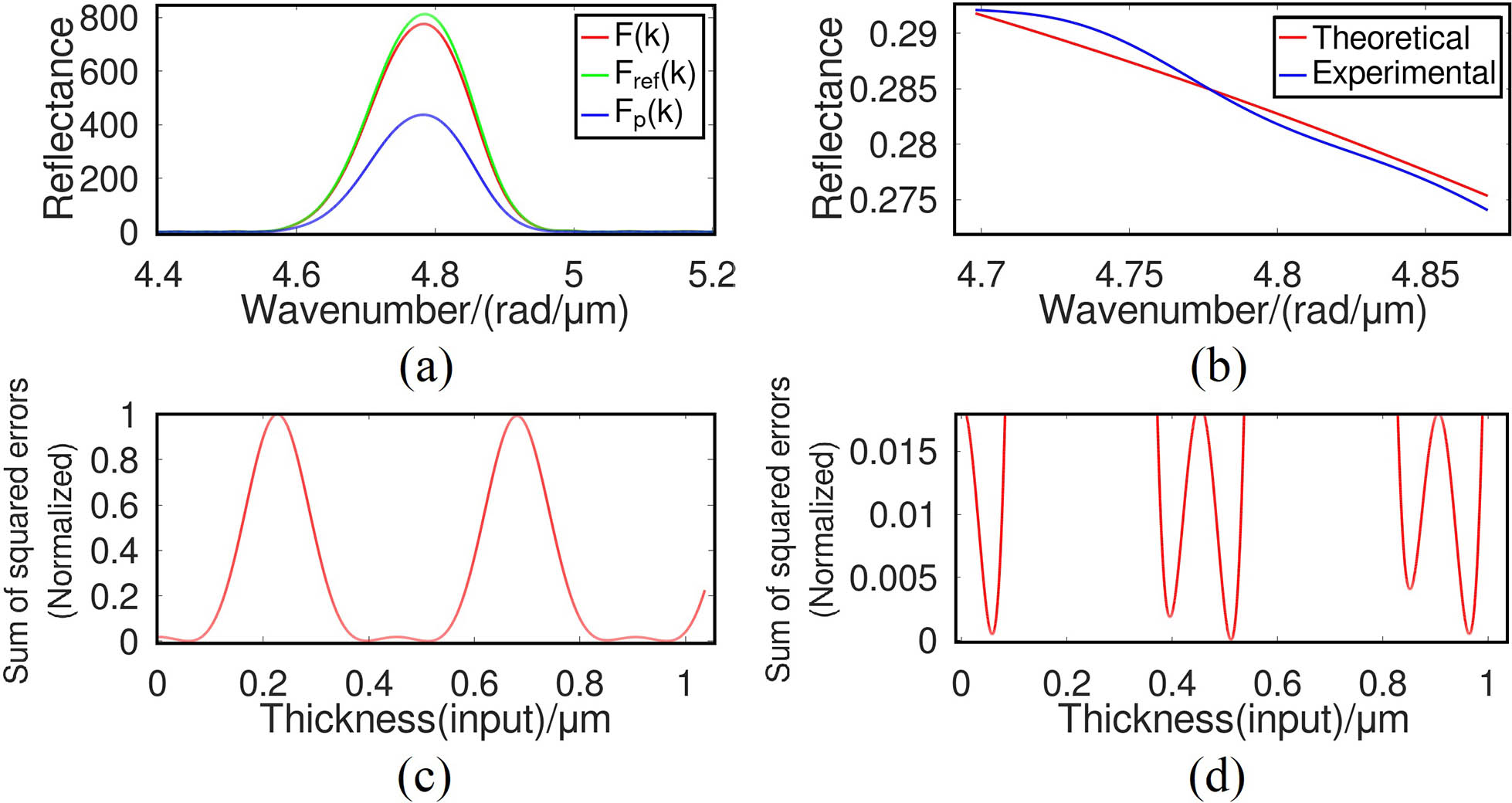
For the measurement of 500 nm coating, , , and for one of the measurements are shown in Fig. 1(a). Least squares fitting is carried out directly with the reflectance spectrum . The initial value for the LM algorithm is directly set to be 500 nm. The experimental and theoretical curves of are shown in Fig. 1(b), where the value of thickness for the calculation of the theoretical curve is the result given by the LM algorithm. The complete measurement results are shown in Table 1. Among the five points, the maximum single-point standard deviation is 0.70 nm. It can also be calculated that the average thickness of the film is 509.35 nm, and the standard deviation between the five points is 2.57 nm.
| Number of Measurement | Point A | Point B | Point C | Point D | Point E |
|---|---|---|---|---|---|
| 1st | 508.18 | 511.34 | 506.86 | 508.84 | 513.53 |
| 2nd | 508.67 | 511.09 | 505.66 | 508.62 | 512.71 |
| 3rd | 507.31 | 511.60 | 506.88 | 508.98 | 512.03 |
| 4th | 507.65 | 511.36 | 506.52 | 508.26 | 512.81 |
| 5th | 508.00 | 511.53 | 506.03 | 507.23 | 512.07 |
| Average | 507.96 | 511.38 | 506.39 | 508.39 | 512.63 |
| Standard deviation | 0.52 | 0.20 | 0.53 | 0.70 | 0.62 |
Table 1. Measurement Results for 500 nm
![]()
Figure 1.Experimental results for a single measurement of 500 nm SiO2 coating. (a) Reflectance spectrum F(k), Fref(k), and Fp(k). (b) Comparison of measured reflectance R(k) and theoretical model. (c) Normalized sum of squared errors for reflectance fitting between the experimental result and theoretical model at different values of input thickness. (d) Detailed view of (c) showing the minimum sum of squared errors.
To test the correctness of the fitting process, the sums of squared errors with ranging from 0 to 1000 nm are plotted in Fig. 1(c), while Fig. 1(d) is a detailed view showing more clearly the points of local minima. It can be seen that the minimum around 509.35 nm is truly the minimum among all the minima in this range. Besides, the nearest local minimum is about 100 nm away, so the value of 500 nm given by the manufacturer works well as the initial value for the LM algorithm.
For the measurement of 68 µm Si film, , (), and for one of the measurements are shown in Fig. 2(a). Since the thickness is relatively large, least squares fitting is carried out with described by Eq. (24). To get the proper initial values for the LM algorithm, the traditional envelope method is applied to give the values of , as shown by Table 1. For 68 µm Si film and 1310 nm light source, in Eq. (21) is estimated to be 0.18 µm. The values of in Eq. (22) are then taken as the initial values for the LM algorithm. As discussed in Section 2, seven results of thickness measurements are thus given for each measurement, and the final result is chosen to be the one with the minimum sum of squared errors.
![]()
Figure 2.Experimental results for a single measurement of 68 µm Si film. (a) Reflectance spectrum F(k), Fref(k), and Fp(k). (b) Comparison of measured reflectance R(k) and theoretical model. (c) Normalized sum of squared errors for reflectance fitting between the experimental result and theoretical model at different values of input thickness. (d) Detailed view of (c) showing the minimum sum of squared errors.
The experimental and theoretical curves of are shown in Fig. 2(b), where the value of thickness for the calculation of the theoretical curve is the final result given by the LM algorithm. The complete measurement results given by envelope method and the proposed method are shown in Tables 2 and 3, respectively. Among the five points, the maximum single-point standard deviation is 1.2 nm for the proposed method, while this value is 26 nm for the envelope method. By comparing the values of standard deviation in Tables 2 and 3, we can see that the repeatability has improved for about 30 times using the proposed method. From Table 3, it can also be calculated that the average thickness of the film is 68.45 µm, and the standard deviation between the five points is 0.13 µm.
| Number of Measurement | Point A | Point B | Point C | Point D | Point E |
|---|---|---|---|---|---|
| 1st | 68,613.59 | 68,348.37 | 68,394.21 | 68,299.25 | 68,554.65 |
| 2nd | 68,646.33 | 68,345.09 | 68,364.74 | 68,243.59 | 68,528.46 |
| 3rd | 68,613.59 | 68,322.17 | 68,387.66 | 68,282.88 | 68,557.92 |
| 4th | 68,643.06 | 68,341.82 | 68,404.03 | 68,276.33 | 68,535.00 |
| 5th | 68,597.22 | 68,358.19 | 68,390.93 | 68,295.98 | 68,593.94 |
| Average | 68,622.76 | 68,343.13 | 68,388.31 | 68,279.61 | 68,554.00 |
| Standard deviation | 21 | 13 | 15 | 22 | 26 |
Table 2. Measurement Results for 68 µm Si Film Using Envelope Method (nm)
| Number of Measurement | Point A | Point B | Point C | Point D | Point E |
|---|---|---|---|---|---|
| 1st | 68,628.97 | 68,358.91 | 68,387.23 | 68,330.20 | 68,563.33 |
| 2nd | 68,628.64 | 68,358.97 | 68,387.58 | 68,331.68 | 68,563.89 |
| 3rd | 68,629.01 | 68,359.5 | 68,388.33 | 68,332.76 | 68,564.37 |
| 4th | 68,628.80 | 68,359.38 | 68,388.35 | 68,332.86 | 68,564.22 |
| 5th | 68,629.03 | 68,359.58 | 68,388.68 | 68,333.17 | 68,564.56 |
| Average | 68,628.89 | 68,359.27 | 68,388.04 | 68,332.13 | 68,564.07 |
| Standard deviation | 0.17 | 0.31 | 0.60 | 1.2 | 0.48 |
Table 3. Measurement Results for 68 µm Si Film Using the Proposed Method (nm)
The sums of squared errors with ranging from 67.8 µm to 69.0 µm are plotted in Fig. 2(c), while Fig. 2(d) is a detailed view showing more clearly the points of local minima near 68.45 µm. It can be seen that the minimum around 68.45 µm is truly the minimum among all the minima in this range, and the intervals between the minima are around 177 nm, which is the value of that we derived. Obviously, 68 µm cannot be taken directly as the initial value for the LM algorithm, which will lead to an output of the local minimum around 68 µm, with an error of about .
The measurement uncertainty can be divided into repeatability uncertainty , nominal laser wavelength uncertainty , temperature change uncertainty , and film installation uncertainty (see Table 4). The expanded uncertainty of film thickness measurement is 0.63 nm for the 500 nm coating using the proposed method, 23 nm for 68 µm Si film using the envelope method, and 1.2 nm for 68 µm Si film using the proposed method. It can be seen that the expanded uncertainty is below 2 nm for either film using the proposed method. The expanded uncertainty is much smaller than the difference between neighboring minima shown in Figs. 1(d) and 2(d), which proves the reliability of the proposed method.
| Uncertainty Component | Source | Uncertainty Contribution |
|---|---|---|
| u(lH) | Measurement results | 0.31 nm (see Table |
| 11.63 nm (see Table | ||
| 0.54 nm (see Table | ||
| u(lf) | Nominal wavelength | |
| u(lT) | Temperature change | |
| u(ls) | Film installation |
Table 4. Summary of Measurement Uncertainty Components
4. Conclusions
Based on scanning WLI, a spectral-temporal demodulation scheme is proposed. Half of the distance between peaks (if separable) around (or ) is taken as the rough value of optical thickness of the thin film, and the Fourier transform of the central peak (around ) in the interferometric signal is analyzed to give the precise value of thickness. The proposed method is not only suitable for coatings, but also suitable for substrate-free films. We take a coating () on a Si substrate and a substrate-free Si film () as samples to test the proposed method. By comparing the errors of least square fitting, it is proved experimentally that the outputs converge to the point of minimum error. For the coating and the substrate-free Si film, the results of thickness given by the five-point method are 509.35 nm and 68.45 µm, respectively, while the maximum values of single-point repeatability are 0.70 nm and 1.22 nm, respectively. Compared with the traditional envelope method, the single-point repeatability for the Si film is about 30 times better. We believe the proposed method can be applied for a larger range of thickness, since theoretically the upper limit of thickness is only limited by the optical delay line, while constantly high precision is maintained in the full range. Besides, by applying a collimated beam and two-dimensional detector, our method can be easily extended to carry out simultaneous measurement of surface profile and film thickness.
References
[1] X. Tian, W. Zhou, K. Ren, C. Zhang, X. Liu, G. Xue, J. Duan, X. Cai, X. Hu, Y. Gong, Z. Xie, S. Zhu. Effect of dimension variation for second-harmonic generation in lithium niobate on insulator waveguide. Chin. Opt. Lett., 19, 060015(2021).
[2] . ME-L Mueller matrix ellipsometer.
[3] Y. S. Ghim, S. W. Kim. Spectrally resolved white-light interferometry for 3D inspection of a thin-film layer structure. Appl. Opt., 48, 799(2009).
[4] Y. Yang, H. Yan, S. Li, F. Yang, W. Jin. Estimation of gyro bias drift due to distributed polarization cross coupling in the fiber coil. Opt. Express, 27, 10247(2019).
[5] H. Yoshino, A. Abbas, P. M. Kaminski, R. Smith, J. M. Walls, D. Mansfield. Measurement of thin film interfacial surface roughness by coherence scanning interferometry. J. Appl. Phys., 121, 105303(2017).
[6] H. Yoshino, R. Smith, J. M. Walls, D. Mansfield. The development of thin film metrology by coherence scanning interferometry. Proc. SPIE, 9749, 97490P(2016).
[7] H. Yoshino, J. M. Walls, R. Smith. Interfacial surface roughness determination by coherence scanning interferometry using noise compensation. Appl. Opt., 56, 4757(2017).
[8] H. Yoshino, P. M. Kaminski, R. Smith, J. M. Walls, D. Mansfield. Refractive index determination by coherence scanning interferometry. Appl. Opt., 55, 4253(2016).
[9] M. F. Fay, T. Dresel. Applications of model-based transparent surface films analysis using coherence-scanning interferometry. Opt. Eng., 56, 111709(2017).
[10] Y. S. Ghim, S. W. Kim. Fast, precise, tomographic measurements of thin films. Appl. Phys. Lett., 91, 091903(2007).
[11] Y. S. Ghim, H. G. Rhee, H. S. Yang, Y. W. Lee. Thin-film thickness profile measurement using a Mirau-type low-coherence interferometer. Meas. Sci. Technol., 24, 075002(2013).
[12] K. Xue, J. Wang, Y. Zhao, Z. Xiao. Measurement of glass thickness and refractive index based on spectral interference technology. Appl. Opt., 60, 7983(2021).
[13] Y. Du, H. Yan, Y. Wu, X. Yao, Y. Nie, B. Shi. Non-contact thickness measurement for ultra-thin metal foils with differential white light interferometry. Chin. Opt. Lett., 2, 701(2004).
[14] P. J. de Groot, X. C. de Lega, M. F. Fay. Transparent film profiling and analysis by interference microscopy. Proc. SPIE, 7064, 70640I(2008).
[15] S. W. Kim, G. H. Kim. Thickness-profile measurement of transparent thin-film layers by white-light scanning interferometry. Appl. Opt., 38, 5968(1999).
[16] X. Lu, Y. Yuan, C. Ma, H. Zhu, Y. Zhu, Z. Yu, X. Zhang, F. Jiang, J. Zhang, H. Li, J. Yang, L. Yuan. Self-calibrated absolute thickness measurement of opaque specimen based on differential white light interferometry. IEEE Trans. Instrum. Meas., 69, 2507(2020).
[17] K. Madsen, H. B. Nielsen, O. Tingleff. Methods for non-linear least squares problems(2004).
[18] S. S. C. Chim, G. S. Kino. Three-dimensional image realization in interference microscopy. Appl. Opt., 31, 2550(1992).
[19] P. Hlubina, D. Ciprian, J. Luňáňek, M. Lesňák. Dispersive white-light spectral interferometry with absolute phase retrieval to measure thin film. Opt. Express, 14, 7678(2006).

Set citation alerts for the article
Please enter your email address
© Copyright 2018-2021 | Chinese Laser Press. All Rights Reserved 沪ICP备15018463号-20