
Gongqing Li, Xiaofeng Duan, Weifang Yuan, Yongqing Huang, Kai Liu, Xiaomin Ren. Quasi-resonant cavity enhanced photodetector with a subwavelength grating[J]. Chinese Optics Letters, 2022, 20(3): 031301
- Chinese Optics Letters
- Vol. 20, Issue 3, 031301 (2022)
Abstract
1. Introduction
High speed[
In order to narrow the linewidth of the photodetector, we either filter the incident light by using an external filter or integrate the filtering cavity[
With the rise of the planar dielectric materials subwavelength grating (SWG)[
Sign up for Chinese Optics Letters TOC. Get the latest issue of Chinese Optics Letters delivered right to you!Sign up now
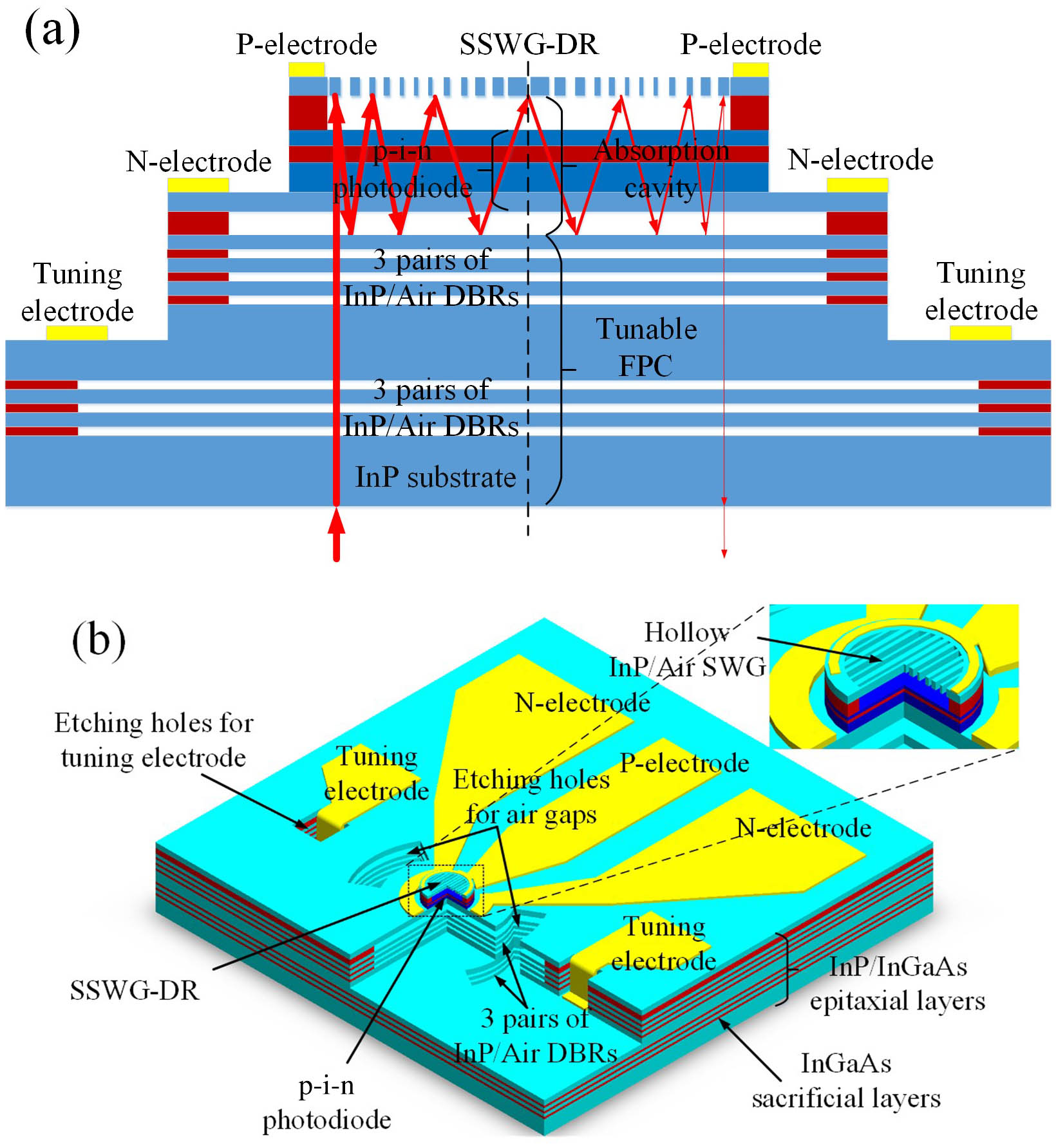
In this paper, we proposed a new decoupling method, a tunable wavelength-selective quasi-RCE-PD (QRCE-PD) based on high-contrast SWG, which is composed of InP/InGaAs materials and operates at a 1550 nm long wavelength, as shown in Fig. 1. This photodetector contains a tunable F-P filtering cavity (FPC)[
![]()
Figure 1.(a) Schematic structure and (b) schematic layout of the QRCE-PD.
2. Structure Design of QRCE-PD
For the design of the FPC, it is necessary to achieve narrow linewidth and high reflectivity at oblique incidence. The FPCs we designed are made of two distributed Bragg reflector (DBR) mirrors. The DBR mirror contains three pairs of InP/air quarter-wave stacks[
![]()
Figure 2.Reflectivity of the FPC as a function of wavelength at normal incidence (black solid line) and as a function of incident angle at the 1550 nm wavelength (red dash dot line).
For the built-in photodiode, in order to pursue a higher frequency response speed, we temporarily ignore the quantum efficiency and adopt the absorption layer thickness of only 400 nm. The layer structures used in this paper are given in Table 1. At bias, the 3 dB bandwidth of the device can reach 33.5 GHz.
| Name | Material | Doping ( | Thickness (nm) |
|---|---|---|---|
| P layer | InGaAsP | 3 × 10¹⁸ | 300 |
| Absorption layer | InGaAs | 1 × 10¹⁵ | 400 |
| Spacing layer | InGaAsP | 2 × 10¹⁵ | 1500 |
| N layer | InP | 3 × 10¹⁸ | 300 |
Table 1. Layer Structure of the Embedded p-i-n Photodiode
With respect to designing a functional SWG optical element, it is a common way to arrange grating bars or blocks with appropriate phase and diffraction efficiency to form a specific phase profile. Herein, a grating reflector with 3° deflection angle is designed and simulated by using COMSOL Multiphysics, whose reflectivity is 97%, as shown in Fig. 3(a). The structure parameters of this grating are shown in Fig. 3(b), and its thickness is fixed at 0.5 µm. Then, we mirrored this grating horizontally to form the SSWG-DR. The SSWG-DR has an inclined-ridge reflection phase plane, which makes it equivalent to an inclined-ridge reflector.
![]()
Figure 3.(a) Electric field intensity distribution and (b) structure parameters of the SWG reflector.
The design of our QRCE-PD is based on InP/InGaAs materials for long wavelength devices and uses an InP/air gap structure and hollow InP/air grating structure. The main challenge in the fabrication of our device is the selective etching of the air gaps and the hollow InP/air SWG. The hollow grating structure was realized many times by the research team of Chang-Hasnain[
3. Theoretical Model of QRCE-PD
The FPC, combined with the SSWG-DR, constitutes an inclined-ridge resonant cavity. Then, the p-i-n photodiode is embedded in it to form the QRCE-PD. In Ref. [25], the authors demonstrated that the inclined-ridge cavity is a multi-region F-P resonant cavity. QRCE-PD adopts this inclined-ridge resonant cavity structure but uses FPC instead of a bottom mirror. Figure 4(a) shows the equivalent inclined-ridge cavity structure of the QRCE-PD. By using the same method as in Ref. [25], QRCE-PD can be equivalent to a multi-region F-P cavity by multiple mutual mirroring. Figure 4(b) depicts the mirroring schematic diagram of region 1, in which the actual and equivalent optical paths are both shown, and an equivalent F-P cavity is clearly presented. The equivalent F-P cavities of other regions can also be presented in the same way.
![]()
Figure 4.(a) Equivalent inclined-ridge cavity structure of the QRCE-PD and (b) schematic diagram of forming region 1 by multiple mutual mirroring.
Figure 5 shows the equivalent multi-region F-P cavity structure of the QRCE-PD. The conclusions from Ref. [25] indicate that the optical path and width of each region are determined by the cavity length and deflection angle . Therefore, the number of resonant regions contained in a QRCE-PD depends on its and . Of course, the size and material of the embedded p-i-n photodiode also affect the optical structure within the cavity, thus affecting the distribution of resonant regions. Here, the cavity parameters of our designed QRCE-PD are also shown in Fig. 4(a). Its effective cavity length is 10.65 µm.
![]()
Figure 5.Equivalent multi-region F-P cavity structure of the QRCE-PD, which forms a multi-region RCE-PDs structure together with a built-in photodetector.
In any region of QRCE-PD, a photodetector, which is placed in an F-P cavity, is a typical RCE-PD. For a conventional RCE-PD, as employed from Ref. [10], under the assumption that all of the photo-generated carriers contribute to the detector current, the quantum efficiency could be expressed as
Fortunately and coincidentally, in the equivalent multi-region F-P cavity of the QRCE-PD, the ideal reflectivity of the FPC at the operating wavelength is zero, and the incident light will pass through the absorption layer several times when in any region. In region , the incident light will propagate through the absorption layer times, which means that the -thick absorber acts like a -thick absorber. So, the quantum efficiency in region is
The total quantum efficiency of the QRCE-PD should be the weighted average of the quantum efficiency of each region,
4. Simulation Results and Discussions
We simulated the spectral response of the QRCE-PD mentioned above by using the wave optics mode of COMSOL Multiphysics, which is based on the finite element method (FEM). In Fig. 6(a), the normalized electric field intensity distribution is shown, and the regions of our designed QRCE-PD are also identified. We know that the electric field intensity in the FPC is much stronger than that in the absorption cavity, which is consistent with the actual situation, because, in the absorption cavity, the incident light is absorbed in large quantities, while in the FPC the incident light is resonated and filtered.
![]()
Figure 6.(a) Normalized electric field intensity distribution and region distribution of the QRCE-PD. (b) Simulated spectral response of QRCE-PD, conventional RCE-PD, and p-i-n photodetector.
Under the assumption that all of the photo-generated carriers contribute to the detector current, the spectral responses of a p-i-n photodetector, an RCE-PD, and our QRCE-PD are simulated and shown in Fig. 6(b). For comparison, all three devices use the same active photodiode, which is mentioned above. The quantum efficiency of the p-i-n photodetector is only 18.9%. The peak value of the RCE-PD is near unity, but its spectral linewidth at full width at half-maximum (FWHM) is 15.9 nm. As expected, the QRCE-PD not only achieves a quantum efficiency of 93.2%, but also has the same linewidth (0.12 nm) as the FPC. In Table 2, we list the theoretical parameters of each region derived from Ref. [27] and Eq. (3), such as width, , and . Then, we can obtain the theoretical total quantum efficiency according to Eq. (4). It is 95.0%, which is higher than the actual total quantum efficiency. By comparing the simulation results to the theoretical values, we consider that the main factors that affect the quantum efficiency are the leakage of light incident from the SSWG-DR and the FPC.
| Region | Width (μm) | ||
|---|---|---|---|
| 1 | 1.12 | 0.067 | 0.663 |
| 2 | 2.23 | 0.134 | 0.887 |
| 3 | 3.33 | 0.201 | 0.962 |
| 4 | 4.43 | 0.267 | 0.987 |
| 5 | 5.51 | 0.332 | 0.996 |
| Total width | 16.62 | Total | 0.950 |
Table 2. Theoretical Parameters of Each Absorption Region
However, the peak wavelength of QRCE-PD is not 1550 nm, but shifts to 1548.45 nm unexpectedly. We consider that this offset is caused by the layer structure of the inserted photodiode, which changes the reflectivity of the top mirror of the FPC and leads to the offset of the resonant filtering center of the FPC. But, the offset can be eliminated by adjusting the reflectivity of the bottom mirror of FPC or by tuning the equivalent cavity length of the FPC. Changing the reflectivity of the bottom mirror needs to redesign the DBR; instead, adjusting the refractive index of the cavity layer of the FPC can change the equivalent cavity length to tune the peak wavelength. Under the assumption that the refractive index tuning is not limited, the QRCE-PD can obtain a wavelength-tuning range of 28 nm (1536–1564 nm) on the premise that the quantum efficiency is higher than 80%, as shown in Fig. 7. The wide wavelength-tuning ability proves that the interpretation of the offset is reasonable. The distribution of the peak wavelengths does not conform to the spectral response envelope of the RCE-PD, which indicates that high quantum efficiency is not the result of the RCE effect, but relies on the multiple-pass absorption enhanced effect. That is why our device is named the QRCE-PD.
![]()
Figure 7.Spectral response of QRCE-PD when tuning the refractive index of the cavity layer of the FPC.
These results also verify that the FPC and the absorption cavity are decoupled and relatively independent. The FPC selects the wavelength, narrows the linewidth, and is tunable by carrier injection or thermal tuning. For the coupling of the incident light, the narrow linewidth also limits the incident angle variation. From Fig. 2, we know that the coupling efficiency will decrease dramatically when incident angle is larger than about 0.5°. Referring to previous experimental work on a tunable FPC[
The frequency response performance of the p-i-n photodetector used in this paper is simulated by Silvaco ATLAS software. The mesa diameter of this device is 32 µm. The result is shown in Fig. 8, where the 3 dB bandwidth is 33.5 GHz under a reverse bias of 3 V. The bandwidth is mainly limited by the resistance-capacity time constant. Since the spectral absorption and photoelectric conversion of semiconductor devices are two relatively independent physical mechanisms, and there is currently no method to fully simulate the QRCE-PD device, we believe that it is reasonable to consider the optical response and frequency response of QRCE-PD separately. Therefore, in the future, the light detection part in QRCE-PD can be replaced by devices with higher response speed, such as the uni-traveling carrier photodetector.
![]()
Figure 8.Frequency response of the embedded p-i-n photodiode at -3 V bias.
In Table 3, for comparing the spectral response with our QRCE-PD, we list some performance parameters of several different long wavelength devices from references, such as quantum efficiency, spectral linewidth, and wavelength-tuning range. From this table, the device with the RCE structure[
| Taper cavity[ | Multi-cavities RCE[ | ||||
|---|---|---|---|---|---|
| Absorber thickness (nm) | 300 | 300 | 350 | 400 | |
| Linewidth (nm) | Theoretical | – | – | 0.5 | 0.12 |
| Experimental | 0.6 | 0.75 | – | ||
| Tuning range (nm) | Theoretical | – | – | – | 28 |
| Experimental | – | 10.2 | – | – | |
| Quantum efficiency | Theoretical | – | – | 80% | 93.2% |
| Experimental | 59% | 70% | 70% | – | |
Table 3. Performance Parameters of Different Long Wavelength Devices
5. Conclusion
In conclusion, we have proposed a tunable, high speed, high quantum efficiency, and ultra-narrow linewidth QRCE-PD with SWG, which can be equivalent to multi-region RCE-PDs by multiple mutual mirroring. The QRCE-PD structure is a new type of photodetector structure, whose most significant advantage is that it can greatly relieve the mutual restriction among quantum efficiency, response speed, and spectral linewidth. This structure can not only be applied to the DWDM system, but also provides a reference for the design of photodetectors with similar performance requirements in other optical fields.
References
[1] A. Beling, J. C. Campbell. InP-based high-speed photodetectors. J. Light. Technol., 27, 343(2009).
[2] J. Chen, Z. Zhou. Ultranarrow band and high-quantum-efficiency photo response of Ge-on-Si photodetectors using cascaded-cavity structure. Appl. Phys. Lett., 89, 043126(2006).
[3] X. Duan, Y. Huang, H. Huang, X. Ren, Q. Wang, Y. Shang, X. Ye, S. Cai. Monolithically integrated photodetector array with a multistep cavity for multiwavelength receiving applications. J. Light. Technol., 27, 4697(2009).
[4] J. Lv, H. Huang, X. Ren, A. Miao, Y. Li, H. Song, Q. Wang, Y. Huang, S. Cai. Monolithically integrated long-wavelength tunable photodetector. J. Light. Technol., 26, 338(2008).
[5] H. Huang, X. Ren, X. Wang, H. Cui, W. Wang, A. Miao, Y. Li, Q. Wang, Y. Huang. Theory and experiments of a tunable wavelength-selective photodetector based on a taper cavity. Appl. Opt., 45, 8448(2006).
[6] X. Duan, Y. Huang, X. Ren, H. Huang, S. Xie, Q. Wang, S. Cai. Reconfigurable multi-channel WDM drop module using a tunable wavelength-selective photodetector array. Opt. Express, 18, 5879(2010).
[7] M. C. Y. Huang, Y. Zhou, C. J. Chang-Hasnain. A nanoelectromechanical tunable laser. Nat. Photonics, 2, 180(2008).
[8] G. Keiser. Fiber Optic Communications(2021).
[9] M. S. Ünlü, S. Strite. Resonant cavity enhanced photonic devices. J. Appl. Phys., 78, 607(1995).
[10] H. S. Nalwa. Photodetectors and Fiber Optics(2001).
[11] H. Huang, Y. Huang, X. Wang, Q. Wang, X. Ren. Long wavelength resonant cavity photodetector based on InP/air-gap Bragg reflectors. IEEE Photon. Technol. Lett., 16, 245(2004).
[12] H. A. Macleod. Thin-Film Optical Filters(2010).
[13] X. Ren, J. C. Campbell. Theory and simulations of tunable two mirror and three-mirror resonant cavity photodetectors with a built in liquid-crystal layer. IEEE J. Quantum Electron., 32, 1903(1996).
[14] K. Liu, Y. Huang, X. Ren. Theory and experiments of a three cavity wavelength-selective photodetector. Appl. Opt., 39, 4263(2000).
[15] X. Duan, Y. Huang, X. Ren, W. Wang, H. Huang, Q. Wang, S. Cai. Long wavelength multiple resonant cavities RCE photodetectors on GaAs substrates. IEEE Trans. Electron Devices, 58, 3948(2011).
[16] C. J. Chang-Hasnain, W. Yang. High-contrast gratings for integrated optoelectronics. Adv. Opt. Photon., 4, 379(2012).
[17] M. C. Y. Huang, Y. Zhou, C. J. Chang-Hasnain. A surface-emitting laser incorporating a high-index-contrast subwavelength grating. Nat. Photonics, 1, 119(2007).
[18] Y. Zhou, M. C. Y. Huang, C. J. Chang-Hasnain. Large fabrication tolerance for VCSELs using high contrast grating. IEEE Photon. Technol. Lett., 20, 434(2008).
[19] C. Chase, Y. Rao, W. Hofmann, C. J. Chang-Hasnain. 1550 nm high contrast grating VCSEL. Opt. Express, 18, 15461(2010).
[20] J. Hu, X. Liu, J. Zhao, J. Zou. Investigation of Fano resonance in compound resonant waveguide gratings for optical sensing. Chin. Opt. Lett., 15, 030502(2017).
[21] L. Carletti, R. Malureanu, J. Mørk, I. S. Chung. High-index-contrast grating reflector with beam steering ability for the transmitted beam. Opt. Express, 19, 23567(2011).
[22] C. Ma, Y. Huang, X. Duan, X. Ren. High-transmittivity non-periodic sub-wavelength high-contrast grating with large-angle beam-steering ability. Chin. Opt. Lett., 12, 120501(2014).
[23] D. Fattal, J. Li, Z. Peng, M. Fiorentino, R. G. Beausoleil. Flat dielectric grating reflectors with focusing abilities. Nat. Photonics, 4, 466(2010).
[24] T. Ma, X. Yuan, W. Ye, W. Xu, S. Qin, Z. Zhu. High focusing grating reflectors with TE-polarized normal incidence. Chin. Opt. Lett., 12, 020501(2014).
[25] G. Li, X. Duan, Y. Huang, K. Liu, X. Ren. Flat transmitted serrated-phase high-contrast-index subwavelength grating beam splitter. Chin. Opt. Lett., 18, 110504(2020).
[26] C. Xiang, C. Zhou, W. Jia, J. Wu. Five-port beam splitter of a single-groove grating. Chin. Opt. Lett., 16, 070501(2018).
[27] S. Zhang, X. Duan, G. Li, K. Liu, Y. Huang, X. Ren. High-reflectivity non-periodic sub-wavelength gratings with small-angle beam-steering ability and its application in Fabry–Perot cavity. Opt. Quantum Electron, 50, 320(2018).

Set citation alerts for the article
Please enter your email address
© Copyright 2018-2021 | Chinese Laser Press. All Rights Reserved 沪ICP备15018463号-20