
Mingxue Deng, Xingzhong Cao, Yangmin Tang, Zhenzhen Zhou, Lijia Liu, Xiaofeng Liu, Peng Zhang, Lo-Yueh Chang, Hao Ruan, Xinjun Guo, Jiacheng Wang, Qian Liu. Gradient defects mediate negative thermal quenching in phosphors[J]. Advanced Photonics, 2023, 5(2): 026001
- Advanced Photonics
- Vol. 5, Issue 2, 026001 (2023)
Abstract
Keywords
1 Introduction
Luminescent materials show wide-ranging application prospects in light-emitting devices,1
Rational introduction and regulation of defect levels in materials have been regarded as an effective strategy to suppress the TQ effect, resulting in zero TQ or even negative TQ (NTQ).13,16
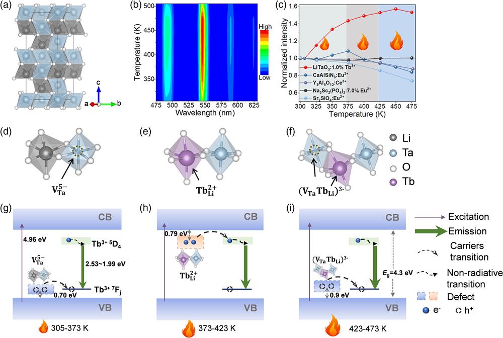
Here, we constructed three types of defect centers, including Ta vacancy (), Li substitution by Tb (), and complex defects by introducing into a highly structurally rigid and defect-tunable matrix with the space group [Fig. 1(a)]. At 373 and 473 K, the fluorescence intensity is about 1.4 and 1.5 times that at 305 K, manifesting a wide temperature range NTQ [Figs. 1(b) and 1(c)]. As shown in Fig. 1(c), the thermal stability of at temperatures up to 473 K exceeds that of the existing commercial and advanced phosphor materials.7 This NTQ is attributed to triple defects ,, and with trapping-depth-varied levels, as shown in Figs. 1(d)–1(f). They can effectively store charge carriers, thus acting as energy buffer layers in three consecutive temperature ranges of 305 to 373 K, 373 to 423 K and 423 to 473 K, respectively. Under thermal stimulation, the directional transport of the carriers from the defects to the activators can be continuously realized to compensate for the thermal loss from low to high temperatures, as depicted in Figs. 1(g)–1(i), thus achieving NTQ under a wide-range temperature. In other words, the luminescent source at high temperature originates from the itself and the supplement of the triple traps. This effect can compensate for the loss from the nonradiative processes and can thus suppress TQ. Triple defects have been confirmed by various advanced experimental techniques, including use of a high-resolution transmission electron microscope (HRTEM), positron annihilation lifetime spectroscopy (PALS), thermoluminescence (TL) spectroscopy, and first-principles theoretical calculations. Furthermore, with triple defects-induced NTQ demonstrates broad application prospects in temperature-dependent anti-counterfeiting and optical information storage.
Sign up for Advanced Photonics TOC. Get the latest issue of Advanced Photonics delivered right to you!Sign up now
![]()
Figure 1.NTQ performance and mechanism of
2 Materials and Methods
2.1 Synthesis of Phosphors
A series of (, 0.5%, 1%, 2%) phosphors were synthesized by high-temperature solid-state reaction. The starting materials (4N), (4N), and activator (4N) were used without further purification. The raw materials of phosphors activated by other elements (e.g., Eu) were also prepared using the corresponding oxides, such as (4N). First, the stoichiometric amounts of raw materials were ground in a mortar with an appropriate amount of anhydrous ethanol for 30 min until the complete evaporation of ethanol. Then, the mixture was pre-sintered for 2 h at 600°C in a muffle furnace, cooled to RT, and fully ground. It was finally sintered at 1100°C for 5 h in air to obtain the phosphors.
2.2 Material Characterization
X-ray diffraction (XRD) patterns of the as-prepared phosphors were recorded on a Bruker D8 ADVANCE X-ray diffractometer with Cu K radiation (). The composition and morphology of the powders were investigated on a JSM-6700F field emission scanning electron microscope as well as a JEM-2100F transmission electron microscope (Japan JEOL Corporation). X-ray absorption fine structure (XAFS) of Ta and Tb edge was obtained at Taiwan Light Source (BL17C1). XAFS data were processed using the Demeter XAS data processing package.24 For the Ta edge, the data were fit in R-space, from 1 to 2.4 Å. Two Ta-O paths of varied lengths were used in the fitting. The R-space extended X-ray absorption fine structure (EXAFS) signal was obtained by a variable -weighted Fourier transform () of the EXAFS signal over a -range of 3 to . Photoluminescence (PL) and photoluminescence excitation (PLE) spectra were recorded by a Hitachi F-4600 fluorescence spectrophotometer with a 150 W xenon arc lamp as the light source. The temperature-dependent PL spectra were measured with TAP-02 high-temperature fluorescence test accessories. TL spectra were conducted by an SL008 TL meter (Radiation Science and Technology Co. Ltd, Guangzhou, China). UV irradiation for 5 min was used to charge the phosphor particles. Until the afterglow dissipated, the sample was heated to a certain temperature at a rate of 1 K/s to record the signals. X-ray photoelectron spectroscopy (XPS) measurements were performed by electron spectroscopy for a chemical analysis system (Axis Ultra, Kratos analytical-A Shimadzu Group company) with an Al (Mono) source (150 W). In situ temperature-dependent Raman characterization was performed using a Renishaw inVia Laser confocal Raman Spectrometer. The laser wavelength was 523 nm. Raman spectra were collected in the temperature range from 305 to 498 K.
In a PALS experiment, a radioactive source was used as the positron source with a source intensity of about . Two identical samples were clamped on either side of a source to form a typical sandwich geometry. The conventional positron annihilation lifetime spectrometer uses a pair of scintillators to detect gamma rays released after positron annihilation. The positron annihilation lifetime spectrum was collected by the fast-slow coincidence measurement technology. The total lifetime spectrum number is 2 million to ensure the validity of the statistics. The time resolution of the spectrometer was 195 ps, and the electronic plug-in of the measurement system was the standard NIM plug-in of EG&G Company.
The performance of pressure sensing was studied by a laboratory-built integrated test system using a computer-controlled Shimadzu Universal stress testing instrument (AGS-X 10KN STD) with a photomultiplier tube (Hamamatsu photon, C13796) and a fluorescence spectrometer (SR-500I-B1-R, Andor).
2.3 Synthesis of Optical Information Storage Wafer
A certain amount of polydiethylsiloxane (PDMS) precursor and curing agent was put into a beaker, followed by adding phosphor particles with a phosphor/PDMS weight ratio of 0.4:1. After stirring evenly, the mixture was slowly poured into a 4 cm × 4 cm mold. A flexible wafer was obtained by heating and curing at 75°C for 1 h in an oven.
2.4 Preparation of Pressure Sensing Devices
The powder sample of was mixed with optical epoxy resin, followed by injection into a cylindrical mold container with a diameter of 20 mm and a height of 15 mm. After curing at 50°C for 6 h, the samples were taken from the mold. Before testing, the cured sample was exposed to UV radiation at 254 nm for 5 min.
2.5 DFT Theoretical Calculation
Theoretical calculation of the electronic structure was performed based on the density functional theory (DFT) implemented via the Vienna ab initio simulation package (VASP) code.25 Moreover, the exchange correlation potential is selected by the generalized gradient approximation (GGA) with the Perdew–Burke–Ernzerhof (PBE) formulation. The cutoff energy was 400 eV, and Brillouin zone integration was represented using the -point sampling scheme of a Monkhorst–Pack grid. The stopping criterion for ionic optimization number is , while the criterion for allowed error in total energy is . The formation energies () of with different defects were calculated by26
2.6 Calculation of Positron Annihilation Lifetime
Positron annihilation lifetime calculations were performed using an ABINIT software with two-component density-functional theory (TCDFT) calculations in the projector augmented-wave (PAW) framework. Calculations were performed using a supercell consisting of 120 atoms. In the defective structural models, a Ta vacancy () was built by removing a Ta atom from the supercell, and a Tb atom was further applied to substitute a Li atom to form a complex-defect .
3 Results
3.1 Structural Characterizations
The XRD patterns illustrate that all the as-prepared samples correspond well with standard hexagonal phase (PDF#29-0836) [Fig. 2(a) and Fig. S1 (see Supplementary Material)]. As shown in Fig. 2(b), the XRD Rietveld refinement of implies that the calculated data comply with the experimental measurements, where each Ta atom and Li atom are coordinated with six O atoms affording Ta-O and Li-O octahedron units (Table S1 in the Supplementary Material).27
![]()
Figure 2.Structural characterizations of
The HRTEM images of indicate that the lattice fringe with spacing of 0.372 nm corresponding to the (012) plane [Figs. 2(d)–2(e)] is well consistent with the refined structure of hexagonal phase . Also, the selected area electron diffraction (SAED) pattern taken along the axis of [] zone confirms the single-crystal nature of the phosphor particles [Fig. 2(f) panel (i)].30Figure 2(f) panels (ii)–(iv) show the filtered images of the regions within dashed white squares in Figs. 2(d) and 2(e). The atomic arrangement of Ta atoms observed from the images, as well as the recorded intensity profile verifies the phase of [– in Fig. 2(f)], consistent with the XRD refinement result. The filtered images display that the lattice fringes are discontinuous, and some lattice positions are blurred or even missing, indicating the existence of defects [Fig. 2(f) panels (iii) and (iv) and Figs. S2, S3 in the Supplementary Material].31 In contrast to the intensity profiles of perfect lattice , and with significant absence of Ta atoms (), Tb can be observed to occupy the position of Li atoms between the Ta atomic gap, forming the aliovalent substitution defects , as shown in . Furthermore, since the ionic radius of (, ) is larger than that of (, ), the doped (, ) with a large radius is inclined to occupy the lattice site. Also, the intensity distribution recorded along verifies the existence of the complex defects composed of adjacent and . These defects , , and are expected as capture sites with different depths for storing carriers, compensating for the TQ effect, and thus increasing the emission intensity of under high temperature.7,32
The formation of triple defects in was also investigated from the thermodynamic point of view by first-principles calculations. The formation energies () of possible defects, including , Li vacancy (), inequivalence defects and , as well as complex defects and , are calculated as shown in Fig. S4 in the Supplementary Material. The results show that , , and complex defect have lower formation energy than , , and , also verifying the existence of triple defects , , and as observed by HRTEM. Furthermore, the calculated energy band structures show that these defects have no significant effect on the bandgap (Fig. S5 in the Supplementary Material), but impact the electronic structure greatly. Density of states (DOS) of with these defects provides us with the specific effects of defects on the electronic structure [Figs. 2(h)–2(j)]. By comparing the total DOS profiles, with displays a higher occupied state at the bottom of the valence band (VB), leading to a better carrier storage capacity. It is evident that can form a new intermediate level near the conduction band (CB). As an energy buffer layer, it is mainly composed of orbitals, which can realize the ET from the defect level to the luminous level. Also, the presence of the complex defect has the same effect. A new intermediate level mainly consisting of orbitals appears near the VB. This indicates that the complex defect can effectively improve the -electron domination near the Fermi level, associated with the promoted carrier transfer.33 All these characterizations confirm the existence of triple defects with varied electronic structures in , which could act as the energy buffer layers to promote NTQ.
3.2 NTQ Behaviors and Defect Identification of LiTaO3:Tb3+ Phosphor
To have a closer insight into the effect of defects on NTQ, TL, as one of the most effective techniques for characterizing the type and depth of defects,34,35 was measured for the phosphor. The result demonstrates three successive temperature ranges of 300 to 373 K (), 373 to 423 K (), and 423 to 498 K (), indicating three significant trap levels induced by triple defects associated with , , and , respectively [Fig. 3(a) and Figs. S6, S7 in the Supplementary Material]. This result is consistent with the aforementioned computational defect formation energy for these triple defects. The trap depths of defects were calculated using the following empirical equation36:
![]()
Figure 3.Identification of defects in
To better elucidate how defects improve the NTQ performance of , the PALS combined with TCDFT calculation was performed to study the defect positron states, enabling the process of trapping and detrapping to be unambiguously established.37
The corresponding positron state, including positron lifetime and density, was calculated using TCDFT with ABINIT, as shown in Table S3 in the Supplementary Material and Figs. 3(e) and 3(f). The calculated lifetime of LiTaO3 with is 173.8 ps, which is close to the component (173.6 ps) of the experimental results. Meanwhile, the lifetime is 299 ps. Thus, it is evident that the main positron lifetime components and can be attributed to and complex defect , respectively. In addition, the value is also consistent with the reported positron lifetime range (170 to 200 ps) of B-site vacancy in perovskite oxides ABO3.42
To demonstrate the important role of triple defects in LiTaO3:1%Tb3+ in promoting NTQ, a series of samples with regulatory defects were designed and prepared for comparison, including LiTaO3:1% with reductive atmosphere treatment (), Li or Ta excessive or , and , co-doped phosphor. The TL curve of R- shows that the density of defects in remains unchanged, while those in and evidently decrease [Fig. 3(g)]. As expected, it shows weak NTQ in the low temperature range of 300 to 373 K, and TQ of PL emission can be detected as the temperature increases from 373 to 473 K [Fig. 3(h) and Fig. S11 in the Supplementary Material]. This is because the reducing atmosphere treatment increases the concentration of positively charged oxygen vacancy competing with the defect, thus eliminating the effects of and complex defect . For the samples with excessive Li or Ta alone [Fig. 3(h)], the defect content in the samples decreased, thus leading to significant TQ.
By comparing Eu3+ single-doped and Eu3+, Tb3+ co-doped LiTaO3 phosphors (Fig. S12 in the Supplementary Material), the TL results imply that co-doping Tb significantly enhances the thermal stability of phosphors ascribed to rich defects in the co-doped materials. This further certifies that the defects play an important role in suppressing TQ. In agreement with previous reports,45 upon increasing the temperature to 498 K, the PL dynamics in is accelerated by [effective lifetime from to , Fig. 3(i)], suggesting that carrier trapping is strongly enhanced at high temperatures. The improved carrier separation and transfer efficiency were also verified by photoelectrochemical experiments. Figure S13 in the Supplementary Material illustrates that has a larger current density and a smaller charge transfer resistance than . It shows the photogenerated electron-hole separation under UV radiation is better for .
3.3 Chemical Environments and Structures
Except for the defects effect, the chemical environments and intrinsic structures of and were also evaluated. In the XPS spectra of Ta [Fig. 4(a) and Fig. S14 in the Supplementary Material], shows the Ta and peaks at 26.2 and 28.3 eV, respectively, confirming the dominant oxidation state of , whereas for , these two peaks are shifted toward lower binding energy, which implies that the as-formed leads to a lower valence state.46 In the Li 1s spectra (Fig. S15 in the Supplementary Material), exhibits the peaks locating at 55.16 eV. For , the peak position shifts toward lower binding energy of 54.92 eV. This results from partial occupation of the Li sites by low concentration of . Raman spectroscopy is an important tool for studying phonon patterns and assessing local structures in the NTQ materials.3,47 As shown in Fig. 4(b), and represent the modes of Ta-O framework deformation.48 The ratio of increases from 1.1 to 1.5 when doping Tb3+, indicating that the defects induce the change of the Ta-O deformation.49
![]()
Figure 4.Chemical environments and structures of
In situ temperature-dependent Raman spectra are shown in Fig. 4(c). With the increase of temperature from 305 to 498 K, all Raman peaks become weaker in intensity and wider in shape, which is associated with the improvement of disordered or relaxation characteristics. There is a significant blueshift of the , , and vibrational modes, providing a favorable pathway for thermal activation enhancement. The O-Ta-O bending mode at () is strongly coupled with Li-O stretching () and Ta-O stretching (). The O-Ta-O bending () is almost constant with increasing temperature, suggesting that it could act as a structural buffer layer for thermally induced fluctuations to reduce thermal effects associated with the structural relaxation of the Tb3+ luminescent center. As the temperature increases, the phonon energy increases, and the ET from the defects to the luminescence energy level makes the lattice stable enough to suppress TQ. In addition, the reduction of the maximum phonon energy () may favor the luminescence of Tb3+ at high temperatures because the nonradiative relaxation could be effectively inhibited.47
The EXAFS data as well as the fitting results are shown in Fig. 4(d) and Fig. S16 and Table S4 in the Supplementary Material. The main peak at is attributed to the scattering interaction between Ta and O atoms (Ta-O). And the average bond length of Ta-O increases from 1.967 to 1.973 Å with the increase of Tb doping concentration, suggesting that the lattice expands due to the substitution of (, ) by large radius Tb ions (, ). Additionally, the increase of the coordination number of the Ta-O path further certifies the formation of defects in the material.50 Furthermore, the local electronic structure of Tb was detected by X-ray absorption near-edge spectroscopy (XANES). Different from the mixed valence state of reference sample Tb4O7, the Tb3+ activator in is stabilized with the trivalent state [Fig. 4(e) and Fig. S17 in the Supplementary Material], which is similar to the -doped nanoscintillators.16
3.4 DFT Calculations
To deeply understand how the defect structures affect the NTQ performance of , DFT calculations were carried out by constructing models with these three defects. The structural models are shown in Figs. 5(a1)–5(a3). Differential charge density calculations [Figs. 5(b1)–5(b3) and 5(c1)– 5(c3)] reveal the depletion of electrons at the negative charge defect and the accumulation at the positive charge defect . Moreover, there is a significant transfer of electrons from to at the complex defect . These results manifest that the accumulation and depletion of electrons at the defect sites are significantly increased. And the high electron/positron density in the defects facilitates the ET from the defects to the orbital in the luminescence center at high temperatures.51
![]()
Figure 5.DFT calculations of
The proposed NTQ mechanism of Tb3+-doped LiTaO3 with triple defects is shown in Fig. S18 in the Supplementary Material. There are three types of defects that can capture carriers (electrons and holes) activated by UV light. The carriers in the defect could be decaptured to compensate for the heat loss upon thermal stimulation, thus achieving negative thermal quenching (NTQ) at high temperatures. Specifically, and act as hole traps (h-traps), while acts as an electron trap. Under UV excitation, electrons and holes in the material could be separated, and holes in the VB are captured by the hole trap and , and electrons in the CB are captured by the electron trap , as shown in process (1). In the low-temperature region (300 to 373 K), holes in the shallowest trap are first decaptured to the luminescence centers (Tb3+) [process (2)], and then holes and electrons recombine to generate luminescence [process (3)]. In the mid-temperature region (373 to 425 K), the electrons stored in the trap of escape to the excited state level of Tb3+ and release energy in the form of luminescence. In the high-temperature region (425 to 475 K), the holes stored in the composite defect are released to compensate for the heat loss and thus lead to the NTQ behavior.
3.5 Applications in Temperature-dependent Information Encryption
Since the experimental and computational results indicate that multiple defect levels can trap and detrap optical energy, the phosphor could be very suitable for applications in temperature-dependent information encryption and anti-counterfeiting. To demonstrate information storage capability mediated by triple defects with different trapping depths, we design a temperature-dependent decrypting algorithm, as shown in Fig. 6(a).
![]()
Figure 6.Applications in temperature-dependent decryption, multiple-information storage, and pressure sensing. (a) Schematic diagram of temperature-dependent decrypting process. The information is encrypted by UV irradiation at 298 K. The rise of the temperature to 353 K results in a readout of
First, the optical information storage film consisting of phosphor and PDMS was encrypted by UV light irradiation at 298 K. Then it was heated to three temperature zones in order to decrypt the information [Fig. 6(a)]. Figure 6(b) shows the TL curves of temperature-dependent decrypting with triple defects. The information decoding photos for the corresponding processes in Figs. 6(a) and 6(b) are shown in Fig. 6(c). The information was decrypted in the form of bright green light emission. At 353 K, the luminescence intensity changed from bright to dimming in 60 s, indicating that trap was emptied first. Upon being continuously heated to 398 and 453 K, the luminous intensity also shifted from bright to dim, manifesting that traps and were also emptied in order. Moreover, after each heating and de-trapping process, the use of UV charging can restore the carriers in the traps. By tailoring the heating duration from 0 to 80 s after UV charging, it can be clearly seen that under thermal stimulation, the stored charge carriers were released in the form of luminescence. The higher the temperature, the faster the charge carriers are released, and the shorter the duration of the thermally excited luminescence (Fig. S19 in the Supplementary Material).
Since the designed pattern information can be encrypted and decrypted intuitively, we also designed a pattern-based encoding method for multiple information encryption [Figs. 6(d) and 6(e) and Figs. S20 and S21 in the Supplementary Material]. First, the whale pattern information was encrypted into the phosphor film using UV light irradiation at 298 K [Fig. 6(d)], followed by a partial readout of the information at 423 K on a hot stage. After cooling to RT, the encryption of the horse pattern was performed and the partial information was emptied again at 373 K. After cooling, the butterfly pattern was encrypted by UV irradiation. The removed information for three patterns is not visible at RT. As the temperature increases from 353, 398, and 453 K, the encrypted patterns butterfly, horse, and whale could be decrypted sequentially [Fig. 6(e)]. The emission spectra at the corresponding temperatures were also recorded. Therefore, high-security and multidimensional information storage using LiTaO3:Tb3+ phosphor with trapping-depth-varied triple defects can be achieved by precisely controlling the heating temperature and encrypting different pattern information.
It is worth noting that the charge carriers stored in the defects also could be stimulated by pressure, which shows potential application of LiTaO3:Tb3+ phosphor in pressure sensing. Figure 6(f) demonstrates that the visual and continuous decryption of information can be achieved by applying pressure to an organic composite block made of LiTaO3:Tb3+ phosphor after 5 min of UV charging. The encrypted information was about 35% of its original intensity after 10 cycles of pressure loading, and the continuous luminescence could be observed by applying pressure onto the composite block [Fig. 6(g)]. Furthermore, the decryption of the information could also be achieved by a 980-nm laser (Fig. S22 in the Supplementary Material). The photo-stimulated luminescence spectrum is completely consistent with the emission spectra recorded under heating and stress, indicating that all this luminescence originates from Tb3+. Therefore, the carriers in the defects could achieve a triple thermal, mechanical, and optical response, which provides a new strategy for developing temperature-dependent information encryption, multidimensional information storage, as well as press sensing.
4 Conclusion
In summary, triple defects , , and with varied trapping depths, which were identified by HRTEM, PALS, TL, and first-principles calculations, have been constructed into a LiTaO3 lattice by doping . The optimized phosphor exhibits a significant NTQ effect over a wide temperature range of up to 473 K, implying the potential applications in temperature-dependent anti-counterfeiting. The superior NTQ of phosphor is mainly ascribed to triple defects ,, and , which act as energy buffer layers to mitigate emission loss in three successive temperature zones, thus suppressing TQ in a wide temperature range. Furthermore, the multidimensional information encryption and decryption could be realized based on the temperature-dependent response behaviors of triple defects. This work opens a new avenue for the exploration of multiple defects-induced NTQ phosphors for high temperature and information-decrypting applications.
Acknowledgment
Acknowledgment. The authors acknowledge financial support from the National Key Research and Development Program of China (Grant No. 2018YFB0704103), the Natural Science Foundation of Shanghai (Grant Nos. 22ZR1472100 and 20ZR1465900), the National Natural Science Foundation of China (Grant Nos. 92163117 and 62175210), the State Key Laboratory of ASIC & System (Grant No. 2020KF002), and the Innovation Project of Shanghai Institute of Ceramics (Grant No. E21ZC1770G). L. L. thanks the Taiwan Light Source for technical support. J. W. thanks the Program of Shanghai Academic Research Leader (Grant No. 20XD1424300) for financial support. The authors thank Professor Zhijun Zhang for providing valuable assistance in stress luminescence testing.
Mingxue Deng is a research intern at Shanghai Institute of Ceramics, Chinese Academy of Sciences (SICCAS). She received her BS degree from Northeastern University in 2018, and MS degree from SICCAS in 2021. Her main research interest concentrates on designing rare earth optical functional materials via high-throughput methods for optical storage, high power lighting and sterilization applications.
Xingzhong Cao is currently a full professor at Institute of High Energy Physics (IHEP), Chinese Academy Sciences. He received his PhD degree from Lanzhou University, China, in 2004. Before joining IHEP in 2010, he worked at KEK and Kyoto University of Japan for four years. His research interests include the technical development of positron annihilation spectroscopy and slow positron beam, and their application for the characterization of lattice defects in solid materials and the study of internal relationships between the macroscopic properties of materials and atomic scale microscopic defect structures.
Zhenzhen Zhou is an associate professor at Shanghai Institute of Ceramics, Chinese Academy of Sciences (SICCAS). She graduated from Hebei Normal University with BS and MS degrees in 2008 and 2011, respectively, and received her PhD degree from SICCAS in 2019. She has worked at SICCAS since 2011, mainly engaged in the research of high-throughput experimental methodology, fluorescent materials, scintillation materials, and other optical functional materials and devices.
Jiacheng Wang is currently a full professor of functional materials at Shanghai Institute of Ceramics, Chinese Academy of Sciences (SICCAS). He obtained his PhD from SICCAS in 2007. Before getting back to SICCAS in 2013, he spent six years on functional materials research at the University of Tokyo (collaborator: Prof. Makoto Onaka), Dresden University of Technology (collaborator: Prof. Stefan Kaskel), and Cardiff University (collaborator: Prof. Graham Hutchings). He was an Alexander von Humboldt Fellow, JSPS Postdoctoral Fellow for Foreign Researcher, and Marie Curie Intra-European Fellow. His present research focuses on rational design and preparation of advanced functional materials for energy transformation and photoluminescence.
Qian Liu is a full professor at Shanghai Institute of Ceramics, Chinese Academy of Sciences. She received BS and MS degrees from Tianjin University in 1982 and 1987, respectively, and a PhD degree from Shanghai Institute of Ceramics, Chinese Academy of Sciences, in 1994. Her research interests are the application of high-throughput technology for the rapid discovery and preferential selection of new materials and material systems, including luminescent materials, dielectric materials, steel materials, etc.
Biographies of the other authors are not available.

Set citation alerts for the article
Please enter your email address
© Copyright 2018-2021 | Chinese Laser Press. All Rights Reserved 沪ICP备15018463号-20