• Advanced Photonics
  • Vol. 4, Issue 4, 046004 (2022)
Zhixia Xu1、2、†, Jie Chang2, Jinye Tong2, Daniel F. Sievenpiper3、*, and Tie Jun Cui1、*
Author Affiliations
  • 1Southeast University, State Key Laboratory of Millimeter Waves, Nanjing, China
  • 2Dalian Maritime University, School of Information Science and Technology, Dalian, China
  • 3University of California San Diego, Department of Electrical and Computer Engineering, San Diego, California, United States
  • show less
    DOI: 10.1117/1.AP.4.4.046004 Cite this Article Set citation alerts
    Zhixia Xu, Jie Chang, Jinye Tong, Daniel F. Sievenpiper, Tie Jun Cui. Near-field chiral excitation of universal spin-momentum locking transport of edge waves in microwave metamaterials[J]. Advanced Photonics, 2022, 4(4): 046004 Copy Citation Text show less

    Abstract

    Controlling energy flow in waveguides has attractive potential in integrated devices from radio frequencies to optical bands. Due to the spin-orbit coupling, the mirror symmetry will be broken, and the handedness of the near-field source will determine the direction of energy transport. Compared with well-established theories about spin-momentum locking, experimental visualization of unidirectional coupling is usually challenging due to the lack of generic chiral sources and the strict environmental requirement. In this work, we design a broadband near-field chiral source in the microwave band and discuss experimental details to visualize spin-momentum locking in three different metamaterial waveguides, including spoof surface plasmon polaritons, line waves, and valley topological insulators. The similarity of these edge waves relies on the abrupt sign change of intrinsic characteristics of two media across the interface. In addition to the development of experimental technology, the advantages and research status of interface waveguides are summarized, and perspectives on future research are presented to explore an avenue for designing controllable spin-sorting devices in the microwave band.

    1 Introduction

    The quantum spin-Hall state is an electronic surface state with immunity against defects.1 The momentum is locked to the intrinsic spin of electrons, and backward transports are suppressed unless the spin flips.2,3 Analogous phenomena have been widely reported in various uniform and metamaterial waveguides, where theories of universal spin-momentum locking4 and spin-orbit interactions5,6 have been well studied. Uniform waveguides include closed metal waveguides, fibers, and plasmonic metals, where the unidirectional transmission can be realized based on nano-gratings,7 circularly polarized (CP) dipoles or Huygens dipoles8,9 supported by resonant particles.1014 Metamaterial waveguides consist of various artificial unit cells, where chiral sources carrying spin angular momentum (SAM) and orbital angular momentum (OAM) can interact with unit cells in versatile ways to realize unidirectional coupling.15 Recent research interest is mainly in metamaterial interfaces supporting edge waves. As shown in Fig. 1(a), two metamaterials are stitched together to construct an infinitely thin interface to support edge waves, such as spoof surface plasmon polaritons (SPPs), line waves (LWs), and photonic topological insulators (PTIs). All these kinds of edge waves are related to flipping change of intrinsic characteristics of media across the interface, as shown in Figs. 1(b)1(d).

    Spin-momentum locking exists at the interface of two metamaterials. (a) The chirality of the source decides the transmission direction. Unidirectional transmission at the interface between: (b) spoof SPPs: air and corrugated structures (εair>0, εeff<0); (c) LWs: dual-impedance surfaces (ZTM>0, ZTE<0); and (d) PTIs: Berry phase flips.

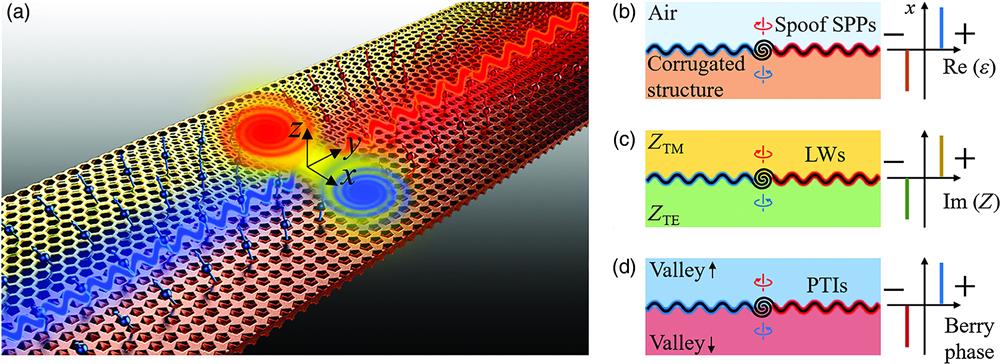
    Figure 1.Spin-momentum locking exists at the interface of two metamaterials. (a) The chirality of the source decides the transmission direction. Unidirectional transmission at the interface between: (b) spoof SPPs: air and corrugated structures (εair>0, εeff<0); (c) LWs: dual-impedance surfaces (ZTM>0, ZTE<0); and (d) PTIs: Berry phase flips.

    It is beneficial to further design generic chiral sources and visualize unidirectional coupling in different metamaterial waveguides. Spoof SPPs exist on the interface between the dielectric medium with positive permittivity (εair>0) and periodic metallic structures with negative effective permittivity (εeff<0),1619 as shown in Fig. 1(b). Spoof SPPs contain fruitful phenomena related to spin-orbit momentum.20,21 It is convenient to use modulated gratings to couple CP spatial waves to unidirectional spoof SPPs on an open metasurface.22 However, it is challenging to apply similar technology to one-dimensional infinitely thin spoof SPPs transmission lines23,24 due to the small cross section. Therefore, one purpose of this work is to develop a near-field chiral source to visualize spin-momentum locking in spoof SPPs transmission lines. LWs exist in the interface of a pair of metasurfaces with duality symmetry, such as reactance duality (ZTM>0 and ZTE<0)2527 or resistance duality (gain and loss),28 as shown in Fig. 1(c). LWs have been experimentally observed by linearly polarized feedings;29,30 however, unidirectional coupling stays in the simulation stage,28,29 where related experiments are still lacking. Therefore, the second part of this work is to visualize the spin-momentum locking of LWs. PTIs show flipping Berry phase in topological space, as shown in Fig. 1(d). The chirality of eigenmodes of unit cells determines the robust transmission direction along the edge.31,32 Spin-momentum locking can be realized with a linearly polarized source in Chern PTIs because the time symmetry is broken.3335 However, in valley topological waveguides, chiral eigenmodes require spin-orbit coupling.36 The coupling theory was first studied in a pseudo-spin structure37 and proved by experiments.38 Connections between OAM and valley transmission were also reported.39,40 It is important to further measure unidirectional valley PTIs, which is the third part of this work.

    This work presents near-field experiments to visualize unidirectional edge waves in various metamaterial waveguides. By flipping the chirality of the source, we can control the direction of energy coupling. The presented experimental methodology is universal and tutorial to realize spin-sorting metamaterial devices in the microwave band. We further compare characteristics of different waveguides, summarize research status, and present perspectives regarding the following challenges and future spin-sorting metamaterial devices implanted with modern coding techniques.

    2 Results

    2.1 Angular Momentum

    Chiral sources carrying SAM and OAM are the key to couple metamaterial waveguides with spin-momentum locking. Figures 2(a) and 2(b) show two feeding configurations used in this work.

    Two chiral sources carrying (a) SAM and (b) OAM. (c) Spin-momentum locking phenomenon. (d) SAM-OAM conversion. (e) Five-ports-feeding network and measured performance: (f) balanced amplitude and (g) π/2-phase step.

    Figure 2.Two chiral sources carrying (a) SAM and (b) OAM. (c) Spin-momentum locking phenomenon. (d) SAM-OAM conversion. (e) Five-ports-feeding network and measured performance: (f) balanced amplitude and (g) π/2-phase step.

    SAM (helicity σ=±1) is realized by the spinning electric vector consisting of orthogonal electric components with π/2-phase difference. We take a short review of the spin-momentum locking theory.4 The complex wavevector of evanescent waves is in a general form as k=k+ik. k is the real part related to the phase constant, and k is the imaginary part related to the decay. k and k are orthogonal, and we can divide evanescent waves into two polarizations denoted by s^ and p^. s^ is perpendicular to the plane formed by k and k, while p^ is in the plane, s^=ik×k*|k×k*|,p^=ik×(k×k*)|k||k×k*|,and, we further substitute the complex form of wavevector into Eq. (2) and obtain p^=i[k|k|(kk)+ik|k|(kk)],where the combination of orthogonal vectors indicates a π/2-phase difference in p^, verifying an elliptically polarized field whose spin direction can be represented by the purely real s^. As the slow-wave effect is enhanced, both real and imaginary parts of the wavevector become larger (|k||k|k0), and the field becomes nearly perfectly CP. Therefore, we can lock the direction of coupling by placing a CP source around the interface, as shown in Fig. 2(c). As examples, various CP-sensitive metamaterials were proposed to realize unidirectional performance.41,42

    OAM is dependent on the chiral phase distribution of the field. The polarization of the probes is identical, but the chiral phase carries OAM with the vortex charge (l=0,±1,±2), which represents the total phase change (2π×l) along a closed circle. SAM and OAM can transfer between each other by focusing or scattering.6,43 As shown in Fig. 2(d), assuming an incoming CP electric field (E) in the global circular basis of (x+iσy)-polarizations and the z component, we can obtain the scattering field (Es) from a particle as43Es=[1+abei2ϕ2abeiϕbei2ϕ1+a2abeiϕ2abeiϕ2abeiϕ2b2]E,where a=cos2θ and b=sin2θ. The off-diagonal elements are responsible for SAM-OAM conversion, which is the theoretical background for unidirectional coupling based on lens and nanoparticles.11,44,45

    To feed the chiral probe array, we designed a broadband power divider with the π/2-phase-shifting function. Figure 2(e) shows the five-port feeding network designed for measurements. The fabricated circuit consists of three power-dividers and three pairs of phase shifters,46 whose detailed structure is presented in the Supplementary Material. Figures 2(f) and 2(g) show the measured amplitude and phase relationships at different ports. Results indicate that signals at the four out-ports keep almost the same amplitude with the desired phase shift from 5 to 12 GHz.

    2.2 Spoof SPPs

    The proposed platform to observe spoof SPPs is shown in Fig. 3(a), where ideal absorptive terminals are based on two kinds of slots loading with gradient resistors,47 as shown in Fig. 3(b). The corrugated metallic structure supports spoof SPPs on the interface, and the electric field vectors have spin momentum, deciding the energy transport direction shown in Fig. 3(c). The depth of the slot decides the cut-off frequency of spoof SPPs, as shown in Fig. 3(d). When the frequency is above 5 GHz and below 15 GHz, the shallow slots can support spoof SPPs, while deep slots avoid detouring waves. Therefore, spoof SPPs are bounded along the route along the y axis. Animated comparisons of spoof SPPs on different structures are shown to demonstrate the importance of the terminal designs.

    (a) Spoof SPPs under study. (b) Enlarged absorptive terminal design. (c) Electric field vector of spoof SPPs with spin-momentum locking. (d) Dispersion curves of two spoof SPPs (SSPPs).

    Figure 3.(a) Spoof SPPs under study. (b) Enlarged absorptive terminal design. (c) Electric field vector of spoof SPPs with spin-momentum locking. (d) Dispersion curves of two spoof SPPs (SSPPs).

    The experimental setup is shown in Fig. 4(a). The CP source consists of a pair of orthogonal electric probes of negligible electric size and is placed at the center of the structure. With the CP source, we use two linearly polarized electric probes to record the transmission energy at two terminals of the structure. The right hand circularly polarized (RHCP) source can direct energy toward the right, and the energy level received at the left terminal is much lower, as shown in Fig. 4(b). We further set up RHCP and left hand circularly polarized (LHCP) sources to record the energy distribution along the edge, as shown in Fig. 4(c), verifying that sources with opposite chirality can direct energy toward opposite directions. The two-dimensional (2D) electric field distribution of the planar structure is shown in Fig. 4(d), where the forward transport is much stronger than the backward transport. Figure 4(e) demonstrates a conformal situation where spoof SPPs can travel on a curved surface and unidirectional coupling can still be observed in Fig. 4(f), indicating the robustness of spin-momentum locking on the flexible surface. Experiments match well with simulations, as shown in Videos 1 and 2.

    Visualization of unidirectional spoof SPPs. (a) The near-field scanning setup. (b) Transmission at two opposite terminals excited by an RHCP source. (c) Measured distribution of the out-of-plane electric field (Ez) at 10 GHz along the transmission route. (d) Field distributions on the 2D surface. (e) The planar structure is wrapped on the surface of a cylinder. (f) Unidirectional coupling on the surface of the cylinder [unidirectional planar spoof SPPs (Video 1, MP4, 2.26 MB [URL: https://doi.org/10.1117/1.AP.4.4.046004.1]) and unidirectional conformal spoof SPPs (Video 2, MP4, 1.59 MB [URL: https://doi.org/10.1117/1.AP.4.4.046004.2)].

    Figure 4.Visualization of unidirectional spoof SPPs. (a) The near-field scanning setup. (b) Transmission at two opposite terminals excited by an RHCP source. (c) Measured distribution of the out-of-plane electric field (Ez) at 10 GHz along the transmission route. (d) Field distributions on the 2D surface. (e) The planar structure is wrapped on the surface of a cylinder. (f) Unidirectional coupling on the surface of the cylinder [unidirectional planar spoof SPPs (Video 1, MP4, 2.26 MB [URL: https://doi.org/10.1117/1.AP.4.4.046004.1]) and unidirectional conformal spoof SPPs (Video 2, MP4, 1.59 MB [URL: https://doi.org/10.1117/1.AP.4.4.046004.2)].

    2.3 LWs

    Two metasurfaces with opposite reactance are designed, as shown in Fig. 5(a), where the enlarged illustration shows the configuration of a CP source with a pair of orthogonal electric dipoles with a π/2-phase difference. The periodic serpentine acts as an inductive surface and can be named ZTM surfaces because the fundamental surface mode is transverse magnetic (TM) polarization. The interdigitated patch array acts as a capacitive surface and can be named ZTE surfaces because the fundamental surface mode is transverse electric (TE) polarization. The cross section of the electric field distribution is shown in Fig. 5(b). The electric field vector is mainly perpendicular to the ZTM surface but parallel to the ZTE surface. At the interface between two surfaces, energy is concentrated, and electric field vectors twist. Simulated dispersion curves of two surface modes and LWs are plotted in Fig. 5(c), and the equivalent surface reactance can be extracted from the phase constant.29 The authors proposed and analyzed the structures recently,29 but related experiments to visualize the spin-momentum locking are challenging and have been solved in this work.26,27,29,48

    (a) Structure of the LWs waveguide under study. (b) Electric field distribution at the x-z cross section. (c) Dispersion curves of surface modes and LWs, and equivalent surface reactance can be calculated. Black solid line: dispersion curves of surface waves and LWs. Gray dashed line: light cone. Colored dashed line: extracted surface impedance.

    Figure 5.(a) Structure of the LWs waveguide under study. (b) Electric field distribution at the x-z cross section. (c) Dispersion curves of surface modes and LWs, and equivalent surface reactance can be calculated. Black solid line: dispersion curves of surface waves and LWs. Gray dashed line: light cone. Colored dashed line: extracted surface impedance.

    We set up the experimental environment as shown in Fig. 6(a). CST Studio Suite is utilized to conduct simulations, and results are shown in Fig. 6(b). The CP source is placed beneath the metasurface. A linearly polarized probe is used to record the electric field distribution on the surface. The measured electric field distribution is shown in Fig. 6(c). Excited by the LHCP source, energy is directed toward the left side. We compare the animation of simulated and measured field distributions in Video 3, and the consistency can verify the existence of unidirectional transport. The visualization of LWs is not as clear as that of spoof SPPs because two metasurfaces on both sides can support the surface waves whose operating frequencies overlap with LWs, as shown in Fig. 5(c). It is challenging to suppress the unwanted surface waves when we excite the LWs with a CP source that has the omnidirectional radiation pattern. More work remains to be done to improve the structure of feeding probes.

    Visualization of unidirectional LWs. (a) The near-field scanning setup. (b) Simulated electric field (Ez) distribution on the surface of the planar structure where we set up uniform equivalent impedance surfaces as a simplified simulation model. (c) Measured electric field (Ez) distribution [unidirectional LWs (Video 3, MP4, 2.99 MB [URL: https://doi.org/10.1117/1.AP.4.4.046004.3])].

    Figure 6.Visualization of unidirectional LWs. (a) The near-field scanning setup. (b) Simulated electric field (Ez) distribution on the surface of the planar structure where we set up uniform equivalent impedance surfaces as a simplified simulation model. (c) Measured electric field (Ez) distribution [unidirectional LWs (Video 3, MP4, 2.99 MB [URL: https://doi.org/10.1117/1.AP.4.4.046004.3])].

    2.4 PTIs

    The valley waveguide under study is based on 10-mm height alumina rods with two PEC plates on top and bottom layers to restrict waves in the structure as TM modes with an out-of-plane electric field (Ez), as shown in Fig. 7(a). A cardboard made by a laser engraving procedure is placed in the middle of two PEC plates to fix dielectric rods. Figure 7(b) shows the analysis of the unit cell. We can observe the opening of the Dirac cone at highly symmetric points when the structure transforms from C6- to C3-symmetric, and the corresponding intrinsic OAM (l=±1) of the eigenmode is reflected in the phase distribution.39 Therefore, we can place a chiral source with OAM (l=±1) at the center of a unit cell to couple the unidirectional valley transport. The Berry curvature is calculated based on the four-point formula procedure.49 The superlattice simulation is shown in Fig. 7(c); the dispersion curves and energy confinement at the interface verify the existence of topological edge waves within the bandgap.

    (a) The valley waveguide. (b) Unit cell analysis: topological bandgap, intrinsic OAM (l=±1), and flipping Berry curvature. (c) Superlattice analysis: dispersion and field distributions of valley PTIs at two different interfaces. Unidirectional OAM coupling with (d) different vortex charges l and (e) different phase step Δφ. The transmission is defined by the proportion of received energy at terminals (left/right) and the total energy of the source: T=Pleft/right/Psource. The maximum transmission (T=1) represents an ideal unidirectional coupling.

    Figure 7.(a) The valley waveguide. (b) Unit cell analysis: topological bandgap, intrinsic OAM (l=±1), and flipping Berry curvature. (c) Superlattice analysis: dispersion and field distributions of valley PTIs at two different interfaces. Unidirectional OAM coupling with (d) different vortex charges l and (e) different phase step Δφ. The transmission is defined by the proportion of received energy at terminals (left/right) and the total energy of the source: T=Pleft/right/Psource. The maximum transmission (T=1) represents an ideal unidirectional coupling.

    It is interesting to further discuss the performance of different OAM sources. We consider two parameters: different vortex charge |l| and different phase stepping Δφ. By modeling different sources (Supplementary Material), we analyze the corresponding unidirectional coupling spectra, as shown in Figs. 7(d) and 7(e). Two findings are summarized as follows.

    The experimental setup is shown in Fig. 8(a), where the source carrying OAM (l=1) is placed in the center of a unit cell beside the interface. It is a general concept that robust unidirectional PTIs can radiate at open terminals without obvious reflection.36 However, it is still unclear whether we can change the terminal shape without generating reflection. Inspired by horn antennas, we propose a horn-type terminal to guide valley PTIs toward the center of the open terminal as shown in Fig. 8(b). The traditional open terminal36 as a counterpart has a splitting distribution at the aperture. We record the field distributions at different terminals to verify the correctness of the simulation, as shown in Fig. 8(c). The concentrated and the splitting distributions match well with simulations, although the unidirectional coupling exists in both structures. Transmission is recorded by a linearly polarized probe, as shown in Fig. 8(d), where unidirectional valley PTIs exist within the bandgap. Animations of the valley PTIs at different terminals are compared in Videos 4 and 5.

    Visualization of unidirectional valley PTIs. (a) Near-field scanning setup. (b) Simulated electric field distributions of two waveguides with horn-type and straight-line-type terminals. (c) Measured electric field distribution at opposite terminals. (d) Measured unidirectional transmission [unidirectional valley PTIs with the horn-type terminal (Video 4, MP4, 1.32 MB [URL: https://doi.org/10.1117/1.AP.4.4.046004.4]) and unidirectional valley PTIs with the straight-line-type terminal (Video 5, MP4, 1.26 MB [URL: https://doi.org/10.1117/1.AP.4.4.046004.5])].

    Figure 8.Visualization of unidirectional valley PTIs. (a) Near-field scanning setup. (b) Simulated electric field distributions of two waveguides with horn-type and straight-line-type terminals. (c) Measured electric field distribution at opposite terminals. (d) Measured unidirectional transmission [unidirectional valley PTIs with the horn-type terminal (Video 4, MP4, 1.32 MB [URL: https://doi.org/10.1117/1.AP.4.4.046004.4]) and unidirectional valley PTIs with the straight-line-type terminal (Video 5, MP4, 1.26 MB [URL: https://doi.org/10.1117/1.AP.4.4.046004.5])].

    3 Perspectives

    Based on the generic chiral sources, we conducted microwave experiments to visualize unidirectional coupling in different metamaterial waveguides. We compare the key characteristics in Table 1 and present perspectives regarding applications and challenges in the future.

    Metamaterial waveguidesChiral sortingWorking bandwidthWave velocityTransmission robustnessPotential applicationsDevice-assisted
    Spoof SPPsSAM/OAMBroadbandSlowFlexibilityWearable, compact circuitsVigorous
    LWsSAM/OAMBroadbandSlowFlexibilityMultifunctional metasurfacesUnexplored
    PTIsSAM/OAMNarrowSlow/fastImmunityIsolators and cavitiesEarly stage

    Table 1. Characteristics of Three Waveguides in the Microwave Band

    Three waveguides all have chiral sorting abilities. Incident waves with SAM and OAM can excite the unidirectional transmission.7,50 As similar evanescent waves, LWs inherit most features of spoof SPPs, but the unidirectional LWs based on OAM remain unsolved. Unlike the spoof SPPs and LWs stemming from the complex wavevector of evanescent waves, the unidirectional PTIs rely on the eigenmodes carrying SAM and OAM.36,37,39 Spoof SPPs and LWs can exist over a broad band, indicating the potentials in broadband communication systems;51 however, PTIs only exist within a narrow photonic bandgap. The narrow bandwidth of PTIs limits the communication capability but has advantages in designing high-Q and robust cavities in laser applications.52,53 Another difference is the wave velocity. Spoof SPPs and LWs are slow waves, while the closed PTIs waveguides can support both slow and fast waves without leakage. From the perspective of assembly process, people can use flexible substrates, such as polyimide, to guide the spoof SPPs and LWs along curved surfaces,18,23,29 indicating the potential applications in wearable networks.54 PTIs usually exist in solid hole-slab or pillars, losing the flexibility. However, the unique immunity against defects is under topological protection, which can be the key for non-reciprocal devices33,34,55 and on-chip high robust links.56,57

    The scale of semiconductor devices is much smaller than the wavelength; therefore, it is crucial to explore device-assisted metamaterials beyond the conventional structural designs. Recently, plenty of exotic spoof SPPs components have been reported,58 such as parametric amplifiers,59 active Fano sensors,60 and nonlinear harmonic generators.61 Compared to vigorous active spoof SPPs, the device-assisted technology is still a virgin land in LWs and PTIs because they require loading devices in the form of 2D arrays. The concept of device-assisted LWs was first reported as a terahertz tunable simulation model based on graphene,62 lacking further experimental work. Meanwhile, the first device-assisted PTIs platform was reported recently,63 and more fruitful work remains to be explored.

    The future direction of spin-sorting metamaterials could be in the hybrid form of massive loading devices and novel structures. Related embedding fabrication and controlling technologies have shown significant achievements in recent digital coding metasurfaces64,65 and will be transferred to the field of spin-sorting metamaterials. Combining the device-assisted metamaterials and controllable feeding circuits, we can tailor metamaterial waveguides and the source carrying angular momentum simultaneously. Furthermore, we illustrate some research directions to be explored in Fig. 9. The digital coding spoof SPPs have been widely discussed in recent years, and many tunable devices have been reported.66,67 However, the degree of chiral freedom has not been fully implanted into the spoof SPPs systems. Dynamic control of the energy flow is possible based on the experimental technology reported in this work. Coding LWs is more complex than the spoof SPPs, but some exciting potentials are unique. The digital coding impedance characteristics can construct arbitrary transmission routes on the surface. Meanwhile, the scattering from metasurface decided by surface impedance68 can be fully controllable, indicating a powerful platform to control surface and space waves at the same time. Future research on the coding PTIs can be focused on dynamic tailoring of the topological invariant, which decides the edge modes on the interface. Combining the recent progress in the topological radiation,6971 we can further develop robust multiplexers and antenna arrays, which will be highly integrated with future wireless systems.

    Digital coding metamaterial waveguides with spin-momentum locking. (a) Spoof SPPs: manipulating the wavevector and bi-directional chiral sorting. (b) LWs: manipulating impedance to tailor the arbitrary transmission and control the scattering performance of metasurfaces at the same time. (c) PTIs: manipulating the topological invariant to realize dynamic chiral sorting multiplexers.

    Figure 9.Digital coding metamaterial waveguides with spin-momentum locking. (a) Spoof SPPs: manipulating the wavevector and bi-directional chiral sorting. (b) LWs: manipulating impedance to tailor the arbitrary transmission and control the scattering performance of metasurfaces at the same time. (c) PTIs: manipulating the topological invariant to realize dynamic chiral sorting multiplexers.

    4 Conclusion

    We developed the experimental technologies to visualize the unidirectional transports of edge waves in three different metamaterial waveguides in the microwave band. The key mechanism behind spoof SPPs, LWs, and PTIs is the abrupt sign change of different intrinsic properties of artificial media across the interface. We discussed the advantages and research status and presented an outlook for future metamaterial devices based on modern digital coding technology and controllable spin-momentum locking.

    Zhixia Xu received his BSc degree in electronic information science and technology from Dalian Maritime University, Dalian, China, in 2015, and a PhD in electromagnetic field and microwave technique from Southeast University, Nanjing, China, in 2019. From 2018 to 2019, he worked as a visiting scholar at the University of California San Diego, California, United States. He is currently an associate professor at Dalian Maritime University. He also holds a postdoctoral position at the State Key Laboratory of Millimeter Waves, Southeast University. His current research is focused on photonic topological insulators.

    Jie Chang received his BE degree in communication engineering from Dalian Maritime University, Dalian, China, in 2020, where he is currently pursuing an ME degree. His current research is focused on photonic topological insulators.

    Jinye Tong received her BE degree in communication engineering from Dalian Maritime University, Dalian, China, in 2020, where she is currently pursuing an ME degree. Currently, she is involved in the design of frequency selective surfaces.

    Daniel F. Sievenpiper received his BS and PhD degrees in electrical engineering from the University of California, Los Angeles, California, United States, in 1994 and 1999, respectively. He is a professor at the University of California, San Diego, California, United States, where his research is focused on artificial media. He was a recipient of the URSI Issac Koga Gold Medal, the Piergiorgio Uslenghi Letters Prize Paper Award, and the John D. Kraus Antenna Award.

    Tie Jun Cui is a chief professor at Southeast University, Nanjing, China; an academician of the Chinese Academy of Sciences; and a director of State Key Laboratory of Millimeter Waves. His research is focused on metamaterials. He proposed the concepts of digital coding and programmable metamaterials, and founded a new direction of metamaterials: information metamaterials, which can manipulate the electromagnetic fields and process the digital information simultaneously.

    References

    [1] C. L. Kane, E. J. Mele. Quantum spin Hall effect in graphene. Phys. Rev. Lett., 95, 226801(2005).

    [2] B. A. Bernevig, S.-C. Zhang. Quantum spin Hall effect. Phys. Rev. Lett., 96, 106802(2006).

    [3] A. Javadi et al. Spin–photon interface and spin-controlled photon switching in a nanobeam waveguide. Nat. Nanotechnol., 13, 398-403(2018).

    [4] T. Van Mechelen, Z. Jacob. Universal spin-momentum locking of evanescent waves. Optica, 3, 118-126(2016).

    [5] K. Y. Bliokh, D. Smirnova, F. Nori. Quantum spin Hall effect of light. Science, 348, 1448-1451(2015).

    [6] K. Y. Bliokh et al. Spin–orbit interactions of light. Nat. Photonics, 9, 796-808(2015).

    [7] J. Lin et al. Polarization-controlled tunable directional coupling of surface plasmon polaritons. Science, 340, 331-334(2013).

    [8] M. F. Picardi, A. V. Zayats, F. J. Rodríguez-Fortuño. Janus and Huygens dipoles: near-field directionality beyond spin-momentum locking. Phys. Rev. Lett., 120, 117402(2018).

    [9] D. Yi et al. Regulating the direction that power flows in microwave transmission line systems with Huygens sources. IEEE Trans. Antennas Propag., 69, 594-599(2021).

    [10] F. J. Rodríguez-Fortuño et al. Near-field interference for the unidirectional excitation of electromagnetic guided modes. Science, 340, 328-330(2013).

    [11] J. Petersen, J. Volz, A. Rauschenbeutel. Chiral nanophotonic waveguide interface based on spin-orbit interaction of light. Science, 346, 67-71(2014).

    [12] M. F. Picardi et al. Experimental demonstration of linear and spinning Janus dipoles for polarisation- and wavelength-selective near-field coupling. Light Sci. Appl., 8, 52(2019).

    [13] S. Nechayev et al. Huygens’ dipole for polarization-controlled nanoscale light routing. Phys. Rev. A, 99, 041801(2019).

    [14] I. S. Sinev et al. Chirality driven by magnetic dipole response for demultiplexing of surface waves: chirality driven by magnetic dipole response for demultiplexing of surface waves. Laser Photonics Rev., 11, 1700168(2017).

    [15] Y. Long et al. Designing all-electric subwavelength metasources for near-field photonic routings. Phys. Rev. Lett., 125, 157401(2020).

    [16] J. B. Pendry, L. Martín-Moreno, F. J. Garcia-Vidal. Mimicking surface plasmons with structured surfaces. Science, 305, 847(2004).

    [17] A. P. Hibbins, B. R. Evans, J. R. Sambles. Experimental verification of designer surface plasmons. Science, 308, 670-672(2005).

    [18] Z. Gao et al. Spoof plasmonics: from metamaterial concept to topological description. Adv. Mater., 30, 1706683(2018).

    [19] J. B. Pendry et al. Compacted dimensions and singular plasmonic surfaces. Science, 358, 915-917(2017).

    [20] J. Yang et al. Symmetry-protected spoof localized surface plasmonic skyrmion. Laser Photonics Rev., 16, 2200007(2022).

    [21] J. Yang et al. Customizing the topological charges of vortex modes by exploiting symmetry principles. Laser Photonics Rev., 16, 2100373(2022).

    [22] J. Duan et al. High-efficiency chirality-modulated spoof surface plasmon meta-coupler. Sci. Rep., 7, 1354(2017).

    [23] X. Shen et al. Conformal surface plasmons propagating on ultrathin and flexible films. Proc. Natl. Acad. Sci. U. S. A., 110, 40-45(2013).

    [24] H. F. Ma et al. Broadband and high-efficiency conversion from guided waves to spoof surface plasmon polaritons. Laser Photonics Rev., 8, 146-151(2014).

    [25] S. A. R. Horsley, I. R. Hooper. One dimensional electromagnetic waves on flat surfaces. J. Phys. D: Appl. Phys., 47, 435103(2014).

    [26] D. J. Bisharat, D. F. Sievenpiper. Guiding waves along an infinitesimal line between impedance surfaces. Phys. Rev. Lett., 119, 106802(2017).

    [27] O. Yermakov et al. Surface waves on self-complementary metasurfaces: all-frequency hyperbolicity, extreme canalization, and TE-TM polarization degeneracy. Phys. Rev. X, 11, 031038(2021).

    [28] M. Moccia et al. Line waves in non-Hermitian metasurfaces. ACS Photonics, 7, 2064-2072(2020).

    [29] Z. Xu et al. Line waves existing at junctions of dual-impedance metasurfaces. ACS Photonics, 8, 2285-2293(2021).

    [30] Z. Xu, X. Yin, D. F. Sievenpiper. Adiabatic mode-matching techniques for coupling between conventional microwave transmission lines and one-dimensional impedance-interface waveguides. Phys. Rev. Appl., 11, 044071(2019).

    [31] X. Cheng et al. Robust reconfigurable electromagnetic pathways within a photonic topological insulator. Nat. Mater., 15, 542-548(2016).

    [32] Z. Xu et al. Topological valley transport under long-range deformations. Phys. Rev. Res., 2, 013209(2020).

    [33] Z. Wang et al. Observation of unidirectional backscattering-immune topological electromagnetic states. Nature, 461, 772-775(2009).

    [34] B. Bahari et al. Nonreciprocal lasing in topological cavities of arbitrary geometries. Science, 358, 636(2017).

    [35] Y. Poo et al. Experimental realization of self-guiding unidirectional electromagnetic edge states. Phys. Rev. Lett., 106, 093903(2011).

    [36] T. Ma, G. Shvets. All-Si valley-Hall photonic topological insulator. New J. Phys., 18, 025012(2016).

    [37] L.-H. Wu, X. Hu. Scheme for achieving a topological photonic crystal by using dielectric material. Phys. Rev. Lett., 114, 223901(2015).

    [38] Y. Yang et al. Visualization of a unidirectional electromagnetic waveguide using topological photonic crystals made of dielectric materials. Phys. Rev. Lett., 120, 217401(2018).

    [39] X.-D. Chen et al. Valley-contrasting physics in all-dielectric photonic crystals: orbital angular momentum and topological propagation. Phys. Rev. B, 96, 020202(2017).

    [40] X.-D. Chen et al. Tunable electromagnetic flow control in valley photonic crystal waveguides. Phys. Rev. Appl., 10, 044002(2018).

    [41] M. L. Tseng et al. Stress-induced 3D chiral fractal metasurface for enhanced and stabilized broadband near-field optical chirality. Adv. Opt. Mater., 7, 1900617(2019).

    [42] F. Ding, R. Deshpande, S. I. Bozhevolnyi. Bifunctional gap-plasmon metasurfaces for visible light: polarization-controlled unidirectional surface plasmon excitation and beam steering at normal incidence. Light Sci. Appl., 7, 17178(2018).

    [43] K. Y. Bliokh et al. Spin-to-orbital angular momentum conversion in focusing, scattering, and imaging systems. Opt. Express, 19, 26132-26149(2011).

    [44] X.-T. He et al. A silicon-on-insulator slab for topological valley transport. Nat. Commun., 10, 872(2019).

    [45] J. Chen et al. Spin–orbit coupling within tightly focused circularly polarized spatiotemporal vortex wavepacket. ACS Photonics, 9, 793-799(2022).

    [46] Y.-P. Lyu, L. Zhu, C.-H. Cheng. Single-layer broadband phase shifter using multimode resonator and shunt λ/4 stubs. IEEE Trans. Compon. Packag. Manuf. Technol., 7, 1119-1125(2017). https://doi.org/10.1109/TCPMT.2017.2691739

    [47] Z. Xu et al. Radiation loss of planar surface plasmon polaritons transmission lines at microwave frequencies. Sci. Rep., 7, 6098(2017).

    [48] X. Kong et al. Analytic theory of an edge mode between impedance surfaces. Phys. Rev. A, 99, 033842(2019).

    [49] M. B. de Paz et al. Tutorial: computing topological invariants in 2D photonic crystals. Adv. Quantum Technol., 3, 1900117(2020).

    [50] J. Chen et al. On-chip detection of orbital angular momentum beam by plasmonic nanogratings. Laser Photonics Rev., 12, 1700331(2018).

    [51] H. C. Zhang et al. A plasmonic route for the integrated wireless communication of subdiffraction-limited signals. Light Sci. Appl., 9, 113(2020).

    [52] Y. Zeng et al. Electrically pumped topological laser with valley edge modes. Nature, 578, 246-250(2020).

    [53] M. A. Bandres et al. Topological insulator laser: experiments. Science, 359, eaar4005(2018).

    [54] X. Tian et al. Wireless body sensor networks based on metamaterial textiles. Nat. Electron., 2, 243-251(2019).

    [55] S. Ma, S. M. Anlage. Microwave applications of photonic topological insulators. Appl. Phys. Lett., 116, 250502(2020).

    [56] Y. Yang et al. Terahertz topological photonics for on-chip communication. Nat. Photonics, 14, 446-451(2020).

    [57] M. I. Shalaev et al. Robust topologically protected transport in photonic crystals at telecommunication wavelengths. Nat. Nanotechnol., 14, 31-34(2019).

    [58] F. J. Garcia-Vidal et al. Spoof surface plasmon photonics. Rev. Mod. Phys., 94, 025004(2022).

    [59] X. Gao et al. Nonmagnetic spoof plasmonic isolator based on parametric amplification. Laser Photonics Rev., 16, 2100578(2022).

    [60] Y. J. Zhou et al. Gain-assisted active spoof plasmonic Fano resonance for high-resolution sensing of glucose aqueous solutions. Adv. Mater. Technol., 5, 1900767(2020).

    [61] L. Y. Niu et al. Gain-associated nonlinear phenomenon in single-conductor odd-mode plasmonic metamaterials. Laser Photonics Rev., 16, 2100619(2022).

    [62] D. J. Bisharat, D. F. Sievenpiper. Manipulating line waves in flat graphene for agile terahertz applications. Nanophotonics, 7, 893-903(2018).

    [63] J. W. You et al. Reprogrammable plasmonic topological insulators with ultrafast control. Nat. Commun., 12, 5468(2021).

    [64] C. Liu et al. A programmable diffractive deep neural network based on a digital-coding metasurface array. Nat. Electron., 5, 113-122(2022).

    [65] L. Zhang et al. A wireless communication scheme based on space- and frequency-division multiplexing using digital metasurfaces. Nat. Electron., 4, 218-227(2021).

    [66] M. Wang et al. Frequency-fixed beam-scanning leaky-wave antenna using electronically controllable corrugated microstrip line. IEEE Trans. Antennas Propag., 66, 4449-4457(2018).

    [67] H. C. Zhang et al. Real-time controls of designer surface plasmon polaritons using programmable plasmonic metamaterial. Adv. Mater. Technol., 2, 1600202(2017).

    [68] D. Sievenpiper et al. High-impedance electromagnetic surfaces with a forbidden frequency band. IEEE Trans. Microw. Theory Technol., 47, 2059-2074(1999).

    [69] Z. Xu et al. Broadside radiation from Chern photonic topological insulators. IEEE Trans. Antennas Propag., 70, 2358-2363(2022).

    [70] Y. Lumer, N. Engheta. Topological insulator antenna arrays. ACS Photonics, 7, 2244-2251(2020).

    [71] Z. Zhang et al. Directional acoustic antennas based on valley-Hall topological insulators. Adv. Mater., 30, e1803229(2018).

    Zhixia Xu, Jie Chang, Jinye Tong, Daniel F. Sievenpiper, Tie Jun Cui. Near-field chiral excitation of universal spin-momentum locking transport of edge waves in microwave metamaterials[J]. Advanced Photonics, 2022, 4(4): 046004
    Download Citation