
Feifei Qin, Fan Shi, Xumin Gao, Jiabin Yan, Ziqi Ye, Yulong Su, Jianwei Fu, Yongjin Wang. Self-filtering illumination source and application in fluorescence imaging[J]. Chinese Optics Letters, 2023, 21(1): 011101
- Chinese Optics Letters
- Vol. 21, Issue 1, 011101 (2023)
Abstract
1. Introduction
Fluorescence detection is a non-contact and non-destructive probing technique, which has achieved great attention due to its effectiveness and specificity[1–3]. Compared with traditional laser sources, light emitting diodes (LEDs) provide a cheaper light source and are easy-to-use in fluorescence detection systems[4–6]. Optical systems for the detection of fluorescent signals or fluorescence imaging are typically composed of a light source for emitting light at the dye absorption band, a filter for removing the unwanted excitation light at the receiving end, and a detector or CCD camera for receiving the fluorescence signal. Commonly, the optical systems are bulky and complicated due to a series of discrete free-space optical elements. Driven by the concept of “lab-on-chip” (LOC), many efforts have been paid to enhance the system integration[7–11]. For example, Novak et al. reported a miniaturized fluorescence detection system () by implementing LOC devices in a metal housing and achieved it[12]. Xue et al. presented a miniaturized fluorescence detection device by mounting an LED and a minor filter into a polydimethylsiloxane (PDMS)-based microchip[13]. This device can be further integrated into a smaller size of by integrating all necessary optical components into a metal package[14]. Although the above work has realized the miniaturization of the detection system in the physical dimension, the components of each part are still discretely packaged, and the optical path is still divided into two paths: excitation and detection. If one can realize the coaxial transmission optical path, then the traditional system layout would be significantly simplified, leading to more miniaturized fluorescence detection or imaging devices.
In this paper, we report a multi-layer membrane integrated GaN LED as a multifunctional device to simplify the traditional fluorescence detection system. The membrane is designed as a long pass filter with the cutoff wavelength at 550 nm and grown on the LED with a central wavelength of 470.3 nm. Therefore, the excited fluorescence could pass through while the excitation light is filtered out, leading to an excitation fluorescence coaxial transmission at the detection end. With this design, we demonstrate effective fluorescence spectroscopy and imaging detection.
2. Experimental Section
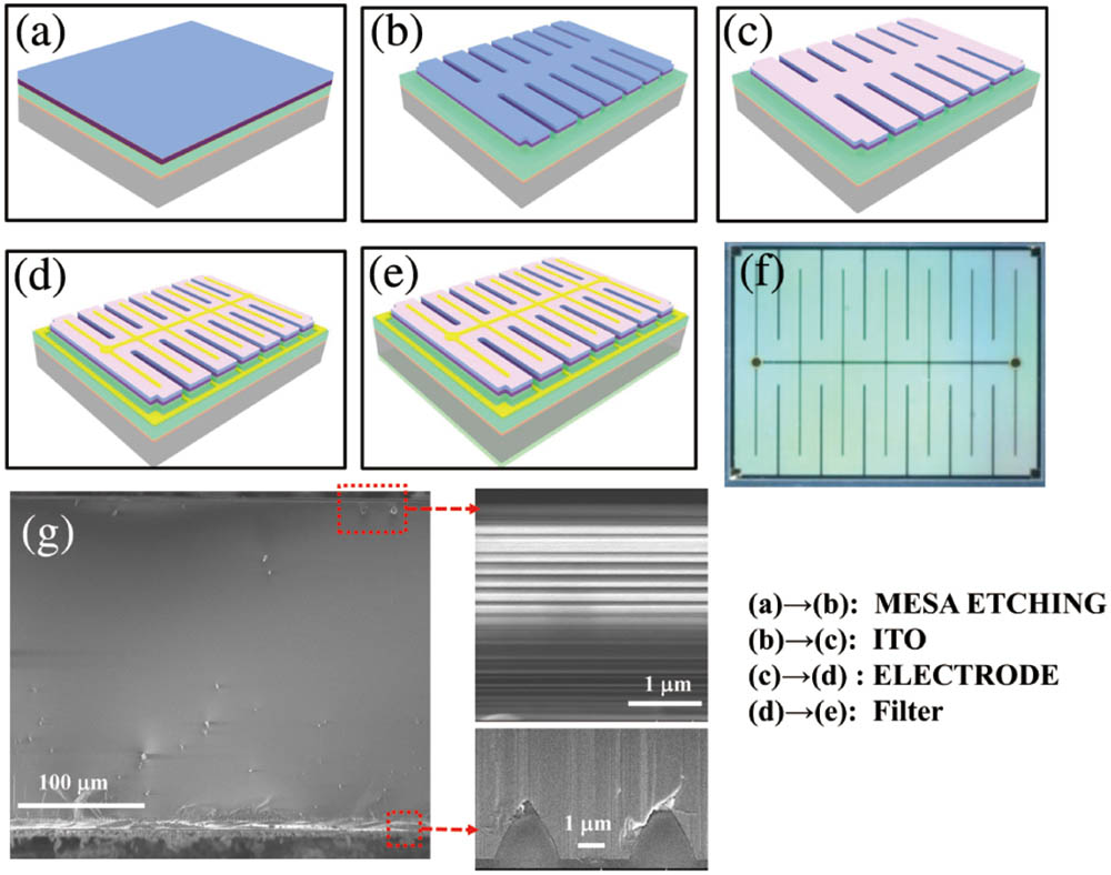
As presented in Fig. 1, similar to our previous work[15–17], the sample is fabricated with the standardized device process including photolithography and inductively coupled plasma (ICP) etching on a 4 inch GaN-sapphire-based GaN. The 6.2-µm-thick epitaxial films consist of an unintentionally doped GaN (u-GaN), Si-doped n-GaN, InGaN/GaN multiple quantum wells (QWs), and Mg-doped p-GaN. For the device fabrication process, a mesa region is defined by photolithography and ICP etching (with a mixture of and ) with a depth of 1.4 µm to expose the n-GaN surface firstly. Deep ICP etching is further carried out to remove epitaxial films totally for device isolation (Step a to b). Then, a 230-nm-thick transparent indium tin oxide (ITO) current spreading layer is deposited by sputtering, followed by rapid thermal annealing at 530°C in atmosphere for 7 min (Step b to c). Subsequently, the ITO layer is patterned and etched away to expose the n-GaN with a mixture of . Then the Ni/Al/Ti/Pt/Ti/Pt/Au/Ti/Pt/Ti followed by a metal lift-off process and rapid thermal annealing metal stacks are deposited on the n-GaN and ITO surfaces (850°C, 30 s in condition) (Step c to d). To protect the device, a 1-µm-thick layer is deposited to the wafer by plasma enhanced chemical vapor deposition. Finally, the sapphire substrate is lapped and polished down to 200 µm, and the chips are diced by ultraviolet nanosecond laser micromachining.
Sign up for Chinese Optics Letters TOC. Get the latest issue of Chinese Optics Letters delivered right to you!Sign up now
![]()
Figure 1.Schematic diagram of sample preparation process: mesa the sample to expose the n-GaN surface (Step a to b), deposit of the ITO film (Step b to c), deposit of the electron (Step c to d), and deposit of the SiO2 and TiO2 filter layer in the back of the device (Step d to e). (f) CCD image of actual sample. (g) Cross SEM of the LED with a filter, the enlarged area shows the filter layer on the top and bottom pattern structure.
After the fabrication of the LED, by utilization of the optical thin film coater, a 2.3-µm-thick distributed Bragg reflector (DBR) containing 36 pairs of is deposited on the bottom sapphire surface of the LED (Step d to e). In order to achieve the desired reflectance spectra, an inhomogeneous thickness distribution of the pair is required. Finally, a square LED with a size of was prepared [shown in Fig. 1(e)]. A comb-like surface electrode was introduced into the device to improve the current uniformity.
3. Results and Discussion
The CCD image of the final device is presented in Fig. 1(f). An interdigital electrode was used to drive it. Details of the inside morphology and structural characteristics were tested and are presented in Fig. 1(g). It shows a typical cross-sectional scanning electron microscope (SEM) image of the patterned sapphire substrate. From bottom to top, there is the p-GaN layer, QWs layer, n-GaN layer, patterned sapphire substrate, and filter layer. Details of the grown filter layer in the top right corner of Fig. 1(g) indicate that the filter is a 36 layer multi-structure with thickness in the region of 30–150 nm. With this design, a long pass filter with a cutoff wavelength of 550 nm is achieved (presented in Fig. S1 of Supplementary Material). Enlarged results for the bottom pattern of the samples in the lower right corner of Fig. 1(g) show that the device has a “triangular pattern” with period of about 2.32 µm and 2.2 µm to balance the lattice mismatch between GaN and sapphire[18,19].
The current-voltage (I-V) characteristic of the diode is characterized using an Agilent B1500A semiconductor device analyzer, and electroluminescence (EL) properties were recorded with a fiber optic spectrometer (Ocean Optics USB 2000+). The measured I-V curve is shown in Fig. 2(c); it shows a turn on voltage of 2.4 V. The integrated EL intensities of the diode of different structures increase with the increasing injection current in Figs. 2(a) and 2(b), and the dominant EL peak is measured at approximately 470.3 nm and FWHM of 19.3 nm at an injection current of 5 mA of the sample with a filter. Compared to our previously reported work with normal LEDs[20], the device presents a red shifted central wavelength and similar turn on voltage. More interestingly, the back filter has no obvious influence on the EL properties (I-V or peak wavelength) of the device. But, it highly reduces the light output of the device in the backside. As inset in Fig. 2(a) shows, light emission from the backside nearly can be ignored. We also observed the EL spectra of the sample without a filter in Fig. 2(b), where the light emission of the back and front is nearly in the same scale in strength. Detailed information in this case can be seen in Fig. S2 of Supplementary Material. External quantum efficiency (EQE) measurement of the chip with or without a filter was done with the integrating sphere method. During the experiment, an LED chip was put inside the integrating sphere, two power sources (Keithley 2410) were used to drive the device, and the Labsphere system (CDS 2600) was used to collect the overall luminous flux of the device under certain driven power. The calculated EQE in Figs. 2(d) and 2(e) indicates that the light output efficiency is about 45.9% for the sample without a filter, and it is decreased to 27.68% for the sample with a filter.
![]()
Figure 2.EL spectra of GaN LED (a) with or (b) without a filter. The inset shows the EL spectra of the device measured from the backside. (c) I-V curve of the LED, inset shows the CCD image of the device under electrical drive. EQE measurements and CIE chromaticity diagram of GaN LED (d) with or (e) without a filter.
To further demonstrate the optical properties of the GaN LED with a filter, reflection spectral characterizations of the devices are performed by using the angle-resolved micro-reflection measurement system with a setup similar to our previous work[21–23]. The measured reflection spectra of LEDs with or without filters are presented in Fig. S3 of Supplementary Material. For samples without a filter [Fig. S3(a) in Supplementary Material], the excitation source is in the region from 400 to 700 nm, the output color is blue, and the reflectance is slightly low (below 15 %). While for the samples with a filter on the back in Fig. S3(b) in Supplementary Material, the output color is red centered at 550 nm with reflectance nearly equal to one, and it becomes blue for the wavelength above 550 nm. All of the samples show relatively friendly angle correlation because our LED is a standard plane structure, which is very good for the application in fluorescence and imaging systems. Details for the reflection spectra under a perpendicular incidence are presented in Fig. 3(d). As can be seen, the filter will block input light with wavelength below 550 nm, and the sample without a filter shows poor reflection properties.
![]()
Figure 3.(a) Principle and experiment setup for fluorescence spectra of the LED device with a filter. (b) Current related fluorescence spectra of dye excited by a blue LED with a filter (collected on the backside). (c) Characteristic spectrum of fluorescence spectra in dye coated samples excited by blue LEDs with or without a filter. (d) Reflection spectrum at perpendicular incidence of GaN LEDs.
As mentioned in the introduction section, an important strategy for simplifying fluorescence imaging is to reduce the intermediate BS mirror to simplify the device structure[24]. To demonstrate the application of our LED with a filter in the fluorescence detection system, a fluorescence spectrum acquisition experiment was performed. During this process, commercial fluorescent material, (Eu, Dy), was used as the probe molecule. Photoluminescence (PL) details of the probe molecule can be seen in Fig. S4 of Supplementary Material. As it shows on the right side of Fig. 3(a), dye with a central emission wavelength near 600 nm was chosen as the probe molecule, and the LED with a filter was used as the light source. As is presented in the inset of Fig. 3(a), the probe molecule was dropped onto the LED on the front face and an optical fiber on the back of the device to receive the fluorescence signal. The results are presented in Fig. 3(b), where only the emission of probe materials was observed. Most of the light emission of the source will be blocked. The mechanism is shown on the left of Fig. 3(a), and light of the LED passes away from the front side of the device. The nearby fluorescent dye will be excited by the emission of the LED (emission peak ) and will obtain reflected light with the emission peak . This light will return and pass through the whole device. Due to the fact that the cutoff wavelength is 550 nm, the light wavelength below 550 nm will be blocked, and then only light emission of the dye can be collected by the detector. As shown in Fig. 3(c), only the LED with a filter can realize these results.
More interestingly, the LED with a filter can also be used as the light source to realize fluorescence imaging. As demonstrated in Fig. 4, a solid word of “N J U P T” was written by the dye on a substrate. With the help of an object-camera system, the word “N J U P T” was recorded and presented in the personal computer (PC) side one by one when we push the substrate gradually. To make this process more clear, a recording movie is given as video supporting materials. Visualization 1 indicates the imaging process in large scale, and the enlarged results are shown in Visualization 2. Clearly, the characters “N J U P T” are presented. Compared with the normal imaging system, our design can reduce the semi-reflection mirror.
![]()
Figure 4.Demonstration of fluorescence image and results for display of “N J U P T.”
4. Conclusion
In summary, filter integrated multiple-QW III-nitride diode emitting was fabricated with a standard semiconductor process. Experimental results indicate that the device shows blue emission at 470.3 nm and angle-free long pass properties with a cutoff wavelength of 550 nm. Then, it was used to establish a fluorescence spectral detection or imaging system, which is extended to realize fluorescence spectral imaging without an extra filter and semi-reflection mirror. Clear spectra of the dye probe and words such as “N J U P T” were demonstrated. Our design opens up a promising platform for the semi-reflection mirror-free imaging and can be used in smart and mini optical imaging systems.
References
[1] M. Tsunoda. Recent advances in methods for the analysis of catecholamines and their metabolites. Anal. Bioanal. Chem., 386, 506(2006).
[2] S. Fan, G. Zhang, G. H. Dennison, N. FitzGerald, P. L. Burn, I. R. Gentle, P. E. Shaw. Challenges in fluorescence detection of chemical warfare agent vapors using solid-state films. Adv. Mater., 32, 1905785(2020).
[3] H. C. Zhang, Y.-M. Guo. Advances of carbon quantum dots for fluorescence turn-on detection of reductive small biomolecules. Chinese J. Anal. Chem., 49, 14(2021).
[4] Z. Bi, Y. Zhang, S. Zhang, L. Wang, E. Gu, Z. Tian. A handheld miniature ultraviolet LED fluorescence detection spectrometer. J. Appl. Spectrosc., 86, 538(2019).
[5] J. Mazina, A. Spiljova, M. Vaher, M. Kaljurand, M. Kulp. A rapid capillary electrophoresis method with LED-induced native fluorescence detection for the analysis of cannabinoids in oral fluid. Anal. Methods, 7, 7741(2015).
[6] J. A. Chediak, Z. S. Luo, J. G. Seo, N. Cheung, L. P. Lee, T. D. Sands. Heterogeneous integration of CdS filters with GaN LEDs for fluorescence detection microsystems. Sensors. Actuat. A, 111, 1(2004).
[7] M. L. Y. Sin, J. Gao, J. C. Liao, P. K. Wong. System integration-a major step toward lab on a chip. J. Biol. Eng., 5, 6(2011).
[8] G. Ryu, J. Huang, O. Hofmann, C. A. Walshe, J. Y. Y. Sze, G. D. McClean, A. Mosley, S. J. Rattle, J. C. deMello, A. J. deMello, D. D. C. Bradley. Highly sensitive fluorescence detection system for microfluidic lab-on-a-chip. Lab Chip, 11, 1664(2011).
[9] S. Joo, K. H. Kim, H. C. Kim, T. D. Chung. A portable microfluidic flow cytometer based on simultaneous detection of impedance and fluorescence. Biosens. Bioelectron., 25, 1509(2010).
[10] F. Lefevre, P. Juneau, R. Izquierdo. Integration of fluorescence sensors using organic optoelectronic components for microfluidic platform. Sensors. Actuat. B, 221, 1314(2015).
[11] P. K. Buah-Bassuah, H. M. von Bergmann, E. T. Tatchie, C. M. Steenkamp. A portable fibre-probe ultraviolet light emitting diode (LED) induced fluorescence detection system. Meas. Sci. Technol., 19, 025601(2008).
[12] L. Novak, P. Neuzil, J. Pipper, Y. Zhang, S. Lee. An integrated fluorescence detection system for lab-on-a-chip applications. Lab Chip, 7, 27(2007).
[13] S. Xue, K. Uchiyama, H.-F. Li. Determination of ammonium on an integrated microchip with LED-induced fluorescence detection. J. Environ. Sci., 24, 564(2012).
[14] M. Yao, G. Shah, J. Fang. Highly sensitive and miniaturized fluorescence detection system with an autonomous capillary fluid manipulation chip. Micromachines, 3, 462(2012).
[15] Z. Shi, X. Li, G. Zhu, Z. Wang, P. Gruenberg, H. Zhu, Y. Wang. Characteristics of GaN based LED fabricated on a GaN-on-silicon platform. Appl. Phys. Express, 7, 082102(2014).
[16] X. Li, Y. Wang, K. Hane, Z. Shi, J. Yan. GaN-based integrated photonics chip with suspended LED and waveguide. Opt. Commun., 415, 43(2018).
[17] W. Cai, Y. Yang, X. Gao, J. Yuan, W. Yuan, H. Zhu, Y. Wang. On chip integration of suspended InGaN/GaN multiple quantum well devices with versatile functionalities. Opt. Express, 24, 6004(2016).
[18] H. Y. Shin, S. K. Kwon, Y. I. Chang, M. J. Cho, K. H. Park. Reducing dislocation density in GaN films using a cone shaped patterned sapphire substrate. J. Cryst. Growth, 311, 4167(2009).
[19] S. S. Pasayat, C. Gupta, M. S. Wong, Y. Wang, S. Nakamura, S. P. Denbaars, S. Keller, U. K. Mishra. Growth of strain-relaxed InGaN on micrometer sized patterned compliant GaN pseudo substrates. Appl. Phys. Lett., 116, 111101(2020).
[20] L. Wang, X. Li, X. Gao, B. Jia, Q. Guan, Z. Ye, K. Fu, R. Jin, Y. Wang. Asymmetric optics links using monolithic III-nitride diodes. Opt. Lett., 46, 376(2021).
[21] X. Shen, W. Wang, X. Gao, Q. Chuan, Z. Shi, Y. Wang. Membrane-type polarization controlled color filters on silicon substrate. Opt. Laser. Technol., 105, 4(2018).
[22] W. Wang, G. Zhu, Q. Liu, X. Li, T. Sa, X. Fang, H. Zhu, Y. Wang. Angle and polarization dependent spectral characteristics of circular grating filters. Opt. Express, 24, 11033(2016).
[23] W. Wang, X. Li, J. Luo, W. Cai, X. Gao, G. Zhu, Y. Wang. Ultracompact multilayer Fabry Perot filter deposited in a micropit. J. Light. Technol., 35, 4973(2017).
[24] Y. L. Qin, X. L. Luan, L. J. Bi, Z. Lue, Y. Q. Sheng, G. Somesfalean, C. N. Zhou, Z. G. Zhang. Real-time detection of dental calculus by blue-LED-induced fluorescence spectroscopy. J. Photochem. Photobiol. B, 87, 88(2007).

Set citation alerts for the article
Please enter your email address
© Copyright 2018-2021 | Chinese Laser Press. All Rights Reserved 沪ICP备15018463号-20