
Yan Zhou, Minghui Hong. Formation of a three-dimensional bottle beam via an engineered microsphere[J]. Photonics Research, 2021, 9(8): 1598
- Photonics Research
- Vol. 9, Issue 8, 1598 (2021)
Abstract
1. INTRODUCTION
Optically trapping and translating particles using focused laser beams has become the technology for non-contact manipulation of microscopic objects, with extensive impacts on applications ranging from optics, thermodynamics, biology, and atomic physics [1–8]. Conventional optical tweezers use high-numerical-aperture () lenses to generate a stable gradient trapping potential [3], which are bulky and of high cost; they also suffer from a lack of flexibility and integrated ability, poor remote operating capability, and demand for large-volume infrastructure. As an alternative, optical fiber-based tweezers have also been developed in the form of paired and counter-aligned fibers or a tapered/patterned fiber [9–13], but they offer limited control over the light field, and yet they are not suitable for large-scale integration. Another field of approaches is on-chip devices, including planar photonic devices, such as optical waveguides [14–16], plasmonic structures [17–19], and optical resonators [20–22], and has been proposed for on-chip trapping. These devices utilize evanescent waves to produce the optical-gradient potential, which only allows particle manipulation in two dimensions at immediate proximity of the chip surface due to the stringent decay length of evanescent fields.
Stable and robust optical trapping demands a strong gradient force along three spatial directions () to provide a sufficient trapping force in the radial direction and counterbalance the scattering force along the axial direction. One structured light beam called the “bottle beam” contains volumes of low (zero) intensity surrounded by the high-intensity regions, providing efficient means for the 3D particle localization and controllable displacement [23–27]. Such beams can be generated, e.g., by the superposition of oppositely propagating optical vortex beams [25] or inside the focal volume of a lens with a controlled spherical aberration [26]. Generation of such beam structures usually relies on a combination of complex optics [24,25]. In many cases, the resulted optics traps are of sizes from the micrometer to millimeter range [26,27], so one trap can contain a cluster of micro/nanoparticles with Brownian motions, which is not favored for isolated trapping. As such, the generation of the gradient optical trap from specially designed miniaturized optics can be a good alternative approach. Transparent microspheres are a class of refractive micro-optics possessing elegant light focusing with low loss and have proved to achieve various performances in nano-patterning and nano-imaging [28–31]. With the help of engineered nanostructures on the microsphere, further configuration of the focused light field can be achieved to generate structured or tailored beams [32–37].
In this paper, we propose and demonstrate a novel design of micro-optics for optical trapping, whose functionality is based on the refractive microsphere decorated with spatially variant diffractive patterns, to generate a structured beam with a 3D void space as the gradient optical trap, or an “optical bottle.” The spatially variant diffraction pattern is made from segmented annular rings taken from Fresnel zone plate (FZP) designs. Unlike conventional FZP patterns, each segment ring has its center of curvature dislocated from the optical axis in the transverse plane (perpendicular to the light propagation axis). Region-selective manipulation of light, from each part of the hybrid diffraction patterns, couples with the strong light focusing of the microsphere body and forms a bottle beam with near or sub-wavelength void space as the optical trap. This novel design of micro-optics is ideally suited for integrated optical tweezers benefiting from several unique features. First, this design enables the precise positioning of the trap location in the 3D region above the micro-optics and facile adaptations of the trapping potential. Second, compared to other planar devices used for free-space outcoupling, such as diffractive gratings, plasmonic scatterers, and metasurfaces, refractive-based micro-optics offers excellent optical efficiency and broadband operation. The high efficiency enables a low trapping threshold power, whereas the large spectral bandwidth is favored for fluorescence or Raman excitation. Micro-optics can be seamlessly integrated with on-chip waveguides and interfaced with photonic integrated circuits to include new functionalities, such as dynamic tuning of optical traps. In the following, we will present the design, fabrication, and characterization of two embodiments of the engineered microspheres.
Sign up for Photonics Research TOC. Get the latest issue of Photonics Research delivered right to you!Sign up now
2. DESIGN AND METHOD
In this paper, the core idea of this design is to incorporate the focusing of light by the refractive microsphere body and light manipulation by the diffractive pattern on the truncated surface of the engineered microsphere. The resulted optical bottle beam comprises two axial foci and a center-hollowed region connecting the two focal beams, as seen in Fig. 1(a). The two foci are generated from the diffraction pattern as designed, while the interconnecting region of the light field is formed from two sources. The first source is the deliberately uncompensated spherical aberration of the truncated microsphere, and the second source is attributed to the centers of curvature of all segment zones being dislocated from the optical axis.
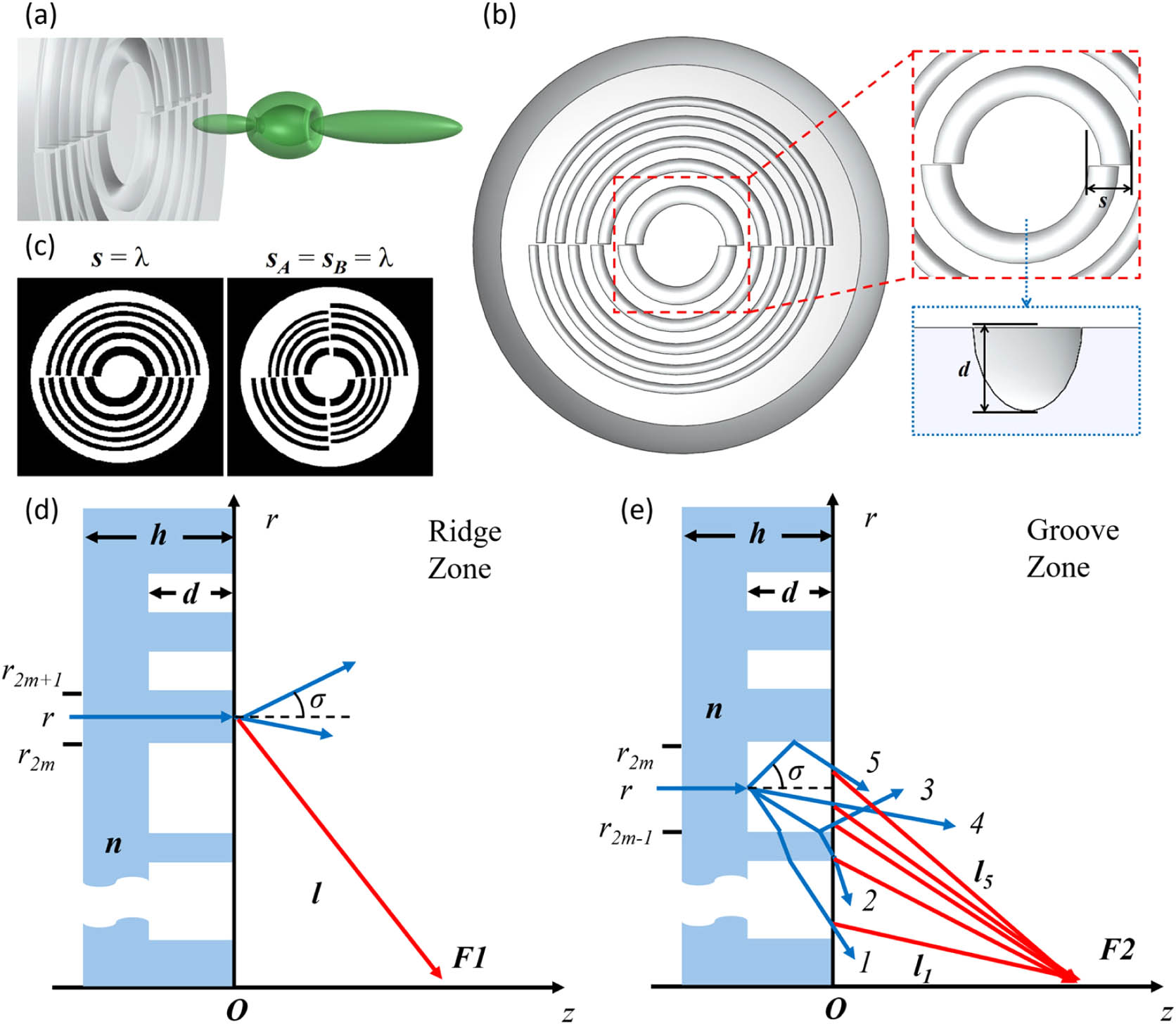
Figure 1.Conceptual design of engineered microsphere patterned with the segmented Fresnel annular zones. (a) 3D sketch of optical bottle beam (green) generated from the engineered microsphere. (b) Schematic sketch of the two-segment zone design engineered microsphere,
For microspheres with diameters larger than , they exhibit substantial spherical aberration when light propagation is not restricted to a small fraction of its cross section. In the geometric optics regime, for positive spherical aberration, the light rays close to the optical axis intersect it near the paraxial focus position. As the ray height at the lens increases, the position of the ray intersection with the optical axis moves farther away from the paraxial focus towards the lens. In a carefully aligned system, the only significant distortion is the one introduced by primary (i.e., third-order) spherical aberration. Assuming plane wave light illuminates from the spherical surface of the truncated microsphere, its Coddington shape and position factors are both equal to . The aberration function , which defines the deviation of the distorted wavefront from the ideal convergent spherical wavefront, can be well approximated by [38]
As described in previous literature, we deal with the monochromatic field whose temporal behavior is described by the factor , which, as usual, is omitted in the subsequent expressions [40]. We also consider the beams with linear polarization, which can be described by the scalar model. Then, the electric fields of a plane wave and a Gaussian beam propagating along the axis are described by the complex amplitude distributions:
The intensity distribution in the focal region of a lens illuminated with a Gaussian beam may be found by evaluating the scalar Debye integral, which is based on the Huygens–Fresnel principle and uses the boundary conditions approximated by the Kirchhoff diffraction theory [40]. The spatial variation of the intensity is then
In the design, several key parameters can directly influence the beam formation. These parameters include the size, material (refractive index) and depth of the truncation of microsphere, wavelength of the coherent illumination light, and diffraction patterns. To be more specific on the diffraction pattern, it is made of segmented phase type FZP annular zones, each segment region has its center of curvature dislocated a distance of from the optical axis, and, within one segment region, all grooves have the same etching depth , as seen in Fig. 1(b). After the segmented annular zones are fabricated on the truncated microsphere, the etched parts are called the groove zones, and the unstructured ring-shape zones in between those grooves are called the ridge zones, as seen in Figs. 1(d) and 1(e). Light emitted from the ridge and groove zones is manipulated in a way that they arrive at different axial positions on the optical axis, forming two distinct focal beams. In our design, the first focal beam (F1), which is located near the exit surface of engineered microsphere, is largely contributed by the ridge zones; the second focal beam (F2) is mainly attributed to the groove zones. Taking as the designed focal length, the FZP zone boundaries are written as
For the incident light passing through each ridge zone, the left side of Fig. 1(d) shows the scattering of transmitted light at the interface of due to the finite size of a ridge. The source field components of the ridge zone are the superposition of scattering light over the range of scattering angle . Assuming that with cylindrical coordinates (, , ) and applying the Rayleigh–Sommerfeld integral, we can obtain the diffraction field of the FZP’s ridge zones [41]:
In this paper, two embodiments of engineered microspheres are studied. One is a two-segment design, and both segmented regions have identical parameters except that they face each other; with a total relative dislocation distance , such embodiment is visually presented in Figs. 1(a)–1(c). The phase transformation introduced by the designed pattern can be defined as
The other is a four-segment asymmetric design containing four segmented regions [Fig. 1(c)], and the four regions can be separated into two pairs of opposite regions, namely, pairs and . Each opposite pair of regions has the same FZP design, while neighboring regions are of different parameters. The phase transformation introduced by this design can be defined as
The vectorial light field is then simulated using a finite-difference time-domain (FDTD) solver (Lumerical FDTD). The truncated dielectric microsphere is set to face the illumination light with its spherical side surface, thus the shadow side surface is flat and decorated with the designed etch patterns. The microsphere used is set as borosilicate glass ( at 589 nm). As in the experimental setup, the laser beam used has a beam diameter () much larger than the microsphere (), quasi-plane wave approximation is applied, and the illumination source is set to be a linearly polarized plane wave (wavelength of 532 nm). The boundary condition in the FDTD region is set to be perfectly matched layers (PMLs), and a mesh size of is applied within the entire simulation region.
As seen in Fig. 2, simulated Poynting vector distributions and 2D plots show the collective effect of manipulated beams from all engineered regions to form a “bottle beam.” By using a two-segment design with , where , an optical trap in the “bottle beam” is generated with sub-wavelength dimensions in both axial and transverse directions. The dimensions are determined by the direction with the lowest optical potentials. If the peak field intensity in the transverse direction, , is smaller than that for any of the two foci located along the axial direction, , the criterion of optical trap size applies for all directions inside the 3D trap region. This is because the particle trapping in a 3D space relies on the lowest optical potential barrier around it, which in turn determines the power threshold of the laser beam. As expected from the spatially separate patterned regions, “twisted” beams are obvious from the Poynting vector plot at the first focus [Fig. 2(f)]. As the beams continue to propagate, their twisting is still easy to be identified at an observation plane in the optical trap region [Fig. 2(e)]. When light propagates further, beam interference occurs, and thus the beam twisting becomes less remarkable when they meet again at the optical axis to form the second focus, as seen in Fig. 2(d).
![]()
Figure 2.“Bottle beam” generation via a two-segment design engineered microsphere from the view of Poynting vector distributions. (a) A zoomed view of the 3D optical trap with estimated axial and transverse dimensions, which are taken from the square and enclosed region in (b)
Similar to Fig. 2, simulated Poynting vector distributions and 2D plots in Fig. 3 show the “bottle beam” formation from all patterned regions of a four-segment engineered microsphere with . Again, a “bottle beam” is generated with an optical trap of sub-wavelength dimensions in both the axial and transverse directions. Obvious “beam twisting” is observed at the first focus [Fig. 3(f)]. At an observation plane in the optical trap region, beam twisting is still discernible by looking at the Poynting vector distribution [Fig. 3(e)]. However, compared to Fig. 2(e), Poynting vectors around the optical null region possess significantly smaller amplitude variations. At this plane, such amplitude variations are mitigated due to partial interference of light beams emerging from the four smaller spatially variant segmented regions with alternate parameters. When light propagates further, beam interference occurs, and thus the beam twisting becomes less remarkable when they meet again at the optical axis to form the second focus, as seen in Fig. 3(d).
![]()
Figure 3.“Bottle beam” generation via a four-segment design engineered microsphere from the view of Poynting vector distributions. (a) A zoomed view of the 3D optical trap with estimated axial and transverse dimensions, which are taken from the square and enclosed region in (b)
Figure 4 shows a detailed insight by checking phase distributions at the same observation plane from the exit surface for both two- and four-segment designs. For the two-segment case, the mutually dislocated regions act as two sources of manipulated light beams. From and component phase distributions in the upper row of Fig. 3, the phase origin from two beam sources is still identified near the optical axis. As for the four-segment design, it is clear to see that it offers E-field phase singularities in transverse directions, enabling a “3D pocket” with more uniform intensity distributions in transverse planes. Both the component phase maps indicate the spiral-like propagation of beam vectors along the optical axis, while the four-segment design (lower row) results in a narrower distribution of the longitudinal component.
![]()
Figure 4.Phase mapping for the designs at the same observation
To conduct light field distribution characterization, borosilicate glass microspheres (Thermal Fischer, diameter ) are truncated to become hyper-hemispheres using a focused ion beam (FIB) system (GAIA, TESCAN). The two designed patterns (two- and four-segment) are etched on the flat surfaces of the truncated microspheres using the same FIB system. The radius of curvature for the unstructured surface of the Fresnel zone microspheres (FZMS) is . Each of the fabricated engineered microspheres is located within a mesh on a copper transmission electron microscopy (TEM) grid (Ted Pella, thickness ), with its lower waist mechanically held and supported during all experiments. During the FIB fabrication, the depth of truncation of the microsphere is regularly monitored by measuring the radius of the milled flat surface. The value of can be calculated using simple trigonometry , where is the radius of the original microsphere. The effect of the ratio on the beam formation and the optimization process has been discussed in our previous work [36]. To monitor groove depths, before each sample fabrication, a testing sample (truncated microsphere) of the same material is used to adjust FIB parameters to etch grooves with a certain designed depth according to simulation settings.
3. RESULTS AND DISCUSSION
The microspheres engineered by FIB as seen in Figs. 5 and 6 are characterized with the experimental setup as described in the previous literatures using a commercial optical microscope system (Nikon Eclipse Ni-E) [35–37]. The linearly polarized illumination beam is from a laser source (532 nm, MGL-FN-532, CNI Lasers) with a fixed controller voltage of 0.23 V in all experiments. The laser beam is directed to the spherical side of the engineered microspheres, is focused by the microsphere, and exits from the patterned side to generate “bottle beams” along the optical axis. Fabricated microspheres are observed under a scanning electron microscope (SEM, TESCAN) as well as under an optical microscope (Nikon Eclipse Ni-E) equipped with a high-NA objective lens (, NA 0.9). In Figs. 5 and 6, the characterization results are demonstrated and compared with the simulation results for two- and four-segment designs of the engineered microsphere, respectively.
![]()
Figure 5.Characterization of the fabricated two-segment design microsphere. Images of the fabricated microsphere are taken with (a) SEM and (d) optical microscope. Normalized FDTD-simulated light intensity field
![]()
Figure 6.Characterization of the fabricated four-segment design microsphere. Images of the fabricated microsphere are taken with (a) SEM and (d) optical microscope. Normalized FDTD-simulated light intensity field
Taking the propagation direction or optical axis along the axis, the and planes of measured light field intensity distributions are displayed in Fig. 5. As discussed in Fig. 4, the two-segment design produces two beams traveling in a twisted manner before they meet at the second focus. At the plane of the optical trap region, the trace of two beams is still obvious, and thus the transverse plane intensity distribution is not uniform. As displayed in Fig. 5(b), the cross section of the optical trap possesses an elliptical shape null at the center. Transverse dimensions are in the major axis and 300 nm in the minor axis, respectively. However, for the measured plane result in Fig. 5(c), it seems the optical null from the fabricated sample is less flattening or elliptic, as it displays a dimension of along the major axis and along the minor axis. This might be due to the fact that the hexagonal copper TEM mesh grid holding the microsphere has a smaller diameter () than the microsphere (diameter 22.0 μm). This results in an effectively smaller entrance aperture that partially obstructs some off-axis illumination light. Such a portion of light, if not obstructed, can be directed by the microsphere and its patterned surface to focus close to the optical axis at this observation plane and contributes to the simulated elliptical shape of the optical null. Observing the plane results, the experimentally measured light field in Fig. 5(f) shows most of the key features presented in Fig. 5(e) with similar spatial positions.
Figures 6(a) and 6(d) display the SEM and optical images of the fabricated four-segment design microsphere. From Fig. 3, the four-segment design creates phase nulls in the transverse plane between the two foci. As such, the transverse plane intensity distribution is more uniform within the 3D optical trap region. As demonstrated in Fig. 6(b), the cross section of the optical trap possesses a round-shape null at the center with a diameter of , while the measured plane result in Fig. 6(c) also shows that a round-shape optical null is generated from the four-segment sample, which largely agrees with the simulation. Nevertheless, the actual diameter of the generated optical trap at the same plane is . As mentioned above, the engineered microspheres are sitting on a copper TEM grid with a mesh size () slightly smaller than the microsphere diameter, resulting in an effective entrance aperture to partially restrict off-axis illumination. The enlarged sizes could also be due to background interference with deflected light from neighboring mesh grids. Observing the plane results, the experimentally measured light field in Fig. 6(f) shows most of the key features presented in Fig. 6(e) with similar spatial positions.
Both fabricated samples produce sub-wavelength size optical nulls that can be used to trap nanoparticles in 3D space. For 3D trapping of cold single atoms, a conventional method is to use holography to create bottle beams, in which the smallest trap size achieved is ∼2 μm in the radial direction, and the axial size is about twice that of the radial one [42]. As a comparison, our approach provides even smaller trap dimensions in both the axial and radial directions. However, it can be seen from both figures that in the measured light fields, the 3D void space part has the enclosure light field generally larger in size, and its connection to the two foci in the axial directions is weaker. In this sense, the actual laser power threshold required for trapping a nanoparticle in position is larger than that being designed. One way to improve the experimental condition is to change the holding substrate from metallic mesh grids to a transparent substrate to reduce background interference.
4. CONCLUSIONS
This paper proposes a novel scheme of the engineered microsphere with the segmented regions of diffractive patterns to generate an optical bottle beam with specially manipulated wavevectors under linearly polarized illuminations (wavelength of 532 nm). The emitted light field from the exit surface of the engineered microsphere forms a pair of axially arranged focused beams, and they are connected with a continuous optical field embracing a 3D optical null or void at the center. Such a new design can be executed into different embodiments, two such designs are demonstrated with both simulation and experiment. The two-segment design is simpler, but the intensity field distribution around the optical null is less uniform, while the four-segment design creates a 3D optical trap with more uniform intensity field. This novel scheme paves a way to create new micro-optics for specialized functional light field generation, which can be tuned by changing parametric designs, including the etched groove depth and total relative dislocations of centers of curvature. Further tuning can be possible if more types of diffraction patterns (e.g., photon sieves) are included in the segmented region design. Other than localized 3D optical trapping, this class of design can be used in the applications of structured light illumination microscopy and laser micro-processing.
References
[1] A. Ashkin. Acceleration and trapping of particles by radiation pressure. Phys. Rev. Lett., 24, 156-159(1970).
[2] M. Daly, M. Sergides, S. Nic Chormaic. Optical trapping and manipulation of micrometer and submicrometer particles. Laser Photon. Rev., 9, 309-329(2015).
[3] A. Ashkin, J. M. Dziedzic, J. E. Bjorkholm, S. Chu. Observation of a single-beam gradient force optical trap for dielectric particles. Opt. Lett., 11, 288-290(1986).
[4] K. Dholakia, P. Reece, M. Gu. Optical micromanipulation. Chem. Soc. Rev., 37, 42-55(2008).
[5] J. M. Zhu, X. Q. Zhu, Y. F. Zuo, X. J. Hu, Y. Shi, L. Liang, Y. Yang. Optofluidics: the interaction between light and flowing liquids in integrated devices. Opto-Electron. Adv., 2, 19000701(2019).
[6] W. Liu, D. S. Dong, H. Yang, Q. H. Gong, K. B. Shi. Robust and high-speed rotation control in optical tweezers by using polarization synthesis based on heterodyne interference. Opto-Electron. Adv., 3, 200022(2020).
[7] E. Otte, C. Denz. Optical trapping gets structure: structured light for advanced optical manipulation. Appl. Phys. Rev., 7, 041308(2020).
[8] C. Bradac. Nanoscale optical trapping: a review. Adv. Opt. Mater., 6, 1800005(2018).
[9] A. Constable, J. Kim, J. Mervis, F. Zarinetchi, M. Prentiss. Demonstration of a fiber-optical light-force trap. Opt. Lett., 18, 1867-1869(1993).
[10] C. Liberale, P. Minzioni, F. Bragheri, F. De Angelis, E. Di Fabrizio, I. Cristiani. Miniaturized all-fibre probe for three-dimensional optical trapping and manipulation. Nat. Photonics, 1, 723-727(2007).
[11] Y. Liu, M. Yu. Investigation of inclined dual-fiber optical tweezers for 3D manipulation and force sensing. Opt. Express, 17, 13624-13638(2009).
[12] A. Asadollahbaik, S. Thiele, K. Weber, A. Kumar, J. Drozella, F. Sterl, A. M. Herkommer, H. Giessen, J. Fick. Highly efficient dual-fiber optical trapping with 3D printed diffractive Fresnel lenses. ACS Photon., 7, 88-97(2020).
[13] M. Plidschun, H. Ren, J. Kim, R. Förster, S. A. Maier, M. A. Schmidt. Ultrahigh numerical aperture meta-fibre for flexible optical trapping. Light Sci. Appl., 10, 57(2021).
[14] S. Kawata, T. Tani. Optically driven Mie particles in an evanescent field along a channeled waveguide. Opt. Lett., 21, 1768-1770(1996).
[15] A. H. J. Yang, T. Lerdsuchatawanich, D. Erickson. Forces and transport velocities for a particle in a slot waveguide. Nano Lett., 9, 1182-1188(2009).
[16] S. Yu, J. Lu, V. Ginis, S. Kheifets, S. W. D. Lim, M. Qiu, T. Gu, J. Hu, F. Capasso. On-chip optical tweezers based on freeform optics. Optica, 8, 409-414(2021).
[17] M. L. Juan, M. Righini, R. Quidant. Plasmon nano-optical tweezers. Nat. Photonics, 5, 349-356(2011).
[18] K. B. Crozier. Quo vadis, plasmonic optical tweezers?. Light Sci. Appl., 8, 35(2019).
[19] H. Tan, H. Hu, L. Huang, K. Qian. Plasmonic tweezers for optical manipulation and biomedical applications. Analyst, 145, 5699-5712(2020).
[20] Y. Y. Sun, X. C. Yuan, L. S. Ong, J. Bu, S. W. Zhu, R. Liu. Large-scale optical traps on a chip for optical sorting. Appl. Phys. Lett., 90, 031107(2007).
[21] S. Lin, E. Schonbrun, K. Crozier. Optical manipulation with planar silicon microring resonators. Nano Lett., 10, 2408-2411(2010).
[22] A. Krishnan, N. Huang, S.-H. Wu, L. J. Martínez, M. L. Povinelli. Enhanced and selective optical trapping in a slot-graphite photonic crystal. Opt. Express, 24, 23271-23279(2016).
[23] J. Arlt, M. J. Padgett. Generation of a beam with a dark focus surrounded by regions of higher intensity: the optical bottle beam. Opt. Lett., 25, 191-193(2000).
[24] V. G. Shvedov, A. V. Rode, Y. V. Izdebskaya, A. S. Desyatnikov, W. Krolikowski, Y. S. Kivshar. Giant optical manipulation. Phys. Rev. Lett., 105, 118103(2010).
[25] V. G. Shvedov, A. S. Desyatnikov, A. V. Rode, W. Krolikowski, Y. S. Kivshar. Optical guiding of absorbing nanoclusters in air. Opt. Express, 17, 5743-5757(2009).
[26] V. G. Shvedov, C. Hnatovsky, A. V. Rode, W. Krolikowski. Robust trapping and manipulation of airborne particles with a bottle beam. Opt. Express, 19, 17350-17356(2011).
[27] A. Khoroshun, A. Ryazantsev, O. Ryazantsev, S. Sato, Y. Kozawa, J. Masajada, A. Popiołek-Masajada, M. Szatkowski, A. Chernykh, A. Bekshaev. Formation of an optical field with regular singular-skeleton structure by the double-phase-ramp converter. J. Opt., 22, 025603(2020).
[28] L. Chen, Y. Zhou, M. Wu, M. Hong. Remote-mode microsphere nano-imaging: new boundaries for optical microscopes. Opto-Electron. Adv., 1, 170001(2018).
[29] L. Chen, Y. Zhou, Y. Li, M. Hong. Microsphere enhanced optical imaging and patterning: from physics to applications. Appl. Phys. Rev., 6, 021304(2019).
[30] B. S. Luk’yanchuk, Z. Wang, W. Song, M. Hong. Particle on surface: 3D-effects in dry laser cleaning. Appl. Phys. A, 79, 747-751(2004).
[31] B. S. Luk’yanchuk, R. Paniagua-Domínguez, I. V. Minin, O. V. Minin, Z. Wang. Refractive index less than two: photonic nanojets yesterday, today and tomorrow [Invited]. Opt. Mater. Express, 7, 1820-1847(2017).
[32] M. X. Wu, B. J. Huang, R. Chen, Y. Yang, J. F. Wu, R. Ji, X. D. Chen, M. H. Hong. Modulation of photonic jets generated by microspheres decorated with concentric rings. Opt. Express, 23, 20096-20103(2015).
[33] M. Wu, R. Chen, J. Ling, Z. Chen, X. Chen, R. Ji, M. Hong. Creation of a longitudinally polarized photonic jet via an engineered microsphere. Opt. Lett., 42, 1444-1447(2017).
[34] Y. Zhou, H. Gao, J. Teng, X. Luo, M. Hong. Orbital angular momentum generation via a spiral phase microsphere. Opt. Lett., 43, 34-37(2018).
[35] Y. Zhou, R. Ji, J. Teng, M. Hong. Wavelength-tunable focusing via a Fresnel zone microsphere. Opt. Lett., 45, 852-855(2020).
[36] Y. Zhou, R. Ji, J. Teng, M. Hong. Ultralong light focusing via negative axicon microsphere. Eng. Res. Express, 2, 015044(2020).
[37] Y. Zhou, M. Hong. Formation of polarization-dependent optical vortex beams via an engineered microsphere. Opt. Express, 29, 11121-11131(2021).
[38] V. N. Mahajan. Aberration Theory Made Simple(1991).
[39] A. Mikš, J. Novák. Third-order aberration coefficients of a thick lens. Appl. Opt., 51, 7883-7886(2012).
[40] M. Born, E. Wolf. Principles of Optics(1999).
[41] Y. Zhang, H. An, D. Zhang, G. Cui, X. Ruan. Diffraction theory of high numerical aperture subwavelength circular binary phase Fresnel zone plate. Opt. Express, 22, 27425-27436(2014).
[42] D. Barredo, V. Lienhard, P. Scholl, S. de Léséleuc, T. Boulier, A. Browaeys, T. Lahaye. Three-dimensional trapping of individual Rydberg atoms in ponderomotive bottle beam traps. Phys. Rev. Lett., 124, 023201(2020).

Set citation alerts for the article
Please enter your email address
© Copyright 2018-2021 | Chinese Laser Press. All Rights Reserved 沪ICP备15018463号-20