Abstract
Epitaxial quantum dots formed by III–V compound semiconductors are excellent sources of non-classical photons, creating single photons and entangled multi-photon states on demand. Their semiconductor nature allows for a straightforward combination with mature integrated photonic technologies, leading to novel functional devices at the single-photon level. Integrating a quantum dot into a carefully engineered photonic cavity enables control of the radiative decay rate using the Purcell effect and the realization of photon–photon nonlinear gates. In this review, we introduce the basis of epitaxial quantum dots and discuss their applications as non-classical light sources. We highlight two interfaces—one between flying photons and the quantum-dot dipole, and the other between the photons and the spin. We summarize the recent development of integrated photonics and reconfigurable devices that have been combined with quantum dots or are suitable for hybrid integration. Finally, we provide an outlook of employing quantum-dot platforms for practical applications in large-scale quantum computation and the quantum Internet.
Story Video to the Review Article
1 Introduction
Photons are capable of carrying information over long distances. Exploiting photons as quantum bits (qubits), quantum technologies have witnessed substantial advances in quantum networks, quantum simulation, and computation. The quintessential marriage between state-of-the-art nanofabrication techniques and quantum optics gives birth to quantum photonics, which provides essential scalability towards practical quantum applications[1–8]. For decades, single-photon sources relying on the spontaneous parametric downconversion (SPDC) process in nonlinear optical materials have been the workhorse for photonic quantum applications[9–11]. The simultaneous generation of photon pairs makes it possible to herald the generation of one photon with the detection of the other. Despite the ease of operation, SPDC sources are inherently probabilistic, which may become an obstacle when scaling to a large photon number.
Alternatively, two-level emitters can generate single photons on demand: for every trigger, one and only one photon should be created. Epitaxial quantum dots can be simplified as two-level emitters[12,13]. They are nanoscale semiconductor heterostructures, usually of a few nanometers in height and tens of nanometers in diameter. Due to its nanometer size, a quantum dot tightly confines the electrons in space, forming discrete energy levels in the conduction and valence bands. A quantum dot thus mimics an atom in this regard, an “artificial atom.” Every time a conduction-band electron hops down to the valence band and occupies an existing vacancy (a hole), the energy can be released in the form of light—a photon is created. The ability to create a photon, or the radiative lifetime, is related to the optical dipole moment. Since the size of a quantum dot is much larger than that of an atom, the dipole moment is also larger. Thus, the radiative process in a quantum dot is much faster[12–14] (usually on the time scale of a few hundred picoseconds). In a given period of time, a quantum dot creates many more photons than an atom. In fact, the quantum dot is one of the fastest emitters in semiconductors[15].
Unlike atoms for which cooling and trapping techniques must be employed to ensure isolation in position, quantum dots are naturally trapped in the solid state with a fixed location. This feature allows them to be conveniently integrated into a variety of photonic nanostructures by leveraging existing semiconductor fabrication facilities[1,2]. The nanofabrication feasibility makes it possible to engineer the photonic environment of quantum dots[16]. In comparison to the case where the photons escape in all solid angles in unstructured bulk materials, photonic cavities and waveguides surrounding the quantum dot “funnel” the photons into a single confined or propagating optical mode, thereby significantly improving the collection efficiency. A quantum dot embedded in an engineered photonic structure thus provides an almost deterministic dipole–photon interface. In addition, the radiative decay rate of the quantum dot can be enhanced by photonic cavities or waveguides by the Purcell effect, thus increasing the brightness and the photon coherence of the quantum dot for applications as a single-photon source. Moreover, quantum dots are also hosts for single spins. A trapped spin can be in the “up” state, “down” state, or their superposition—it is a stationary quantum bit that possesses quantum information. Coherently manipulating spin states has allowed for a spin–photon interface. These features of the deterministic quantum-dot system have enabled the construction of key quantum components, such as on-demand sources of non-classical photons[14,17–22], nonlinear photon–photon gates[23,24], generators of spin–photon entanglement[25,26], and many more. The quantum-dot platform thus supports a broad range of applications in quantum networks[27] and quantum information processing[2,7].
Sign up for Photonics Insights TOC. Get the latest issue of Photonics Insights delivered right to you!Sign up now
Apart from being embedded into single-mode cavities and waveguides for engineered light–matter interaction, quantum dots can also be integrated with classical photonic components. The well-developed integrated photonic technology[3–6,8] greatly expands the scalability of quantum devices when combined with quantum dots. The flexibility of integration makes quantum dots more appealing compared to many other two-level emitters for solving real-world problems where large resources and stable operations are required; in fact, it has already led to rapid development in quantum photonics. Great efforts have been devoted to improving the performance of photonic devices on the monolithic platform with quantum dots[2,7,16]. Meanwhile, techniques are being improved for the hybrid integration approach, which brings quantum dots to different material systems[4–6,28,29]. For example, quantum dots can be combined with silicon-based photonic systems and superconducting systems, where fabrication technologies are mature, and with the lithium niobate system, which has excellent electro-optical (EO) properties. To construct general-purpose quantum processors, reconfigurability of the photonic circuit can be a major asset[30,31]. Some essential functionalities, such as single-photon routing[32–34] and tunable single-photon spectral filtering[32,35], have already been integrated with quantum dots. Compared to classical photonic circuits, quantum applications set stricter requirements for the performance of photonic components. For example, many quantum photonic applications are sensitive to optical losses. The “no-cloning theorem” demands the insertion loss of photonic devices to be minimized to preserve quantum information. Another requirement lies in constructing reliable photonic devices that work in a cryogenic environment, which is necessary for quantum dots to achieve their best performance.
Over the past two decades, epitaxial quantum dots have been an active research field driven by the flourishing quantum photonic applications[2,7,27]. In this review, we start by outlining the basis of epitaxial quantum dots (including the growth methods, band structures, photoluminescence features, noise processes, etc.) in Section 2. We then provide an overview of epitaxial quantum dots as high-performance sources of non-classical photons in Section 3. Apart from source applications, the deterministic dipole–photon interface in the quantum-dot system leads to intriguing chiral light–matter interaction and nonlinearity at the single-photon level, which is summarized in Section 4. Single spin properties in quantum dots and applications enabled by the spin–photon interface are reviewed in Section 5. The integration of quantum dots into various photonic components opens up new possibilities in building a multi-purpose quantum processor, where device reconfigurability is generally required. In Section 6, we focus on the recent development of reconfigurable quantum photonic integrated circuits (QPICs), which are compatible with quantum dots. Potential applications of quantum-dot-based devices in the future quantum Internet and quantum information processing are presented in Section 7 and Section 8, respectively. As an outlook, foreseeable challenges in quantum-dot technologies are summarized in Section 9, including source efficiency, photon indistinguishability, ensemble inhomogeneity, scalable integration, and spin coherence. We also provide an outlook of exciting future possibilities of quantum dots, including exploring basic physics in quantum optics.
2 Epitaxial Quantum Dots
Quantum dots are formed spontaneously during in situ epitaxial growth, a self-assembly process. For high-quality quantum dots, ultrapure materials must be used in the self-assembly, where defects and impurity levels are well suppressed. The self-assembly of quantum dots usually takes place in a molecular beam epitaxy (MBE) chamber, which offers both the requisite cleanness of growth conditions (ultra-high vacuum) and exquisite control of growth parameters. Exquisite growth control allows various growth techniques to be adopted and optimized for the self-assembly of quantum dots. Here, we focus on quantum dots in III–V semiconductors and outline some widely used growth methods.
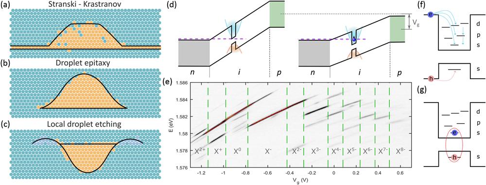
Indium gallium arsenide (InGaAs) quantum dots—smaller-bandgap In(Ga)As nanoislands surrounded by a larger-bandgap GaAs matrix—are a highly established quantum-dot system that has benefited from more than 20 years of development. InGaAs quantum dots, along with some others (e.g., InAs quantum dots in an InP matrix), can be fabricated using the Stranski–Krastanov (SK) method. SK growth relies on a lattice mismatch between two semiconductor materials, e.g., between GaAs and InAs. Due to the lattice mismatch, only a few monolayers[36] (“wetting layer”) of InAs can be deposited on the GaAs surface in a layer-by-layer fashion, after which strain relaxation occurs and the growth continues in the form of nanoisland nucleation. The nanoislands, capped with a GaAs layer to be protected from oxidization and surface states, form optically active quantum dots [Fig. 1(a)].
![Quantum dot heterostructures. (a)–(c) Schematic view of quantum dots grown by the Stranski–Krastranov mode, droplet epitaxy, and local droplet etching, respectively. In the Stranski–Krastranov growth mode, the formation of quantum dots is driven by strain relaxation. Quantum dots are placed on a thin two-dimensional wetting layer and exhibit truncated pyramid shapes[50] after capping. In droplet epitaxy, quantum dots crystallize under the flux of group V materials. The quantum-dot shape tends to be more symmetric compared to that of the Stranski–Krastranov mode, and the wetting layer can be suppressed. For local droplet etching, quantum dots are formed by filling shallow nanoholes. The nanoholes are etched by metal droplets (for example, Al); during the etching process, residual materials (for example, AlAs) diffuse and nucleate around the nanohole, forming a ring structure. (d) Sketch of an n-i-p diode structure hosting a quantum dot. Quantum dot confinements in the conduction and valence bands are highlighted in blue and orange, respectively. On application of an external gate voltage Vg, the quantum dot can be tuned into resonance with Fermi sea level, allowing an electron to tunnel into the quantum dot. (e) Photoluminescence map on varying the external gate voltage Vg shows the locking and tuning of the charge states. The abrupt jump from one charge state to another is a sign of a Coulomb blockade. The shift in emission energy in each charge plateau stems from the quantum-confined Stark effect. In this particular quantum dot, 11 charge states, from X2+ to X8−, are mapped out with a spectrometer. (f), (g) Sketches of energy levels in the conduction band where s-, p-, d-shells are visualized. Here, the diode structure is not taken into consideration. In (f), an electron–hole pair is created by aboveband excitation. The electron is captured by the quantum-dot potential, entering different energy levels. When the electron is in the upper excitonic states, such as p- and d-shells, it is unstable and relaxes to the ground state (s-shell) shortly. In the valence band, energy levels can be complicated. For simplicity, only the heavy-hole ground state is shown. In (g), a resonant laser is used to excite the quantum dot, creating an electron–hole pair at the ground states. Panel reproduced with permission from: (e) Ref. [51] under a Creative Commons license CC BY 4.0.](/Images/icon/loading.gif)
Figure 1.Quantum dot heterostructures. (a)–(c) Schematic view of quantum dots grown by the Stranski–Krastranov mode, droplet epitaxy, and local droplet etching, respectively. In the Stranski–Krastranov growth mode, the formation of quantum dots is driven by strain relaxation. Quantum dots are placed on a thin two-dimensional wetting layer and exhibit truncated pyramid shapes[50] after capping. In droplet epitaxy, quantum dots crystallize under the flux of group V materials. The quantum-dot shape tends to be more symmetric compared to that of the Stranski–Krastranov mode, and the wetting layer can be suppressed. For local droplet etching, quantum dots are formed by filling shallow nanoholes. The nanoholes are etched by metal droplets (for example, Al); during the etching process, residual materials (for example, AlAs) diffuse and nucleate around the nanohole, forming a ring structure. (d) Sketch of an n-i-p diode structure hosting a quantum dot. Quantum dot confinements in the conduction and valence bands are highlighted in blue and orange, respectively. On application of an external gate voltage , the quantum dot can be tuned into resonance with Fermi sea level, allowing an electron to tunnel into the quantum dot. (e) Photoluminescence map on varying the external gate voltage shows the locking and tuning of the charge states. The abrupt jump from one charge state to another is a sign of a Coulomb blockade. The shift in emission energy in each charge plateau stems from the quantum-confined Stark effect. In this particular quantum dot, 11 charge states, from to , are mapped out with a spectrometer. (f), (g) Sketches of energy levels in the conduction band where s-, p-, d-shells are visualized. Here, the diode structure is not taken into consideration. In (f), an electron–hole pair is created by aboveband excitation. The electron is captured by the quantum-dot potential, entering different energy levels. When the electron is in the upper excitonic states, such as p- and d-shells, it is unstable and relaxes to the ground state (s-shell) shortly. In the valence band, energy levels can be complicated. For simplicity, only the heavy-hole ground state is shown. In (g), a resonant laser is used to excite the quantum dot, creating an electron–hole pair at the ground states. Panel reproduced with permission from: (e) Ref. [51] under a Creative Commons license CC BY 4.0.
An alternative bottom-up approach is droplet epitaxy (DE). In DE growth, a group III material (e.g., Ga or Al) is deposited on the surface of the substrate creating nanodroplets[37]. A subsequent annealing process with a supply of group V flux (e.g., As) crystallizes the nanodroplets and turns them into nanoislands [Fig. 1(b)]. Compared with the SK method, nanodroplet formation in DE follows the Volmer–Weber growth mode, irrespective of the lattice mismatch. The DE growth thus offers a wider selection in the material chart (e.g., GaAs/AlGaAs, GaAs/Si, and GaN/AlGaN). A larger variety of material combinations make possible the formation of light-emitting quantum dots in a widespread wavelength range. The DE method can also be tailored for fabricating quantum dots of symmetric shapes or in different substrate orientations[38], e.g., (111)A orientation, and for removal of the wetting layer[39].
Despite its flexibility, DE growth is often performed at moderate temperatures (e.g., 150°C–350°C)[40], making it more prone to defects and impurities, which can consequently lead to poor optical qualities. The recent evolution of the DE method, local droplet etching (LDE), overcomes this hurdle. Similar to DE growth, the LDE method employs metal nanodroplets. After formation, the droplets are annealed at a high substrate temperature (e.g., 600°C) with a low group V flux. The annealing process facilitates the droplet etching process, creating nanoholes beneath the nanodroplets[41]. These nanoholes are then filled with the corresponding quantum-dot materials and then capped with barrier layers [Fig. 1(c)]. GaAs quantum dots in an AlGaAs matrix represent a system where LDE growth has been successfully established[42,43].
Rapid developments in quantum applications post stringent requirements for photons and thus the quantum dot. Although material quality is of key importance, high-quality material itself could not yet guarantee the quantum dot to create high-quality photons that meet the requirements for applications.
On one hand, an exciton confined in the quantum dot interacts with the acoustic phonons in the local environment via deformation potential[44–46]. Such exciton–phonon interaction results in a broad phonon sideband accompanying the zero-phonon line[47]. It also leads to phonon-induced dephasing that broadens the spectral linewidth of the quantum dot (homogeneous broadening), thereby degrading the coherence of the created photons[48,49]. It is essential to work with cryogenic temperatures such that the average thermal occupation of phonons is reduced—most of the quantum-dot experiments rely on cryostats at for photonic applications where phonon occupation is negligible.
On the other hand, noise in semiconductor devices, such as charge noise and spin noise[52], also influences the photons emitted from the quantum dot, causing a spectral fluctuation. Charge noise arises from random electric fields induced by fluctuating charges in the host materials. The electric field alters the frequency of quantum dots via the quantum-confined Stark effect, effectively broadening the spectral linewidth (inhomogeneous broadening). When strong charge noise is present, the frequency of the generated photons wobbles around (Stark effect), and the coherence of the photons gets lost quickly (in the technical term, photons have a short dephasing time). To suppress charge noise, a powerful tool is the Coulomb blockade[12,53,54], an effect that is leveraged to control the tunneling of charge carriers at cryogenic temperatures. For the Coulomb blockade, quantum dots are embedded during growth in a vertical tunneling device where their surrounding matrix materials are doped. Such a tunneling device can be an n-i-p diode[51,55,56] [Fig. 1(d)]: n-doped and p-doped matrix materials are separated by an intrinsic region; quantum dots reside in the intrinsic part of the diode. If the quantum dots stay close to the n-doped matrix, the diode works as an electron tunneling device. The specific design of the diode determines the Fermi sea level of the electrons and holes. A schematic band structure of an electron-tunneling n-i-p diode is shown in Fig. 1(d). If the conduction band of the quantum dot resides above the electron Fermi sea, the electron cannot tunnel into the dot. The dot is thus empty. When an external voltage is applied, the band structure is bent down such that the Fermi sea can align with the lowest conduction-band level of the quantum dot—the dot is filled with an electron. The occupied level then blocks the tunneling of any additional electrons, a Coulomb blockade regime. However, second-order electron tunneling, co-tunneling, can survive. As a larger further bends the band structure, the next electron can tunnel into the dot, and another Coulomb blockade regime starts. This effect is revealed by the abrupt changes in the photoluminescence spectra of a quantum dot [Fig. 1(e)]. The Coulomb blockade locks the charge state within each charge plateau, thus suppressing the charge fluctuation. The suppression of charge fluctuation manifests itself as narrow spectral linewidths of individual quantum dot emission. Near-lifetime-limited linewidths have been demonstrated for both GaAs quantum dots[51,57] and InGaAs quantum dots[55,58,59] with the help of a carefully designed n-i-p diode design at cryogenic temperatures.
The electron wave function in a quantum dot is strongly localized over a large number of lattice sites, where gallium, arsenic, and indium atoms all carry nuclear spins. The nuclear spins interact with the quantum-dot electron via a Fermi-contact hyperfine interaction. In a mean-field approach, the interaction is parameterized as an effective magnetic field, the Overhauser field[60]. Naturally, the nuclear spins in a quantum dot are far from fully polarized; the Overhauser field fluctuates around a mean value[61]. The randomly fluctuating Overhauser field results in spin noise. Spin noise leads to dephasing of quantum-dot single photons; it is also the dominant effect that accounts for the electron-spin dephasing resulting in nanosecond-long -time. Compared to charge noise, which could be efficiently reduced by a diode structure and high-quality materials, suppression of spin noise is usually more difficult: it requires a nuclear-spin cooling technique[62,63] to reduce the fluctuation of the Overhauser field; a larger quantum dot size (more atoms yield a better averaging of nuclear spins) and a homogeneous nuclear-spin environment[64] (all atoms have a nuclear spin of 3/2) can also mitigate the noise.
3 Non-Classical Light Sources
The quantum dot is an excellent two-level emitter that generates pure and identical single photons at a very fast rate. To create a single photon, the quantum dot must be prepared in an excitonic state that contains an electron–hole pair. The excitation process should ideally be triggered such that the photon can be created on demand; the trigger should be fast with respect to the quantum-dot lifetime, in which case, the probability to excite the quantum dot twice within one trigger cycle is minimized (double excitation leads to multi-photon emission events and reduces single-photon purity[65,66]). Common excitation methods rely on either current injection via electrical contacts[67–69] or optical pulses from an external laser source[17–19,57,56,70–72]. In the following, we focus on optical excitation and discuss methods to create non-classical photons.
3.1 Excitation Methods
Early optical excitation attempts use a non-resonant laser pulse—the energy of the laser photons is high with respect to the bandgap of the surrounding matrix material. This method is referred to as above-band(gap) excitation: the laser excites the matrix material, creating charge carriers; the carriers are then randomly trapped into the quantum-dot potential and recombine, resulting in photoluminescence. The spectrum in Fig. 1(e), for instance, is recorded using above-band excitation on a spectrometer. Above-band excitation is rather simple to perform, which leads to its high prevalence for quantum-dot sample characterization. Notwithstanding the popularity, the coherence of the created photons cannot be preserved in the above-band scheme—fast carrier relaxation from upper excitonic states results in time jittering and dephasing [Fig. 1(f)].
When the laser frequency is tuned to the exact energy of the quantum-dot transition, resonant excitation is realized to fully circumvent the time-jitter issue [Fig. 1(g)]. In resonant excitation, no relaxation processes from the upper excitonic levels are involved. Rabi rotations can be achieved using pulsed resonant excitation, and photons created by the quantum dot are at the same frequency as the excitation laser. However, this leads to a technical challenge in the separation of quantum-dot photons from the excitation laser. Different attempts have been made. In the early stage, detection of the quantum-dot signal is evident by a change in the transmission coefficients[73,74]. In this case, photons generated by the quantum dot are mixed with the excitation laser and are thus not suitable for applications such as single-photon sources. Methods allowing to distinguish resonance fluorescence from the laser are subsequently developed. For instance, to eliminate the laser, the layouts of the excitation and the collection paths are designed to be spatially orthogonal to each other[75–77]: the excitation laser is illuminated from the side of the quantum-dot wafer, and the created photons are collected from the top, or vice versa.
Alternatively, one can rely on a cross-polarized confocal scheme[78]: the laser is set to a certain polarization, and photons from the quantum dot are collected in the orthogonal polarization basis. In the cross-polarization scheme, an extinction ratio of up to has been realized[78]—the excitation laser is almost completely eliminated. Due to the high extinction ratio, quantum-dot-based single-photon sources can achieve high single-photon purity.
Albeit fantastic in laser suppression, the cross-polarization approach leads to an intrinsic loss of at least 50% in collection efficiency due to polarization filtering. Such a loss in efficiency is intolerable for practical applications in most quantum technologies. Novel excitation methods are developed to meet the demands from the technology side. Figure 2(a) sketches an excitation concept that takes advantage of a polarized microcavity[20,21], where the fundamental cavity mode is split into two due to geometric birefringence. These two modes are cross-polarized and are slightly offset in frequency. The quantum dot can be selectively coupled to either mode (for example, -mode), yielding a high Purcell factor, whereas coupling to the other mode (-mode) is weak due to detuning. The weakly coupled cavity mode is exploited for excitation, while the strongly coupled cavity mode is used to collect the quantum dot signal. In this case, photons from quantum dots do not experience intrinsic filtering loss.
Figure 2.Creation of non-classical light with individual quantum dots. (a)–(d) Schemes to deterministically prepare a quantum dot for a high upper-level population. In (a), the preparation is mediated by a polarized microcavity. In (b), the excitation is performed with dichromatic laser pulses. (c) Alternating between a high and low Rabi frequency sweeps up the excited state population. (d) In a biexciton cascade, an exciton state can be prepared on demand by combining two-photon excitation and a stimulating pulse. (e)–(h) Microstructures and nanostructures designed to increase the collection efficiency of a quantum-dot single-photon source. (e) Microlens microstructure on top of a bottom DBR. (f) Micropillar cavity where the quantum dot sits between two monolithically grown DBR structures. (g) Tunable microcavity in which the top dielectric mirror is free to move in all three dimensions. (h) Nanobeam waveguide that hosts quantum dots. At the two ends of the waveguide, two grating couplers scatter the quantum dot signal (laser light) into (from) the out-of-plane direction. (i)–(k) Using quantum dots to create entangled photons. (i) Quantum dot embedded in a bullseye cavity as a polarization-entangled photon source. (j) Quantum dot converted to a path-entangled photon source by integration into a glide plane-symmetric photonic crystal waveguide. (k) Scheme to create and verify time–bin entangled photon pairs from a quantum-dot biexciton cascade. Panels reproduced with permission from: (a) Ref. [20] Springer Nature Ltd; (b) Ref. [79] Springer Nature Ltd; (c) Ref. [80] APS; (d) Ref. [81] Springer Nature Ltd; (e) Ref. [82] under a Creative Commons license CC BY 4.0; (f) Ref. [20] Springer Nature Ltd; (g) Ref. [21] Springer Nature Ltd; (h) Ref. [83] under a Creative Commons license CC BY 4.0; (i) Ref. [19] Springer Nature Ltd; (j) Ref. [84] APS; (k) Ref. [85] Optica.
The quantum dot can also be coherently excited using a dichromatic pulsed laser[79,86] [Fig. 2(b)] or relying on a “swing-up” process[80,87] [Fig. 2(c)]. The dichromatic field consists of two sidebands of the same envelope, which are symmetrically detuned with respect to the quantum-dot transition. The phases of the sidebands are locked such that the combination of the sidebands works equivalently as a resonant pulse with a modified envelope[79,86]. The sideband detuning can be sufficiently large () with respect to the quantum-dot linewidth, allowing efficient removal of the laser field using a bandpass spectral filter. In the swing-up scheme, Rabi oscillations with different frequencies are alternated to inverse the population of the two-level system[80,87]. The different Rabi frequencies [Fig. 2(c), red and blue] are achieved using either a frequency-modulated off-resonant laser pulse or two pulses of different strong detunings (the sign of detunings is the same). In the latter case, laser pulses can be red-detuned by several THz from the quantum-dot transition, which allows for simple and efficient removal of the excitation laser. Moreover, by making active use of phonons, the quantum dot can be prepared to the excited state using a slightly off-resonant pulsed laser (blue detuned). The process is referred to as phonon-assisted excitation[72,88–90]; it can be more robust compared to resonant excitation, as it is less sensitive to the drifts in laser power and detuning.
Apart from typical two-level systems (for example, and ), the quantum dot also has a cascade four-level system, involving the biexciton (XX), which can also be exploited for creating non-classical light in a deterministic manner. In the cascade system, two-photon excitation prepares the quantum dot to the biexciton state[70,91]. From the biexciton state, there are two paths decaying to the empty ground state, each through one intermediate exciton state emitting one pair of photons. The two decay paths are similar except for the polarization of emitted photons and a small energy difference between the two exciton states due to the fine-structure splitting (FSS) [Figs. 2(d) and 2(i)]. The emitted photons are in the entangled state . Minimizing the FSS between the two excitons reduces the relative phase in the emitted photon pair and can result in a maximally entangled state. Apart from entangled photons, this cascade system can be tailored to create coherent single photons using a stimulated preparation scheme[81,92–94] [Fig. 2(d)]. Shortly after populating the biexciton, a short laser pulse resonant to one of the two XX-X transitions is applied, selectively transferring the population from the XX state to the X state. The exciton then decays spontaneously, emitting a photon that is separated from the excitation lasers in frequency [Fig. 2(d)]. The separation in frequency allows for efficient removal of the excitation lasers using spectral filters.
3.2 Single-Photon Sources
III–V semiconductor quantum dots are embedded in matrix materials with a high refractive index. For example, the refractive index of GaAs is around 3.5, much higher than that of air and silica. The high refractive index hinders the collection of quantum-dot photons due to total internal reflection at the material interface—a portion of the photons are lost. The photon loss undermines the application of quantum dots as on-demand single-photon sources, and can lead to an error in quantum computational algorithms[95,96]. The photonic environment of a quantum dot must be engineered to reduce photon loss. A simple method is to place a solid-immersion lens (SIL) on top of the quantum-dot sample. Together with a high-numerical-aperture (NA) lens, the SIL enhances collection efficiency while increasing spatial resolution. The gain in collection efficiency depends on the geometry and material parameter (for example, refractive index) of the SIL[97]. Common SIL materials include and GaP, with refractive indices of 2.17 and 3.13 at 950 nm, respectively. Combined with a moderately high-NA collection lens (for example, ), hemispherical and GaP SILs are estimated[98] to increase the collection efficiency by 5 and 11 times (calculated collection efficiencies by the lens are 4.6% and 10.1%, respectively) compared to without an SIL (0.94%). Using 3D-nanoprinted SILs (refractive index of 1.51), the gain in collection efficiency has been experimentally observed, which ranges from 2 to 10 depending on the SIL geometry and the NA of the collection lens[99]. The gain can be further optimized by using materials that match the refractive index of the quantum-dot sample. This motivates the development of a microlens[82,100], a monolithic structure with a hemispherical shape [Fig. 2(e)]. The microlens can be directly fabricated on top of the GaAs quantum-dot sample using electron-beam lithography (EBL) and a cathodoluminescence setup. Moderately high efficiency of up to 40% has been demonstrated using a microlens together with a micro-objective[82,100] [collected by the first lens, assisted by a set of distributed Bragg reflectors (DBRs) as a back mirror], where the purity and indistinguishability of quantum-dot photons can be preserved.
To further boost the collection efficiency and achieve high Purcell enhancement, it is preferable to couple the quantum dot to a single optical mode. Depicted in Figs. 2(f)–2(j), current photonic engineering enables various designs, including micropillars [Fig. 2(f)], tunable open microcavities [Fig. 2(g)], “bullseye” microcavities [circular Bragg gratings, Fig. 2(i)], on-chip nanobeam waveguides [Fig. 2(h)], and photonic-crystal waveguides [Fig. 2(j)], to funnel emission into the collection fiber. The micropillar and the open cavity both use a Fabry–Pérot-type design in a vertical layout where the quantum dot is coupled to the fundamental optical mode. The micropillar has a cylindrical or elliptical cylindrical shape (with a planar footprint of several micrometers), which can be selectively fabricated around a certain quantum dot[20,101–103]. It consists of two sets of DBRs, one above the quantum dot and the other below. In comparison, the open microcavity is assembled with a DBR heterostructure as the bottom mirror; for the top mirror, it is based on a concave mirror in a fused-silica substrate. The bottom DBR with quantum dots embedded is freely movable in all directions by a nano-positioner[21,104]. This tunability opens up the possibility to bring different quantum dots into the resonance of the microcavity mode, compensating for the randomness of both the quantum-dot position and the emission frequency. A cavity can also be defined using in-plane photonic nanostructures. Especially, the periodic appearance of nanoholes and the high-refractive-index bulk material (for example, GaAs) create a photonic crystal with a bandgap. A photonic-crystal cavity (or waveguide) that houses quantum dots is usually formed by removing a few (or a row of) lattices from arrays of regular repeating nanoholes in a nanomembrane. Consequently, the optical density states are strongly modified, and in-plane scattering is suppressed—an in-plane optical mode can be confined in the defect region of a photonic-crystal cavity[13,18,105]. The bullseye cavity is a circular Bragg grating[106,107] on top of a broadband backreflector[19,108] (this can be, for example, a gold mirror or semiconductor DBRs) [Fig. 2(i)]. The circular Bragg grating consists of etched rings with a radial period matching the second-order Bragg condition, scattering the emitted photons in the upward vertical direction. Alternatively, planar waveguides are capable of coupling the emitted photons to a wide bandwidth propagating optical mode. The waveguide can be as simple as a freely suspended beam[83,109] of several hundred nanometers wide [Fig. 2(h)]. Leaving out a row of holes in the trianglar-lattice photonic crystals can also form a waveguide[18,22,84] [Fig. 2(j)]. Such a photonic-crystal waveguide can be highly dispersive, enabling the slow-light effect and enhanced strong light–matter interaction.
Provided an ideal quantum dot where photons are created with unity intrinsic efficiency (that is, ignoring nonradiative decay, blinking, state preparation infidelity, etc.), the collection efficiency quantifies how well a photonic structure funnels quantum-dot photons into a specific output mode. The efficiency should be considered separately for broadband waveguides and for narrowband cavities. In a photonic waveguide, the efficiency is usually characterized by the -factor, which quantifies the ratio of quantum-dot emission into a single-waveguide mode (typically, the fundamental waveguide mode, ) over the total decay rate : . Here, is the decay rate into other modes, and is the Purcell factor[110]. A near-unity -factor has been achieved by suppressing the emission into unwanted guided modes and radiative modes so that in photonic-crystal waveguides is smaller than the radiative rate in bulk[110–112]. For the cavity, the collection efficiency is determined not only by the -factor of the desired cavity mode, but also by the escaping rate of the cavity mode , i.e., . The -factor is further related to the cooperativity () or the Purcell factor () of the cavity by [20,21]. , , and are determined by three rates: the coherent coupling rate () between the emitter and the cavity, the emitter decay rate into non-cavity modes (), and the cavity loss rate (), which consists of the desired photon leakage rate out of the cavity () and the unwanted photon loss rate (), i.e., . The expressions read: and , respectively. For the cavity-based single-photon source, taking , , and , the maximum efficiency is achieved when , in which case the cavity works in the weak coupling regime[21,113].
The efficiency that determines the likelihood of collecting a photon in a collection fiber is further related to the intrinsic quantum efficiency of the emitter, the excited-state preparation efficiency, and the loss along the path, that is, the loss of optical elements and due to fiber coupling. For the photonic microstructures and nanostructures mentioned above, we quote the state-of-the-art , , and values in the content of single-photon generation: with a micropillar cavity, , , and have been achieved[103]; using an open microcavity, a metric of , , and are currently possible[21]. For in-plane structures, one obtains , , and with a bullseye cavity[20]. In a photonic-crystal waveguide, efficiencies and and Purcell factor are achieved independently[22,114]. The current in the waveguide is limited to a maximum of 50% due to the fact that the photons can escape from both sides of the waveguide, which implies that it can be increased by terminating one side of the waveguide[22]. A high Purcell factor has been achieved in a photonic-crystal cavity, albeit a relatively low [18]. Despite promising developments over the past decade, the efficiency of the source still needs to be improved. To this end, it is essential to investigate the quantum dot with near-unity intrinsic quantum efficiency, and to reduce the loss along the way to the collection fiber. The former points to suppressing the nonradiative decay and the coupling to phonons. For instance, well-established InGaAs quantum dots can have a quantum efficiency of [22,115]. The latter involves matching the out-of-plane mode profile to that of the single-mode fiber, a smart design to mitigate loss in semiconductors, and using highly efficient optical elements.
The other metrics for quantum-dot based single-photon sources are the purity and indistinguishability. To spell it out, no more than one photon should be generated at a time; the photons must be identical (indistinguishable) in all aspects. When two pure and indistinguishable photons enter a beam splitter from opposite ports, they coalesce and exit together in one port, a Hong–Ou–Mandel effect. When the photons are not indistinguishable, they create a “mode-mismatch” error in optical quantum computation and simulation algorithms[116]. The purity of the photons is characterized by the Hanbury Brown and Twiss (HBT) effect in an autocorrelation () experiment. For pure single photons, the second-order autocorrelation function at the zero delay is vanishing, . Ideally, the quantum dot can be treated as a two-level emitter, in which case they create pure single photons; thus, photon purity, defined by , is unity. In reality, the purity of quantum-dot photons is affected by the pulse length of the excitation laser[65,66], the excitation method, and how well the excitation laser can be filtered from the quantum-dot photons. With short laser pulses (for example, a couple of picoseconds in pulse width) and efficient filtering of excitation laser pulses, a purity of 99.96% has been achieved[92].
Indistinguishability is directly related to the noise in the semiconductor. Noise can be categorized by its fluctuation time scale; the noise of different frequencies affects the capability of a quantum dot to create identical photons within different delay times. For example, if two photons are created faster than the noise fluctuation, the quantum-dot environment can remain static, and thus the photons are identical. If, however, there is a long delay time between the creation processes of photons, then the indistinguishability tends to be downgraded by the fluctuating noise[58,117,118]. It is therefore hard to create a long string of identical photons because the indistinguishability drops as the delay time grows. It is even more challenging to create identical photons from different quantum dots; in this case, the noise of all frequency bandwidths matters.
Along the frequency chart, phonon dephasing is a fast noise process[18,119] (usually in the GHz range). It affects photon indistinguishability even when the creation delay is short. Charge noise and spin noise are usually slower with respect to the dephasing. They affect the coherence of the photons when the creation delay is long[58,117]. For instance, charge noise lies mostly within the frequency band of in low-noise quantum dots where a diode structure is implemented to suppress the charge noise, while spin noise can have a higher frequency [52]. So far, photons successively created by single quantum dots have been made almost perfectly identical—the indistinguishability[101,120] is near 100%. For a longer creation delay time, for example, of the order of µs, 96% indistinguishability can be maintained using Purcell enhanced InGaAs quantum dots[21,22]. For GaAs quantum dots, 98% indistinguishability[57] has been achieved for a similar delay time.
3.3 Entangled Photon-Pair Sources
The quantum dot can also work as a source of entangled photon pairs. When the biexciton cascade is exploited, a polarization-entangled photon pair is created, provided that the FSS of the neutral exciton () is minimized[19,70,91,121]. As far as the FSS is concerned, quantum dots with symmetric shapes are favored. As discussed in Section 2, a more symmetric morphology can be obtained by DE and LDE growth, for instance, the typical value of of GaAs quantum dots is around 1–2 GHz. Figure 2(i) demonstrates a GaAs quantum dot coupled to a bullseye cavity: with Purcell enhancement (), an entanglement fidelity of 88% has been demonstrated when . The FSS can be further minimized by post-growth tuning methods. The application of multiaxial strain[122–124] or electric field[125] to quantum dots allows for a near-complete erasure of the FSS, . Using strain tuning, 98% entanglement fidelity and 97% concurrence have been achieved[124]. Here, even though the FSS is vanishing, the limitation to concurrence (or entanglement fidelity) likely lies in the optical excitation processes where laser induces an energy splitting to the system by the ac Stark effect[126].
Combining the biexciton cascade system with a photonic waveguide enables the creation of a dual-rail entanglement source[84] [Fig. 2(j)]. The entanglement is transformed from polarization encoding to path encoding via the chiral effect. The chiral effect provides polarization-dependent directionality (see Section 4), guiding circularly polarized photons with opposite helicity () to different paths (path A or B). Likewise, the key is a minimized FSS. The precise positioning of the quantum dot with respect to the photonic waveguide is yet another prerequisite to an operational path-entangled source[84].
Alternatively, the biexciton cascade can be turned into a source of time–bin entangled photons using the simple optical design illustrated in Fig. 2(k). The excitation is composed of an early pulse and a late laser pulse with a relative phase , each of which creates a biexciton–exciton photon pair. The generated photon state, which reads , is analyzed by two post-selected interferometer setups[85,127]. When eliminating the which-path information in the biexciton cascade, the polarization information can be superimposed into time–bin-entangled photons, creating a hyperentanglement[128]. The challenges are two-fold: to minimize FSS and to maintain a stable phase of the interferometers. So far, 81% (polarization) and 87% (time–bin) entanglement fidelities have been achieved for hyperentanglement[128].
4 Deterministic Dipole–Photon Interface in a Quantum Dot
A quantum dot coupled to a single optical mode offers a deterministic dipole–photon interface that allows advanced quantum functionalities, such as a chiral light–matter interaction, and nonlinearity at the single-photon level, to be realized.
4.1 Chiral Light–Matter Interaction
A chiral dipole–photon interface is formed when the coupling between an emitter dipole and a photon depends on the polarization of the dipole () and the propagation direction of the photon. It is a consequence of optical spin–orbit coupling, when the counterpropagating photonic modes have opposite local polarizations[129]. In the ideal situation where an emitter is coupled deterministically to a photonic mode and all decoherence processes are suppressed, the chiral effect manifests itself in two forms. First, the propagation direction of the photons originated from an emitter dipole is locked with the dipole polarization, i.e., a dipole leads to emission into counterpropagating optical modes. Second, the dipole interacts only with the photonic mode in a specific propagation direction. Photons from the opposite propagation direction are not affected by the emitter dipole. The chiral dipole–photon interface has promising potential in applications such as single-photon isolators[104] and single-photon circulators[130,131]; it also provides a paradigm to investigating many-body physics in cascaded quantum systems[132,133].
Photonic nanostructures offer a versatile platform to implement the chiral light–matter interface because they can be engineered to support only one photonic mode and can provide an almost deterministic coupling between the mode and the emitter. In experiments, since the local polarization of the tightly confined photonic mode varies significantly as a function of position[129], the chiral behavior of a quantum-dot dipole strongly depends on its spatial location in the photonic structure. This behavior is also affected by the decoherence processes discussed in Section 3. The degree of chirality can be characterized by the directionality contrast () when considering the emission of two orthogonal dipole transitions into a specific mode (), defined as ( for left-/right-propagating mode), where is the spontaneous emission rate into the -mode from a dipole. Alternatively, it can be described by the directional -factor () that quantifies the fraction of quantum-dot emission into a photonic mode propagating in one direction versus all other modes, which is defined as ( for a dipole). Here, is the spontaneous emission rate of a dipole into unbound modes that leak away from the photonic structure. Directionality contrast and the directional -factor are related, . Up to now, chiral interfaces involving quantum dots have been demonstrated in various on-chip structures including nanobeam waveguides[109], waveguide crossings[134,135], and photonic-crystal waveguides[130,136] [Fig. 3(a)–3(c)], where and directional -factor have been achieved. Recently, a single-photon isolator has been constructed with a quantum dot coupled to a tunable open microcavity, deploying non-reciprocal photon absorption when the system is tuned in situ to operate at [104] [Fig. 3(d)].
Figure 3.Chiral light–matter interaction. Chiral quantum-dot emission in planar photonic structures, including (a) nanobeam waveguide, (b) waveguide crossing, and (c) photonic crystal waveguide. (d) Single-photon isolator with a quantum dot embedded in an open cavity. Topological quantum photonic interfaces in (e) spin-Hall photonic crystal waveguide and (f) side-coupled triangular-shaped resonator consisting of valley-Hall photonic crystal waveguides. Panels reproduced with permission from: (a) Ref. [109] under a Creative Commons license CC BY 4.0; (b) Ref. [135] AIP Publishing LLC; (c) Ref. [137] Springer Nature Ltd; (d) Ref. [104] under a Creative Commons license CC BY 4.0; (e) Ref. [139] AAAS; (f) Ref. [140] Optica.
It should be noted that any aforementioned photonic structure alone is completely reciprocal, and the chiral light–matter interaction (or in the physical term, the spin-momentum locking effect) is position dependent[129,137,138]. In contrast, a topological photonic structure can work as a non-reciprocal device by itself and can provide a location-independent chiral interface to a quantum emitter. For example, a topological waveguide is formed when two photonic structures of different topological phases are closely placed together. A pair of counterpropagating helical edge modes is supported at the interface. An emitter with a dipole at the interface, regardless of its precise spatial location, can couple to, and only to, the edge mode that has the same helicity with respect to the dipole (a chiral effect). Another attractive feature is the topological protection in edge modes: their propagation is supposed to be robust against structural disorders and tight bendings, which is useful for reducing backscattering losses or for the realization of compact devices. As shown in Fig. 3(e), a topological photonic-crystal waveguide is formed between two types of deformed photonic crystals with topologically distinct properties: one with a compressed unit cell (yellow) and the other with an expanded one (blue). Chiral coupling of a quantum dot with helical edge modes in the waveguide has been observed[139]. However, since in this experiment the photonic-crystal waveguide is designed to work at the -point, the coupling efficiency into the waveguide is limited to due to a relatively large decay rate into the free-space radiative mode. By moving the working point from the -point to the K-point, a valley-Hall photonic-crystal waveguide can be constructed[141], where unwanted radiation losses to free space can be greatly suppressed. Figure 3(f) shows such a topological waveguide interfaced with a quantum dot, which demonstrates an averaged directionality contrast of 0.75. Exploiting such a system, a compact traveling-wave resonator in a triangular shape with a circumference of less than 17 µm and a measured Q-factor of 4000 has been demonstrated, where chiral interaction with the quantum dot is also observed [Fig. 3(f)]. For more details on topological quantum photonics, interested readers can refer to Ref. [142] for an overview of recent experimental works and theoretical proposals. Topological photonic structures offer a location-insensitive chiral interface to quantum dots and topological protection of propagating photonic modes from backscattering loss, which can be leveraged for constructing robust, low-loss, and compact devices for chiral quantum photonics.
4.2 Single-Photon Nonlinearity
An appealing functionality of a deterministic dipole–photon interface is strong optical nonlinearity. Such a nonlinear effect is differentiated from classical optical nonlinearity due to its sensitivity at the single-photon level. Typically, photons do not interact with each other because of their bosonic nature. In an optical mode, photon–photon interaction is mediated by the single-photon emitter (such as quantum dots). Strong photon–photon interaction plays an indispensable role in applications such as single-photon switches[23,143], single-photon transistors or photon sorters[24,144], Bell-state analyzers[145], and all-optics quantum logic gates[146,147]. For example, photonic quantum computing can be realized with deterministic one-qubit and two-qubit gates. A controlled-phase gate is an exemplary two-qubit gate, where a -phase shift is acquired by the target qubit conditioned on the state of the control. Early works usually rely on Kerr nonlinearity to realize the controlled-phase functionality. But in this scheme, a high laser power is typically required; since Kerr nonlinearity is a third-order nonlinear effect, the controlled-phase gate usually has low fidelity. Alternatively, nonlinearities on few- or single-photon levels can be achieved by exploiting the intrinsic nonlinearity of a quantum emitter, e.g., a single atom[148–150] or a quantum dot[23,24,144,151–153].
Quantum dots embedded in photonic nanostructures offer an integrated approach to constructing nonlinear quantum devices. Mimicking the prototype atomic system of cavity quantum electrodynamics (cQED), a quantum dot strongly coupled to a photonic-crystal cavity has demonstrated giant single-photon nonlinearity[23,151–153] by exploiting the anharmonicity of the Jaynes–Cummings ladder [Fig. 4(a)]. An ultrafast single-photon switch can be realized using such a system. In the switch, when the control pulse (consisting of a single photon) is present, the signal photon cannot transmit through the cavity: the control photon “switches” off the signal photon[23]. Experimental results have confirmed this behavior, showing increased signal reflection at a frequency detuning corresponding to the transition from to [Fig. 4(a)] and a switch turn-on time of [23]. An alternative approach to realizing single-photon nonlinearity relies on coherent scattering from a quantum dot that deterministically couples with a nanophotonic waveguide[24]. When a few photons in resonance with the quantum dot enter the waveguide, the single-photon component will be reflected by the quantum dot due to destructive interference between the scattered field and the incident field. On the contrary, two-photon and higher-photon components have an increased chance to be transmitted, as schematically illustrated in Fig. 4(b). The zero-delayed autocorrelation functions of the reflected and transmitted laser light show photon anti-bunching [] and bunching [], respectively. The statistics of the higher-photon component in the reflected light has been experimentally studied in a similar system, a quantum dot coupled with a micropillar cavity[144], where third-order autocorrelation functions were measured using a cascaded HBT setup. The measurement yields , much smaller than unity, which indicates that the three-photon component is well suppressed in the reflection [Fig. 4(c)].
Figure 4.Single-photon nonlinearity. (a) A quantum dot strongly coupled to a photonic crystal cavity can work as an ultrafast single-photon switch. (b) A quantum dot in a photonic crystal waveguide works effectively as a single-photon transistor. The single-photon component gets reflected while the two-photon and higher-photon components are transmitted. HBT measurement performed on reflected light using a very weak resonant laser as the input reveals photon antibunching: the reflection has a single-photon character. In transmission, the experiment performed similarly shows photon bunching: the transmission has a multi-photon character. (c) A quantum dot coupled to a micropillar shows a greatly suppressed three-photon component in the reflection. It can be viewed as a filter that removes multi-photon components from single photons. (d) Photon–photon interaction dynamics in a quantum-dot–PhC waveguide system. Panels reproduced with permission from: (a) Ref. [23] Springer Nature Ltd; (b) Ref. [24] under a Creative Commons license CC BY 4.0; (c) Ref. [144] Springer Nature Ltd; (d) Ref. [159] Springer Nature Ltd.
The giant nonlinearity also provides a playground for the investigation of intriguing photon–photon interactions[149,154] such as the formation of the photon bound state[155–157]. Recently, the few-photon scattering matrix[158] and the two-photon interaction dynamics[159] [Fig. 4(d)] have been experimentally explored in a coupled system composed of a quantum dot and a photonic-crystal waveguide. In a two-color experiment, the detuning of the control photon can efficiently shift the emitter resonance for the signal photon on a sub-nanosecond time scale (limited by the emitter lifetime). The ultrafast photon–photon correlation after interaction with the quantum dot has been directly investigated using a fast optical pulse whose duration is comparable to the quantum-dot lifetime. The HBT result maps out the two-photon response of the system [Fig. 4(d)]. The results provide insights into emitter-mediated photon–photon interactions; they also provide a guideline for the construction of high-quality functional quantum nonlinear devices.
Finally, combining the chirality and nonlinearity can enable the creation of linear combinations of N-photon bound states[157,160], which points to a new prospect for novel quantum applications, such as photon sorting, photon-number-resolving detectors, and Bell measurements[145,161,162]. The quantum-dot induced photon–photon interaction may also lead to new opportunities for quantum simulations, for instance, by taking into account anharmonic vibrational effects[7], and in quantum neural networks[163], where the emitter can act as a nonlinear actuator.
5 Single Spins in Quantum Dots
An electron or a hole trapped in the quantum-dot potential enables a spin degree of freedom. In the quantum dot, a large dipole moment allows the carrier spin to be initialized, manipulated, and read out all by optical means. The dipole scatters incident light and creates single photons, establishing a link between the stationary spin and flying photons. This spin–photon interface opens up applications in quantum communication[164] and computation[165].
5.1 Coherent Spin Manipulation
To fully exploit the spin degree of freedom, the quantum dot should be placed in a magnetic field. The magnetic field lifts the degeneracy of the spin states because of the Zeeman effect, forming four energy levels. The strengths and selection rules of the optical transitions in this four-level system depend on the applied magnetic field direction. If the magnetic field is applied along the quantum-dot growth direction (Faraday geometry), only the two spin-preserving transitions, and , are allowed by the selection rules, when assuming that the hole state has a pure heavy-hole character. These two vertical transitions have circularly polarized dipoles. In practice, the diagonal transitions are typically weakly allowed due to either the heavy-hole–light-hole mixing or a small in-plane Overhauser field originated from the fluctuation of nuclear spins. When the magnetic field orthogonal to the growth direction is applied (Voigt geometry), four linearly-polarized dipoles are all optically allowed [refer to the level diagram in Fig. 5(a)].
Figure 5.Spins trapped in quantum dots and a spin–photon interface. (a) Optical means to manipulate a single electron spin trapped in a quantum dot. With an in-plane magnetic field, the trion state forms a four-level system. Typically, two vertical and two diagonal transitions are orthogonal in polarization and similar in oscillator strength. The spin states, , , and their superposition, can be initialized and read out using an optical pulse that is resonant to one of four transitions. Employing a far detuned pulsed laser allows for coherently rotating the spin state. As a function of the power of this rotation laser, a Rabi oscillation between two spin ground states is revealed. (b) Scheme for cooling the nuclear spins surrounding the quantum dot, which reduces the nuclear spin fluctuation, thereby increasing the coherence time of the electron spin. (c) The principal electron spin resonance and its four sidebands are visible when the nuclear spin ensemble is polarized to a state with a very narrow probability distribution. By selectively choosing two-photon detuning, a single nuclear spin can be excited from the nuclear-spin ensemble. (d) Distant spins trapped in two quantum dots are entangled using Raman-scattered photons and an optical interferometer. Joint spin correlations in the spin basis and the rotating basis defined by the superposition are shown in the bottom panel, yielding an average entanglement fidelity of around 62%. Orange: joint spin projection in the population basis; red: projection in the rotated basis of a potential -state; blue: rotated basis, potentially a -state. Panels reproduced with permission from: (a) Ref. [64] under a Creative Commons license CC BY 4.0 and Ref. [166] Springer Nature Ltd; (b) Ref. [62] APS; (c) Ref. [63] AAAS; (d) Ref. [167] APS.
Spin initialization can be achieved by optically driving one transition involving either spin ground state. The optical field “pumps” the population from the specific spin ground state to its spin–flip counterpart. When the driving time is sufficient and the intrinsic spin–flip rate is small, the spin can be initialized with close to unitary fidelity. Likewise, the spin readout can be performed by placing a laser on resonance with the transition involving the spin state of interest. When the spin state is occupied, a photon is scattered, and vice versa. The spin readout fidelity depends on the readout time and decoherence rates of the spin ground state and excited state, together with the system extraction efficiency.
Spin–qubit applications require repeatable and predictable spin manipulation over the spin Bloch sphere. As far as spin manipulation is concerned, decoherence is the main source of threats. In bulk GaAs, the decoherence mechanism is directly related to phonons via spin–orbit interaction. In a quantum dot, spin–orbit coupling is largely suppressed because of its nanoscale size; therefore, the spin coherence is prolonged. Provided that the charge noise is low, the relaxation process of an electron spin in the quantum dot is dominated by interaction with nuclear spins at a low magnetic field and by the interaction with phonons at a higher magnetic field[53]. In an electron tunneling device (e.g., an n-i-p diode), the electron-spin flip rate is further related to the rate of co-tunneling. To measure how fast an electron spin flips, a simple pulse sequence can be applied: the pulse sequence consists of an initialization pulse and a readout pulse that are separated by a delay . Varying the delay and monitoring the readout signal provides the information of spin relaxation time . In gated InGaAs or GaAs quantum dots, a time of several milliseconds has been achieved[168,169].
Within the time, an electron spin can be rotated by a strong picosecond laser that is far-red-detuned (for example, several hundreds of GHz) from optical transitions [Fig. 5(a)]. By adding a rotation pulse between the initialization and readout pulses in the sequence and varying the rotation pulse intensity, a Rabi oscillation is observed [Fig. 5(a), bottom panel]. This rotation can be understood by the ac Stark effect induced by the strong laser[105,166–172]; the spin is rotated along a certain in-plane axis in the Bloch sphere, usually defined as the axis, by an arbitrary polar angle . Another method to rotate the electron spin relies on two phase-locked laser pulses, which are likewise far-red detuned from the excited spin states. The two laser pulses are created by a continuous-wave laser modulated by an electro-optical modulator (EOM) with a driving microwave signal , where sets the frequency difference of the pulses, and sets the relative phase[63,173]. Control over the laser intensity and two-photon detuning (with respect to the electron spin resonance , ) leads to a rotation around the axis with a predefined polar angle. The azimuth angle of the rotation axis can be controlled by varying the relative phase between the two pulses. This method thus provides a full SU(2) control of the electron spin[173].
5.2 Electron Spin Dephasing
The dephasing of an electron spin in a quantum dot is largely affected by interaction with the fluctuating nuclear bath in the surroundings. The inhomogeneous dephasing can be probed by a Ramsey experiment[64,174,175]: two spin–rotation pulses are inserted into the spin initialization-readout pulse sequence; on varying the delay between two pulses, the electron spin procession, equivalently, the time, can be determined. In InGaAs quantum dots, the intrinsic strain often complicates the signal acquired from Ramsey interferometry, hindering the accurate measurement of the time of the electron spin. The strain results in an inhomogeneous electric field gradient that couples with nuclear spins through their quadrupolar moments[61], which can lead to a departure from normal Ramsey fringes depending on the electron spin state[64]. The same effect causes the “dragging” behavior[176–178], that is, the quantum-dot resonance is locked to a narrowband laser in the resonance fluorescence spectrum, complicating the determination of the exact resonance. One can mitigate the influence of quadrupolar interaction by alternating the spin initialization of two different spin ground states, which helps to retrieve the normal sinusoidal signature of Ramsey fringes and a damped envelope[64]. The electron-spin -time of InGaAs quantum dots is characterized by the decay time scale of the Ramsey envelope and is typically a few nanoseconds[64,179].
The inhomogeneous dephasing time is dictated by the quasi-static fluctuation of the Overhauser field, which can be effectively mitigated by applying a decoupling technique[179–183]. A simple decoupling scheme is the Hahn echo, which is similar to the Ramsey with an additional rotation pulse positioned symmetrically between the two -pulses. The -pulse reverses the sign of phase acquisition during the second half of the free evolution period and effectively refocuses the processed spin. The Hahn echo can also be viewed as a periodic notch filter in frequency space[182]. With Hahn echo implemented, the homogeneous spin dephasing time can be characterized. For InGaAs quantum dots, the typical of electron spin is around one to a few µs at an appropriate magnetic field[64]. Other advanced decoupling methods, for instance, the Carr–Purcell–Meiboom–Gill (CPMG) pulse sequence, can also remove high-frequency noise, thereby prolonging the coherence time even further[180,182–184].
The electron–nuclear spin interaction also provides a useful knob for accessing and controlling the dynamics of the nuclear-spin bath. For example, spontaneously driving the two optical transitions in a quantum-dot lambda system with two lasers places the system in a “dark state,” an effect known as coherent population trapping[185–187]. Deviations from the dark-state resonance lead to a preferential driving of one of the two optical transitions, setting the electron state back to the lock point defined by the two-photon resonance. The preferential locking into the dark state induces feedback to the nuclear ensemble by hyperfine interaction—the nuclear-spin ensemble can be polarized towards an Overhauser-field distribution of reduced variance[62,188,189]. The narrowed Overhauser distribution (usually referred to as nuclear-spin cooling) in turn leads to a longer electron-spin time. Figure 5(b) compares the Ramsey fringes obtained with (red) and without (blue) an initial “dark state” preparation stage. A tenfold increase in electron-spin time is observed (from 3 ns to 39 ns), corresponding to a reduced variance of the nuclear spin distribution by two orders of magnitude[62].
Alternatively, fluctuation in the nuclear ensemble can be reduced by driving the electron-spin resonance using Raman rotation pulses (created by the EOM and the microwave source) together with a repump laser[63,173]. This cooling configuration is analogous to the Raman cooling of atomic motions[190]. For InGaAs quantum dots where intrinsic strain is present, the quadrupolar coupling between electron and nuclear spins allows for optically induced nuclear-spin flips, and . In addition to the -preserving transition, the spin-flipping process can be viewed as four sidebands [Fig. 5(c)]. The first pair of sidebands () takes place at a slower rate (typically 10 times smaller[177]) compared to the -preserving transition; the contribution of the second sidebands () to the cooling is negligible due to even slower rates. The Raman pulses that drive the electron-spin resonance thus connect three transitions, which are the main resonance and its two sidebands . Note that the sidebands can either increase or decrease the mean nuclear-spin number by one. Since the electron-spin resonance is sensitive to the total Overhauser shift , the three transitions have different detunings with respect to the Raman laser. As a result, the laser preferably drives one transition over the others, and the corresponding absorption rates depend on the nuclear-spin polarization . This dependence is akin to the Doppler-induced velocity-dependent absorption rate in Raman cooling of atoms. The repump laser resets the electron-spin , allowing the cooling process to repeat. Preferable absorption of one of the sidebands leads to polarization of the nuclear spin towards a stable point set by the two-photon detuning , effectively narrowing the nuclear-spin probability distribution. Using Raman cooling[63], a reduced Overhauser fluctuation of around 7 MHz (variance) has been achieved, corresponding to a value of above 100 ns. When the nuclear-spin fluctuation is smaller than the nuclear Zeeman energy, the sideband transitions can be resolved by probing the electron-spin resonance at different two-photon detunings, as is visible in Fig. 5(c), top panel. When the nuclear spins in the ensemble are homogeneous, selectively driving one sideband (which results in a single nuclear-spin flip changing the polarization by one or two quanta) enables the creation of collective excitation of a large number of nuclear spins. Such an interface between nuclear spins and electron spins is potentially interesting for implementing nuclear-spin-based quantum memory and computation[191–193].
5.3 Entanglement between Remote Spins
With repeatable and controllable spin manipulation, the single spins in quantum dots can be employed as qubits for quantum applications. A hallmark of a qubit, in comparison to classical bits, is that it can not only be in a superposition of zero and one, but also be entangled with each other. In Fig. 5(d), the entanglement between two trapped spins in separate quantum dots is illustrated. In the illustrated scheme, each quantum dot is first prepared in a specific spin ground state[167,194]. A weak laser resonant with this ground state is applied independently to each quantum dot, creating a Raman photon with very small probability . The Raman photons are routed from the two quantum dots to a 50:50 beam splitter via a Mach–Zehnder interferometer (MZI) whose phase is locked to erase the “which-path” information. Upon a click on one of the single-photon detectors after the beam splitter, a Bell state, , can be created between two spins (from different quantum dots, and ). Here, represents the relative phase accumulated in the two paths of the interferometer, which can be continuously monitored and adjusted in the present scheme [Fig. 5(d)]. Similar measurement has been performed using single holes trapped in distant quantum dots[194]. For either electron spins or hole spins, only modest entanglement fidelity has been achieved, between 55% and 62%. The limitations include a nonzero probability of simultaneous spin-flipping (resulting in two-photon creation and destroying the entanglement, a fundamental limit of the scheme), non-perfect photon indistinguishability from the two quantum dots, spin-state dephasing, and other errors such as spin initialization fidelity. Despite the challenges, encouraging improvements have been made recently, for example, on photon indistinguishability and using local decoupling sequences to prolong the spin coherence, and on the photon collection efficiency. Thus, we expect fast-rate spin entanglement with high fidelity to be feasible in the very near future.
6 Reconfigurable Quantum Photonic Platforms
Quantum dots are naturally compatible with the well-established integrated photonics industry due to their semiconductor nature, which provides scalability and flexibility for multitudinous quantum photonic applications[1,2,6,7]. Many high-performance components in classical photonics can be directly leveraged and interfaced with quantum dots, either monolithically or through hybrid integration, to realize complex quantum functionalities. Such readily available resources lead to a rapidly evolving research field on QPICs[1–7,195].
Reconfigurability of photonic components is one of the key features required by numerous quantum information processing devices. As a representative example, fast photon routers, together with highly efficient single-photon sources, are required by the all-photonic quantum-repeater protocol[196]. Quantum simulation, such as boson sampling, typically requires a spatially parallel -photon source, which can be generated by demultiplexing the single-photon chain with fast and efficient photonic switches[34,197,198]. Circuits for linear optical quantum computation typically consist of a regular mesh of beam splitters and phase shifters, and require reconfigurability at both the single-component level for arbitrary unitary qubit operations and the mesh level for fully programmable QPIC architectures, such as implementing adjustable feedback loops[31,199,200]. Moreover, active feed-forward of the detection results is often exploited in quantum computing, communication, and teleportation, which requires, again, ultrafast photonic switches[201]. In this sense, the realization of a fast and efficient single-photon router represents a major step towards reconfigurable photonic circuits for practical quantum applications. Here, we use integrated photon routers as an example of reconfigurable QPIC and review their recent advances.
A photonic switch (router), can be realized in various configurations and through different tuning mechanisms. The basic architecture, together with the material platforms, eventually determines the performance of the device (e.g., footprint, insertion loss, splitting ratio, tuning speed, and power consumption). We start our discussion with basic switch architectures, highlighting recent progress in quantum-dot-integrated photonic switch devices (shown in Fig. 6), summarize the performance of the state-of-the-art photonic switches in Table 1, and provide an overview of the pros and cons of various photonic switch approaches based on the material platforms and integration techniques.
Figure 6.Recent advances in reconfigurable quantum circuits. (a)–(d) Quantum dots integrated with single-photon routers. (a) An array of quantum dots in an electric diode structure (electroluminescence) is bonded and butt-coupled to a thermo-optically tunable silicon oxynitride QPIC consisting of phase shifters and switches in the form of MZIs. (b), (c) Monolithic integration of quantum dots with photonic switches on GaAs platform. The switch is realized by an electro-optically tunable MZI in (b) and a compact directional coupler (DC) reconfigured by a nano-opto-mechanical system (NOEMS) in (c). (d) Hybrid integration of quantum dots grown in a nanowire with thermo-optically tunable SiN microring filters/switches. (e)–(h) Hybrid quantum photonic platforms, where quantum dots are integrated with (e) waveguide and (f) Si waveguide using the pick-and-place method, with (g) GaAs waveguide using the transfer-printing method, and (h) SiN waveguide using wafer bonding. (i)–(l) State-of-the-art switches and modulators in general. (i) Cryogenic-compatible reconfigurable switch of gigahertz bandwidth integrated with on-chip single-photon detector. (j) Cryogenic-compatible piezo-optomechanical MZI switches on a hybrid AlN-SiN platform. (k) Reconfigurable NOEMS switch consisting of SiN DCs and integrated with cryogenic single-photon detector. (l) Large-scale and broadband NOEMS-actuated Si digital (or on–off) switches based on vertical waveguide couplers. Panels reproduced with permission from: (a) Ref. [33] AIP Publishing LLC; (b) Ref. [202] Optica; (c) Ref. [34] Optica; (d) Ref. [32] under a Creative Commons license CC BY 4.0; (e) Ref. [203] AIP Publishing LLC; (f) Ref. [204] ACS; (g) Ref. [205] Optica; (h) Ref. [206] under a Creative Commons license CC BY 4.0; (i) Ref. [207] under a Creative Commons license CC BY 4.0; (j) Ref. [208] Springer Nature Ltd; (k) Ref. [209] under a Creative Commons license CC BY 4.0; (l) Ref. [210] Optica.
| Platform | Loss (dB/m)a | Index Contraste | Switching Mechanism | Splitting Ratio | Modulation Bandwidth | Insertion Loss (dB) | Footprint | Power Consumption | Integration with QDs |
| GaAs | 10[220]c | 40%[221] | NOEMS[34] | 23 dB | > | 0.67 | | d | Monolithic |
| Pockels[202] | 3.3 dB | 2.8 MHz | 10 | | – | Monolithic |
| 2.7[216,217] | 29%[222] | Pockels[214] | 30 dB | 45 GHz | 0.5 | | 2.6 µWf | No |
| (100 GHz) | | () |
| Si | 2.6[223] | 40%[222] | TO[211] | 66.3 dB | 130 kHz | | c | 0.1 W | No |
| NOEMS[224] | 70 dB | 2.5 MHz | 0.7 | | 42 µW | No |
| 0.045[225] | 24%[226] | TO[212] | 12.8 dB | – | 0.13c | c | – | No |
| NOEMS[209] | 28 dB | | – | | d | No |
| Strain[208] (SiN-AlN) | 30 dB | 120 MHz | 3.5 | <g | 6 nWd | No |
| SiON | 4[227] | 2.55%[33] (tunable) | TO[33] | 17 dB | – | 21 | – | 0.52 Wb | Wafer-bonding |
| Silica | 0.08[228] | 0.45%[30] | TO[30] | – | – | 0.1 | – | 0.8 Wb | No |
Table 1. State-of-the-Art Performance of a Photonic Switch in Various Material Platforms.
6.1 Mach–Zehnder-Interferometer Switch
The most prevalent configuration of a photonic router uses a Mach–Zehnder interferometer (MZI) with tunable phase shifters on its arms. The tunability is usually realized by the thermo-optic (TO) effect introduced by on-chip heater electrodes, which can be implemented on many material platforms. Figure 6(a) shows a QPIC of such switches and additional phase shifters consisting of silicon oxynitride (SiON) waveguides, which is combined with quantum-dot arrays by direct chip-to-chip bonding[33]. The advantage of TO switches is their extremely low optical loss, which is a key figure of merit for quantum applications[30,211,212]. However, the operation speed of TO switches is relatively slow (from µs to ms[213]). The slow operation speed can hinder their usage in applications that require fast reconfigurability, such as demultiplexing of single photons and the feed-forward control of QPIC.
Operation speed can be significantly improved to GHz switching rate when exploiting the Pockels effect, i.e., the first-order electro-optic (EO) effect. The Pockels effect occurs only in non-centrosymmetric materials such as GaAs[202] and lithium niobate ()[214] but in general not silicon-family materials (e.g., Si, , and SiN). Figure 6(b) shows an EO switch based on MZI on the GaAs platform[202]; the switch can be monolithically integrated with quantum dots, allowing fast switching in the MHz range. The insertion loss of such a switch is very high, i.e., , resulting mainly from high-level doping. In recent years, -based integrated photonics has witnessed a rapid development due to thin-film technology breakthroughs. Waveguide propagation loss of 6 dB/cm at the visible[215] (2.7 dB/m at the telecom[216,217]) wavelengths and MZI modulator operation bandwidths of up to 100 GHz[214,218] have been demonstrated. Integration of telecom InAs/InP quantum dots to the platform has been achieved using the pick-and-place assembling method[203], as shown in Fig. 6(e). A switch integrated with two single-photon detectors on the same chip has demonstrated a switching bandwidth of 1 GHz and a propagation loss of at a cryogenic temperature[207] [Fig. 6(i)]. It is worth noting that at cryogenic temperatures, the EO coefficient of is reduced, and therefore switching requires an actuation voltage that is typically 10%–50% higher[29] compared to room temperature operation. A multifunctional thin-film processor has also been developed, which has demonstrated high-speed (GHz) on-chip demultiplexing and four-mode universal photonic interference of single photons emitted from a quantum dot[198]. It is foreseeable that quantum-dot-integrated GHz photonic switches on the platform are within reach, and will provide a major asset for integrated quantum applications.
Recently, a piezo-optomechanical MZI switch on an AlN-SiN hybrid wafer has been demonstrated [Fig. 6(j)][208]. On application of voltage, the piezoelectric effect in the lower AlN layer induces strain. The strain is transferred to the upper SiN waveguide and changes both the material refractive index and the geometry of the waveguide. Cryogenic characterization of such a switch device shows a modulation speed of , which is larger than that of TO switches and GaAs-based EO devices. In the demonstration, a rather long path length for each MZI arm () and a relatively large actuation voltage () are required due to the weak piezoelectric effect. A proof-of-principle SU(4) programmable circuit consisting of six such piezo-optomechanical MZIs is optically characterized in this work, showing promise for scaling up.
6.2 Directional-Coupler Switch
A photon switch can be implemented with a nano-opto-mechanical system (NOEMS) approach[219]. Figure 6(c) shows a planar single-photon router monolithically integrated with quantum dots on a GaAs platform[34]. The router is equivalently a tunable directional coupler (DC) that consists of two suspended parallel waveguides placed close to each other. The gap between waveguides is sub-wavelength, which can be tuned mechanically by the electrostatic force generated from the applied voltage. The tuning of the gap changes the coupling strength and thus the ratio of photons in the two output ports. The NOEMS switch is compact and low-loss; it consumes little power and operates in the µs time scale (Table 1): it is a promising platform for applications such as on-chip demultiplexing of single photons and the large-scale reconfigurable circuits required by photonic quantum computation. Alternatively, the in-plane DC can also be actuated in the vertical direction[209], as shown in Fig. 6(k). The vertical motion of the DC consisting of SiN waveguides is realized using a pair of vertical capacitors, with NbTiN as the upper electrode and Si substrate as the lower electrode. The router is monolithically integrated with two NbTiN single-photon detectors, and demonstrates cryogenic operation with a splitting ratio of 28 dB and an operation speed of around MHz. However, an actuation voltage of several hundred volts is required for the switching, making it difficult to be compatible with on-chip driving and controlling electric circuits. This is due to both a relatively large electrode gap and the fact that cantilevers are designed to be rather stiff such that they can restore to their original state after switching operations.
Actuative NOEMS switches have also been realized by vertical couplers on the silicon-on-insulator (SOI) platform. As shown in the inset of Fig. 6(l), a suspended adiabatic waveguide bend can be brought down in close proximity to a lower waveguide crossing to route the optical path[210]. Intriguingly, this switch operates in a digital “on–off” mode with mechanical stoppers, in comparison to the analog operation mode of the lateral couplers in Figs. 6(c) and 6(k). A digital switch scheme has several advantages: (1) no precise control of the applied voltage is required, and (2) the extinction ratio is high, e.g., 60 dB in this case. On the other hand, a digital switch cannot realize the arbitrary splitting ratio required by unitary quantum operation. Furthermore, the device requires a high turn-on voltage of 42 V, which is challenging for integrated operations. Other specifications of the switch are summarized in Table 1. The device is based on SOI platform. Wafer-scale integration of a switch-array has been demonstrated in a later work[224], overcoming the die size limit and showing great promise for constructing large-scale quantum information processing chips.
6.3 Microresonator-Based Switch
There are also other architectures to realize an on-chip photonic router. TO-tunable SiN microring resonators have been exploited to filter and demultiplex single photons from InP nanowire quantum-dot emitters, which are transferred to the oxide substrate and enclosed in the SiN waveguide, as shown in Fig. 6(d). It is later demonstrated that the microring can also be reconfigured by replacing the silicon substrate with a piezoelectric crystal, which, similar to the device in Fig. 6(j), requires a high driving voltage (here, )[229]. With the compactness of using a resonator for switching, the working bandwidth is intrinsically narrow when compared with the MZI or the DC architecture.
6.4 State-of-the-Art Switches: Material Platforms and Hybrid Integration
State-of-the-art photonic switches (including several works mentioned above) in various material platforms and their major figures of merit are summarized in Table 1. Typically, a material platform with a high-refractive-index contrast is advantageous for constructing compact devices, but suffers more from scattering loss at the rough material interface resulting from non-ideal nanofabrication. The footprint and transmission loss of photonic waveguides, together with the excessive loss induced by active tuning, determine the insertion loss of the switch. Low-index-contrast materials, such as and SiON, naturally have low waveguide loss. Especially, the index contrast of a silica waveguide is similar to that of a commercial single-mode fiber, and the waveguides are typically formed using a direct-laser-writing technique, avoiding the sidewall/surface roughness from commonly used semiconductor etching processes, at the expense of a relatively bulky device. GaAs, Si, , and platforms offer high-index contrasts in the range of 20%–50% (values also depend on the cladding material), which offers tight mode confinement capability and a greatly reduced footprint of the switch. Considerable efforts have been devoted in these platforms to lowering the propagation loss to only a few dB/m (Table 1), and state-of-the-art ultra-low-loss with propagation loss of 0.045 dB/m has been demonstrated[225]. The tuning mechanism also contributes to the insertion loss of the photonic router, and plays a major role in its operation speed (or modulation bandwidth) and power consumption. Here, we focus on low-loss reconfiguration technologies exploiting TO, NOEMS, Pockels, or strain effects: in general, TO tuning introduces almost no additional loss to the photonic switch, but the power consumption is usually large (mW level), and the tuning speed is relatively slow (usually in the kHz regime); NOEMS switches work in the MHz regime and consume very little power, which can reach the fW–nW level, due to the almost zero power usage in the “holding” state; switches relying on the Pockels effect offer the largest bandwidth, up to tens or hundreds of GHz, with modest power consumption. Strain-tunable routers have typically a MHz–GHz bandwidth, and require a high actuation voltage (tens to hundreds of volts). The splitting ratio of the switch characterizes how well the photons can be completely routed from one port to another, which, together with stochastic errors and losses, eventually affects the fidelity of the target quantum state[230,231].
Among various material platforms, the (Al)GaAs system is undoubtedly an attractive platform for quantum applications, as it naturally holds quantum dots and is compatible with on-chip detectors. Monolithic integration of quantum dots with programmable QPIC and single-photon detectors has been achieved on the (Al)GaAs system[232], significantly reducing fabrication complexity and improving scalability. Monolithic integration also avoids any coupling loss between different materials, which is usually the dominant source of loss for a quantum photonic device on a hybrid platform. Additionally, (Al)GaAs has a large Pockels coefficient of [233], nearly three times that of ([234]). Together with the tight mode confinement offered by its large index contrast (see Table 1), (Al)GaAs materials can be exploited to build compact and fast photon switches. Despite the advantages, the (Al)GaAs system is a less developed (e.g., nanofabrication technology, circuit complexities, and foundry compatibility) photonic platform compared to the silicon platform for both classical[235] and quantum applications[4,236]. The waveguide transmission loss is typically large, usually in the range of tens of and even hundreds of dB/cm in doped diode membranes that usually hold the best-performance quantum dots[22], hindering scalability on the (Al)GaAs platform. Extensive research efforts have been devoted to reducing the waveguide loss induced by fabrication. Using an advanced post-fabrication surface treatment, a high quality factor of has been demonstrated in a GaAs microdisk cavity[220], equivalent to low propagation loss of around 10 dB/m. Significant advancement has been achieved to improve the Q factor of the AlGaAs microring resonator to on an AlGaAs-on-insulator platform through a systematic optimization of the material growth and fabrication processes, which is equivalent to a waveguide propagation loss of 17 dB/m[237,238]. These values are approaching those in state-of-the-art Si and waveguides (Table 1). Compared to monolithic integration, a single-photon source of a GaAs waveguide cavity containing quantum dots and a QPIC of an undoped GaAs waveguide have been fabricated separately and integrated, as shown in Fig. 6(g), which may provide a loss-efficient scheme for building quantum circuits on the same material platform.
Hybrid integration of quantum dots into other material platforms offers a flexible modular approach to building the reconfigurable QPIC, which is promising to exploit the advantage of different material platforms[5–7,203–206,239]. Hybrid integration of quantum-dot emitters into photonic nanostructures on Si[204,240–242], [32,206,243,244], SiON[227], GaAs[205], [203], and SiC[243,245] platforms has been demonstrated. Figures 6(e)–6(h) represent some examples of hybrid integration into various material platforms exploiting three commonly used integration technologies: III–V quantum dots embedded in nanowaveguides have been integrated onto [Fig. 6(e)] and Si [Fig. 6(f)] waveguides through the pick-and-place approach, onto glass-cladded GaAs waveguides through the transfer-printing approach [Fig. 6(g)], and onto waveguides through the wafer-bonding approach [Fig. 6(h)]. The first two approaches allow for separate preparations of single-photon sources and photonic circuits, which are subsequently “assembled” together. These approaches offer great flexibility in fabrication and the possibility to preselect high-performance photon sources before integration, but reducing the coupling loss from the misalignment of different structures can be challenging. The pick-and-place method offers more versatility in nanostructures that can be assembled, while the transfer-printing scheme allows arrays of sources to be integrated into the circuit chip using a single transfer stamp and in a single operation. In contrast, the wafer-bonding approach first bonds the III–V thin film to another material platform, and then the source and circuit structures are defined in sequential nanofabrication steps (e.g., EBL and dry etching). Such a “top-down” technique provides significant scalability and restricts the alignment error between multilayers within the EBL overlay accuracy (typically ). Interested readers may refer to Refs. [5,6] for a more comprehensive review of hybrid integration technology.
Comparing the state-of-the-art switches on these non-(Al)GaAs platforms in Table 1, hybrid integration with offers moderate mode confinement, and MZI-based switches consisting of cm-long waveguides with very low-aspect-ratio waveguides are typically designed for high-speed modulators with extremely high bandwidths, e.g., of 100 GHz, exploiting the large Pockels effect. Si offers mode-confinement ability similar to GaAs, and large-scale TO or NOMES switch arrays with extremely high splitting ratios (60–70 dB) have been achieved due to mature silicon photonic technologies. Similarly, TO and NOMES switches have also been realized on the platform, with typically a larger footprint due to the moderate mode confinement of . Due to the ultra-low loss waveguide, a TO-MZI switch of length can still achieve a device insertion loss of only 0.06 dB[212]. As mentioned above, photon switches relying on strain tuning in a hybrid SiN-AlN have also been achieved, improving the device operation speed to 120 MHz. Apart from materials listed in Table 1, AlN[246–248] and SiC[243,245,249] have emerged as contenders for integrated quantum photonics. Both AlN[250] and SiC[251,252] feature a large transparent window and a large Pockels coefficient, holding great promise for constructing reconfigurable quantum photonic devices that are compatible with quantum dot emitters.
7 Quantum Dots for Quantum Networks
The quantum Internet is a revolutionary technology: it provides communications whose security is guaranteed by the laws of quantum mechanics; it enables applications that are inaccessible using existing “classical” networks. A full-blown quantum Internet is envisioned to contain three essential hardwares—quantum end nodes, quantum channels, and quantum repeaters—and other functional modules. The best-known functionality of the quantum Internet is quantum key distribution[253–258] (QKD), where a secure encryption key can be shared between two distant users. Early QKD protocols (such as BB84) rely on, and only on, the preparations and measurements of single-photon states. Benefiting from the fast radiative decay rate, single photons created by quantum dots have been used for the demonstration of QKD[27,259,260]. In practice, QKD has been made commercially available for short distances; however, single photons are replaced by decoy states[253,254] (attenuated lasers) for ease of applications in most cases. Going beyond the QKD, entanglement should be distributed among different quantum nodes, where each node is preferably equipped with a quantum memory. Key functionalities enabled in this stage include device-independent QKD[261] and, if quantum memories are successfully employed, blind quantum computation[262] and advanced cryptographic tasks[263]. Proof-of-principle demonstrations in this stage have recently been realized, such as loophole-free tests of the Bell inequality, quantum teleportation, and the entanglement distribution on a couple of quantum nodes[164,264–271]. Most current attempts employ either color centers in diamond or atomic systems as quantum nodes. Despite the different techniques involved, the two platforms both possess a long-lived matter qubit (memory) and an interface to optical photons.
Quantum dots are an emerging platform to achieve the functionality of a quantum node. Early demonstration of entanglement between distant qubits notwithstanding, the development of quantum-dot-based network nodes remains in its beginning phase. The improvement in essence is a longer coherence time of the quantum-dot matter qubit (spins). Exciting results were achieved recently: the -time reaches hundreds of nanoseconds when a nuclear-spin bath is cooled with an active-feedback algorithm[272]; using a dynamics decoupling sequence, i.e., CPMG pulse sequence, the coherence of an electron spin has been preserved for beyond 100 µs[184] on the novel GaAs quantum-dot platform. Compared to other candidates, the advantages of quantum dots lie mainly in their brilliant interface to photons. Quantum dots interact with optical photons at a much higher rate compared to color centers and atoms; they can work not only as bright emitters of single photons but also as an efficient generator of photonic Bell states. Below, we highlight the advance of quantum-dot development from a quantum-network perspective and address the potential of the platform.
Figure 7(a) displays a photonic version of entanglement swapping using GaAs quantum dots. In their demonstrations[273,274], two entangled pairs of photons are created using the biexciton-to-exciton (XX-X) cascade of the quantum dot; the entanglement takes the form when the FSS is vanishingly small. One photon from each pair, for example, the photon created by exciton relaxation, is sent to a 50:50 beam splitter to perform a partial Bell-state measurement (BSM). Provided that the photons from two quantum dots are perfectly indistinguishable, joint detection at the two beam splitter outputs projects the entanglement into a Bell state between the two XX photons. In practice, the decay from biexciton to exciton states is a random process that occurs spontaneously within a period characterized by the biexciton lifetime. The randomness of the decay process induces an intrinsic timing jitter[275]. The indistinguishability of photons is limited by the intrinsic timing jitter of the cascade system (lifetime ratio between XX and X states) and the noise in the semiconductor. The existing attempts thus have achieved entanglement fidelity just above the classical threshold after swapping. Photon indistinguishability can be improved by adding selective Purcell enhancement on the XX emission[275,276], which mitigates the intrinsic dephasing effects of the cascade system and modifies the lifetime ratio between XX and X states, and by adding electronic gating[51,52], which reduces charge noise.
Figure 7.Applications of quantum dots in quantum networks. (a) Entanglement swapping between two photonic entangled pairs created by quantum-dot biexciton cascade. (b) Quantum cryptography is performed using quantum-dot entangled photons and the BBM92 protocol. The key is distributed between two buildings that are 350 m apart over a fiber link. (c) Scheme of device-independent QKD that relies on single-photon sources and central heralding instead of entangled photon-pair generation. The scheme promises great improvement in attainable key rates and communication distances. (d) Single photons created by two separate quantum dots remain indistinguishable. In a Hong–Ou–Mandel-type experiment performed with photons from two separate quantum dots, the coincidence events in the zero-delayed peak account for around 7% compared to that in the classical case, equivalently, Hong–Ou–Mandel visibility of 93%. (e) Emission spectrum and radiative time measurements of a quantum dot close to telecom C-band. (f) Sending photon emission from a GaAs quantum dot through a rubidium vapor cell shows clear absorption at the rubidium line. Panels reproduced with permission from: (a) Ref. [274] APS; (b) Ref. [280] Chinese Laser Press; (c) Ref. [282] under a Creative Commons license CC BY 4.0; (d) Ref. [57] Springer Nature Ltd; (e) Ref. [283] under a Creative Commons license CC BY 4.0; (f) Ref. [284] Springer Nature Ltd.
The entangled photon pairs created by quantum dots are also valuable resources for quantum cryptography[260,277–281], especially because the entanglement creation process can be deterministic, the entanglement fidelity can be near-unity, and multi-photon error is typically low. In recent demonstrations, one photon from the entangled pair is distributed to a close-by station; the other one is sent to a remote station several hundreds of meters apart via either free-space transmission or low-loss fibers. Using BBM92 or E91-like protocols, a quantum key can be established between two stations harnessing the entanglement. An original of the sent message and encrypted and decrypted versions using the BBM92 QKD are shown in Fig. 7(b). The demonstrated quantum bit error rate is as low as 2% (BBM92), whereas a raw key rate of around 500 bit/s and Bell parameter of have been achieved (E91)[278,279]. The error rate is expected to be suppressed further when the FSS in the biexciton cascade is reduced to zero. The QKD performance should also be boosted by photonic engineering, which increases both the entanglement fidelity of the source by Purcell enhancement and the collection efficiency (thereby increasing the key rate).
A critical challenge emerges, however, when scaling the network from a point-to-point connection to a multi-user interconnect that involves more than one quantum dot (nodes). For example, when performing entanglement swapping between remote nodes, photons from separate quantum dots (acting as quantum nodes) must be indistinguishable. This condition is stringent when considering the semiconductor nature of quantum dots. It requires that the cascade system in different quantum dots should have the same energy levels and a near-zero FSS; however, different quantum dots are naturally different in their shapes and sizes. It also requires that dephasing channels such as charge noise must be suppressed in quantum dots; however, charge noise is uncorrelated in separate quantum dots—the noise must be suppressed to a low level at all frequencies and for all quantum dots, which is a very demanding task.
Although it remains challenging, exciting progress has been revealed. It is shown that the width of quantum-dot-ensemble emission can be controlled to as narrow as (inhomogeneous ensemble broadening) using the droplet etching method[285], increasing the possibility to find quantum dots with similar energy levels. Post-growth frequency tuning techniques are also readily available, which rely on either external strain[46,123,286–289] or electric field[51,59,290–292], though further efforts are needed to verify whether the frequency tuning techniques are compatible with near-zero FSS[287]. A recent advance has also seen indistinguishable photons to be created between separate quantum dots[57,293,294] [Fig. 7(d)]. In this case[57], a negative trion state is employed in each quantum dot. The two GaAs quantum dots are housed in different cryostats separated by a few meters and are tuned into resonance by external electric fields. Interfering one photon from one quantum dot and another photon from the other dot on a 50:50 beam splitter, 93% Hong–Ou–Mandel visibility has been achieved. The result shows that the noise can be very well suppressed in GaAs droplet quantum dots and the photons of different origins can be made identical. The key is a carefully designed n-i-p diode structure and ultra-clean materials[51,295]. For entanglement swapping involving the biexciton cascade, achieving identical photons from separate quantum dots could be more challenging. Additional requirements are minimizing the FSS and the internal timing jitters.
The ability to create identical photons from remote quantum dots also opens up the possibilities of all-photonic approaches to quantum networks, once the efficiency from each quantum dot can be further boosted. Figure 7(c) illustrates a device-independent QKD scheme that replaces the parametric photon-pair generation (e.g., SPDC) by single photons[282,296]. The scheme relies on heralding processes in linear optical circuits[297] (which contain a beam splitter of transmittance and a detention setup ). Two parties, Alice and Bob, are both equipped with a pair of on-demand single-photon sources; in the pair, one generates an -polarized photon, and the other one simultaneously generates a -polarized photon. The transmittance is low, such that after impinging on separate beam splitters, there is a negligible probability that more than two photons travel to the central heralding station (c). In the central station, a partial BSM is performed conditioned on the detection of orthogonally polarized photons (based on the Hong–Ou–Mandel effect), which thereby entangles the remaining photons between Alice and Bob. The two parties, Alice and Bob, then apply their choice of measurements using their polarization analyzer (). The advantage of the scheme is that to the leading order, the transmission loss, which scales exponentially with distance, affects only the heralding rate but not the violation of the Bell inequality[282,296]. Therefore, the scheme allows for key distribution over a longer distance at a positive rate. For practical implementation, the ability to create identical photons from different quantum dots must be combined with a collection efficiency close to unity (e.g., ). Increasing the efficiency of quantum-dot-based single-photon sources to a near-unity level is a very active field of study lately[298].
To further mitigate the transmission loss in optical fibers, single photons at telecom wavelengths are desirable. The prevalent approach is to combine the downconversion process in a periodically poled lithium niobate (PPLN) waveguide with the single photons created by quantum dots[294,299–302]. This is a mature technology: an end-to-end conversion efficiency of has been achieved[294,302]; due to a large signal-to-noise ratio, the quality of quantum-dot photons (purity and indistinguishability) can be preserved. PPLN waveguides are, however, centimeters long, and not compatible with nanophotonic fabrication processes. There have been growing efforts in developing fully on-chip frequency conversion techniques, most of which focus on silicon-based waveguides and resonators. On the silicon-based platform, a theoretically noiseless third-order nonlinear effect, four-wave mixing Bragg scattering process[303–307], is exploited. Internal conversion efficiencies of 5%–15% have been demonstrated in the silicon waveguides[303,304] and 12%–60% in micro-resonators[305–307], where the limitation is mainly the phase mismatch. An alternative approach is to develop high-quality quantum dots directly at telecom wavelengths[69,107,172,283,308–310]. In this approach, losses due to wavelength conversion can be circumvented. In Fig. 7(e), a quantum dot emitting around the telecom C-band is presented. Such a quantum dot is made of InAs by the droplet method on an InP substrate[69,283,310,311]. By tailoring the growth process, InAs quantum dots on a GaAs substrate can also emit at the telecom O-band or C-band[308,309]. These telecom quantum dots create single photons and entangled photon pairs just like their shorter-wavelength counterpart; fine-structure erasure[309] and electron-spin manipulation[172] have also been demonstrated. Moving forward requires improving the optical qualities of telecom quantum dots—one way is to implement the charge control by electric gating[51].
At the deep-red spectrum, GaAs quantum dots have the advantage that their emission wavelength can match the optical transitions of rubidium atoms. The matching allows for equipping quantum dots with a rubidium quantum memory, for example, in a quantum-node application. Early attempts at interfacing the two systems have been made, where a warm vapor of rubidium-85 atoms slows down photon propagation when the photon wavelength is resonant to the rubidium transitions[284,312,313] [Fig. 7(f)]. In parallel, the rubidium quantum memory that suits storing quantum-dot photons is also under development[314–316]. These memories employ electromagnetically induced transparency to store external single photons at room temperatures. The state-of-the-art memory[316] can store single photons of 370 MHz linewidth at 795 nm (created by a nonlinear crystal rather than using a deterministic quantum-dot source) with an end-to-end efficiency of 1.1% and a signal-to-noise ratio of 10.8. To store photons from quantum dots, the memory bandwidth has to match the quantum-dot linewidth (), and the collection efficiency of the source needs to be improved.
8 Quantum Dots for Quantum Information Processing
Encoding information in polarization, time–bin, or spatial-mode degree of freedom of photons, photonic quantum computers and simulators can be implemented by sending them through linear optical circuits.
To date, photon-based quantum information processing has been limited to building analog quantum simulators for specific tasks. For example, boson sampling[317] represents a milestone for the demonstration of quantum advantage. Photonic boson sampling[318] describes a sampling task of the photon distribution of identical photons after multiple mutual interferences. When the photon number is large, it becomes a problem that is hard for classical computers with reasonable computational power to resolve (a photon number of has been frequently mentioned as a threshold[2,22,319]). Proof-of-concept boson sampling experiments have been demonstrated using single-photon sources that rely on SPDC[320–323] and also quantum dots[118,324,325]. Using a single quantum dot in a micropillar cavity and demultiplexing, a boson sampling experiment has been demonstrated involving up to 20 single photons[118], as shown in Fig. 8(a). On a slightly different note, the proposal of Gaussian boson sampling[326] has recently attracted experimental interest. A quantum advantage was demonstrated using a Gaussian boson sampler with 50 input photon states[327]. The demonstration was shortly followed by larger versions involving more photons[328,329]. There, single photons are replaced by Gaussian squeezed states as non-classical resources. The replacement is often considered to make experimental realization simpler, partially due to the fact that the overall efficiency of single-photon sources remains not optimal. With the improvements in efficiency and photon quality of quantum-dot single-photon sources[14,18–22], single-photon boson sampling beyond the quantum advantage threshold may very soon become feasible.
Figure 8.Quantum dot for quantum information processing. (a) Boson sampling with 20 highly indistinguishable single photons as input towards demonstration of quantum advantage. The spatially parallel photons are generated from a demultiplexed InGaAs quantum dot embedded in a micropillar cavity. (b) Quantum simulation of four-atom molecular vibration dynamics with four single photons, and proof-of-concept experiment with single photons produced from spontaneous parametric downconversion sources. (c) Heralded non-destructive Bell-state generation from four distinguishable single photons, which are demultiplexed from a quantum-dot single-photon source similar to (a). (d) Deterministic generation of time–bin entangled photons by coherently manipulating the hole–spin of a quantum dot in a photonic crystal waveguide. (e) Proposal for deterministic generation of a 2D photonic cluster state by routing time-delayed 1D cluster generated from a quantum dot back to itself. (f) Proposal for direct 2D cluster state generation with coupled quantum dots. Panels reproduced with permission from: (a) Ref. [118] APS; (b) Ref. [330] Springer Nature Ltd; (c) Ref. [337] APS; (d) Ref. [338] APS; (e) Ref. [339] NAS; (f) Ref. [340] APS.
Simulating quantum systems on classical computers is inherently inefficient. Instead, by mapping the time evolution of a quantum system directly to the propagation of single photons in linear optical circuits, quantum simulations can be naturally performed with linear quantum photonics and require only modest resources. By far, simulation of vibration dynamics of four-atom molecules using single photons has been experimentally demonstrated using an SPDC single-photon source[330] [Fig. 8(b)]. By exploiting reconfigurable photonic circuits, a variational quantum eigensolver that is designed to solve molecular ground-state energy has also been experimentally realized using SPDC probabilistic single photons[331]. This algorithm uses iterative classical optimization to reduce the hardware requirements for coherent quantum evolution. The development of quantum simulation beyond the classical simulation capability will have a significant impact on quantum chemistry[332] and drug discovery[333]. To scale up these simulations, it can be beneficial to explore quantum-dot-based single-photon sources to increase efficiency. Another interesting opportunity is the quantum optical neural network, which can be trained to perform a range of quantum information processing tasks with limited hardware resources[163]. For that, the giant single-photon nonlinearity provided by the quantum dot can be used as a major asset for constructing the nonlinear actuation layer.
Apart from task-specific analog quantum simulation, single photons are also valuable resources for the implementation of universal quantum computing. In photonic quantum computing, approaches generally fall into two categories. One relies on quantum gates and quantum teleportation to construct a quantum circuit model; the other one takes advantage of entanglement and local measurements, and thus is often termed as measurement-based quantum computing.
In the gate-based scheme, the main difficulty lies in realizing high-fidelity two-photon gates since photons only very weakly interact with each other. Here, a prominent example is the Knill–Laflamme–Milburn (KLM) protocol[334], which uses solely linear optical elements and projective measurements to construct single-photon and two-photon gates[30,335,336]. However, the two-photon gates constructed in this manner are intrinsically non-deterministic; the large resources required by such a probabilistic scheme appear practically daunting. With the advances in quantum-dot technology, the strong photon–photon interaction mediated by the quantum dot at the single-photon level[24,146,147] can offer the nonlinearity for constructing two-photon gates in a deterministic way[341].
Measurement-based quantum computing can date back to the proposal of a “one-way quantum computer”[342]. First, a large-scale entangled photon state is prepared as a generic resource, such as a two-dimensional (2D) cluster state. Then, the computation is implemented through single-qubit measurements on the entangled state[343,344]. The protocol is appealing for the realization of photonic quantum computing and is generally considered to be more resource efficient in comparison to the KLM protocol. Compared to the gate-based scheme, where the key is to realize a large number of high-fidelity photon gates, the challenge of measurement-based quantum computing lies in the generation of the percolated cluster state. So far, small-scale linear cluster states have been created on various platforms, for example, using photon pairs from parametric downconversion[343,345,346] and using atomic systems such as Rydberg superatoms and single atoms in a cavity[347,348].
As bright and efficient photon sources, quantum dots are also employed to create this valuable entanglement resource. On one hand, the cluster state can be generated using photonic qubits and linear optical elements. For example, a four-photon cluster state is shown[349] by demultiplexing quantum-dot photons and feeding the photons into a series of entangling gates (an entangling gate can be as simple as a polarizing beam splitter). Likewise, in a smart design, one can rely on only a single entangling gate and a fiber loop to sequentially generate the linear cluster state: a cluster state of up to four photons has been achieved using a quantum dot in a micropillar as the source[350]. However, the cluster state generated by a polarizing beam splitter is in a probabilistic way, which often means that it needs to be detected (thus destroyed) to confirm the entanglement. It is of great practical interest to generate cluster states in a heralded way. An event-ready Bell state has been demonstrated using a nondestructive entangling gate, where heralding is made possible, and a demultiplexed quantum-dot photon source, as shown in Fig. 8(c)[337]. The scheme can be expanded to create a three-photon Greenberger–Horne–Zeilinger state in a heralded manner when scaling to six single-photon inputs[7].
On the other hand, linear cluster states can also be generated deterministically; this can be done, for example, through repeated excitation of a quantum dot mediated by the spin[351]. A three-photon polarization-encoded cluster state has been generated experimentally by exploiting the dark-exciton spin[352]. This demonstration follows the method originally proposed by Lindner and Rudolph[351]: at near-zero magnetic field, a quantum dot can have a two-fold degenerated excited state (e.g., biexciton) and also a ground state (e.g., dark exciton); depending on the ground state, the two different radiative transitions have different polarizations due to the optical selection rule. From the excited state, the system decays and creates a spin–photon entangled state (entanglement between the spin state and photon polarization). Repeating this process yields a linear Greenberger–Horne–Zeilinger state. For a cluster state, an additional Hadamard-like operation is inserted between each photon creation. The Hadamard operation, based on the original proposal, is implemented in the experiment as a precisely timed free procession process of the spin to bring the spin population to a balanced superposition. The dark-exciton approach has a limited entanglement length and photon indistinguishability due to the spin procession and a short lifetime. Recently, single carrier spins (electron spins or hole spins) instead of dark excitons were adopted as the entangler, where improved photon indistinguishability and a higher entanglement generation rate have been achieved[353,354]. A multi-photon entanglement scheme has been proposed that encodes photons from a quantum dot in time bins rather than polarization[355,356]. The time–bin entanglement scheme allows a strong magnetic field to be applied, thus enabling coherent control of the spin ground state. This scheme exploits a naturally built-in spin–echo protocol, which mitigates the dephasing caused by nuclear-spin fluctuation. A spin–photon Bell state between a quantum-dot hole spin and the emitted photon has been experimentally demonstrated in a quantum-dot integrated into a photonic-crystal waveguide as shown in Fig. 8(d), and photon indistinguishability of 95% and fidelity of 68%[338] have been extracted from the measurements. Once the spin rotation fidelity and spin coherence time can be improved, generating a chain of linear cluster states can become feasible by repeating the scheme multiple times.
The current status of cluster state generation[352,353,338] suggests that one practical way towards building a multi-photon entangled state for noise-intermediate-scale quantum (NISQ) applications might be to first generate a large number of small-sized cluster states with existing technologies, such as a three-photon Greenberger–Horne–Zeilinger state, and then connect them through linear fusion gates[357] to form a large-scale cluster state. Again, the probabilistic nature of the fusion operation indicates the need for a large number of ancillary photons. In the long run, quantum dots hosting spins might provide alternative opportunities for generating high-dimensional photonic cluster states deterministically through time-delayed feedback of a one-dimensional (1D) photonic cluster or direct 2D cluster generation from coupled emitters, as schematically shown in Figs. 8(e) and 8(f), respectively. A quantum dot deterministically coupled to a chiral 1D waveguide provides an ideal platform for physical realization of the first scheme [Fig. 8(e)]. With a single-sided mirror implementing the feedback, the 1D photonic cluster state generated by the quantum dot can be coupled back to the emitter, which entangles the delayed photon with the newly generated photon in the second dimension[339]. In contrast, coupled quantum dots can act as a source for direct 2D cluster state generation[340,358] [Fig. 8(f)], through repeated procedures of spin procession, inter-dot controlled-Z (CZ) operation, and pulse excitation followed by trion decay that produces photons. The coupled quantum dots can be created through coherent electronic tunnel coupling[359] or optical dipole–dipole interaction[288].
9 Challenges and Outlook
Over the past decade, the development of epitaxial quantum dots has been flourishing. It has been made possible to create single photons from a quantum dot with an ultrafast rate and high efficiency, making the platform a winning candidate for single-photon generation to date. The noise in two leading quantum-dot systems (i.e., InGaAs quantum dots and GaAs quantum dots) has been suppressed to a very low level, facilitating the realization of high indistinguishability among the created photons. Single spins in quantum dots are coherently manipulated using optical means, a route to achieving a fast and deterministic interface between photons and a stationary qubit. Photon pairs from the biexciton cascade reveal entanglement with high fidelity, owing to minimized FSS and small time jittering. Integration of high-quality quantum dots to on-chip nanophotonic structures expands the scalability and reconfigurability of quantum photonic devices, opening up possibilities to harness high-quality single photons for integrated quantum photonics. Moreover, the growth of quantum dots has been improved. The wavelength coverage of epitaxial quantum dots has been extended towards both deep-red wavelengths and telecom wavelengths.
Quantum-dot technologies are now at a stage that is close to deployment in practical implementations in the quantum Internet and quantum information processing. For the quantum Internet, quantum dots are appealing as quantum nodes due to their versatility in the photon creation process. They are also interconnectable: photons created from one quantum dot can be indistinguishable with respect to photons from another quantum dot far apart[57]. In a hybrid approach, quantum dots can be equipped with a quantum memory that, for example, can be an ensemble of rubidium atoms[314]. For photon-based quantum information processing, quantum dots are viewed as elementary factories for fundamental photonic resources. A single demultiplexed quantum dot or a few quantum dots together can be employed for the efficient creation of a large number of indistinguishable photons. The photons can then be injected into a large matrix of interferometers to perform boson sampling[118] and, more generally, quantum simulations. Using linear optical components or relying on the spin degree of freedom, 1D cluster states have been generated using quantum dots[350,352]. Multiple small-sized 1D cluster states can be connected via an optical fusion gate to form a large-scale higher-dimensional cluster state, which is the computational resource for measurement-based quantum computing. Generation of the resource state allows quantum computing to be performed by measuring entangled photons one by one in a specific order. Moreover, cluster states can be exploited to construct an all-photonic quantum repeater. The all-photonic scheme exempts the need for quantum memory, making the requirements less stringent compared to the conventional one[360–362].
Moving further along, several challenges remain to be resolved. One challenge is to achieve near-unity collection efficiency. Using pulsed excitation methods, photons can be collected by a collection lens (high NA) with near-unity efficiency when the quantum dot is embedded in an engineered photonic structure. Despite significant improvements, transmission losses in the collection optical path from the lens to an outcoupling fiber have not been minimized. The losses of free-space optics and from the mode mismatch between the free-space mode and fiber mode contribute to a large part of the reduced end-to-end efficiency, the highest value of which is currently around 60%. To reduce losses, it is highly desirable to exploit an optical fiber directly as the collection component to get rid of bulk optics. For planar single-photon sources such as those integrated with on-chip photonic waveguides, evanescent fiber coupling can reach an almost unity efficiency theoretically. However, the difficulties in realizing reliable alignment hinder its practical implementation[363,364]. Instead, surface grating couplers (sometimes with DBRs or metal films underneath to further boost efficiency)[365] and edge couplers, e.g., inversed waveguide taper[366], are typically adopted for robust chip-to-fiber coupling, through which the on-chip guided modes are enlarged to match the fiber modes. For photon sources based on the vertical Fabry–Pérot-cavity approach that emits photons out-of-plane, the implementation of cavity-to-fiber coupling requires tailoring the emission NA to fit that of the fiber for high-efficiency collection. For example, specifically designed surface nanostructures can efficiently converge the emitted beams[367,368]. Alternatively, an engineered fiber tip might be incorporated directly as the top mirror for the open-cavity-type source[21]. The end goal is a “plug-and-play” source chip with both excitation and collection paths efficiently and reliably packaged with standard optical fibers[368,369].
Most single-photon-based quantum technologies require photons to be indistinguishable such that they exhibit quantum interference on a beam splitting unit. The requirement has partly been met by quantum dots: within 1 µs, the indistinguishability of photons created by a single quantum dot can be maintained at above 96%. While the pulsed excitation laser commonly has a repetition rate of , the 1 µs period translates to a stream of 80 indistinguishable photons. Although it is possible to increase the repetition rate of the laser, many applications demand single-photon sources to create identical photons continuously. There are hints that this can be achieved if one manages to suppress the noise in quantum dots to a very low level. In a recent experiment, two quantum dots were tuned into resonance, and photons created by them were demonstrated with a mutual indistinguishability of 93%. Assuming the low-noise quantum dots in that experiment are identical, the result suggests that one quantum dot can continuously create photons of at least 93% indistinguishability. The experiment was done in a bulk sample, which means that the engineering of photonic environments is unfortunately lacking. If enhancing the radiative decay rate by a Purcell factor of 10, the continuously emitted photons are expected to be identical with indistinguishability of above 99%.
An impediment to large-scale applications involving quantum dots is the ensemble inhomogeneity. As it is usually linked to photon indistinguishability, having the same energy level in different quantum dots is highly desirable. However, quantum dots randomly nucleate on the substrate surface during growth, acquiring different shapes, sizes, and alloy compositions, which leads to a spread in emission energy. Several attempts have been made to mitigate inhomogeneity during growth. For example, many groups have tried to produce highly ordered quantum dots in a predefined grid using site-controlled approaches[370–374]. Upon successful implementation, the site-controlled approach can both resolve the random positioning issue of conventional quantum dots and lead to a reduced variance of ensemble emission energy[375]. The single-dot properties using site-controlled approaches remain to be improved with respect to state-of-the-art conventional quantum dots. It also needs to be verified whether site-controlled approaches induce additional noise to quantum dots. After the growth process, nano-positioning techniques can be adapted to deterministically create photonic structures around the preselected quantum dots[308,376–379]. Frequency tuning methods based on electric or strain fields have been widely used to control the emission frequency. It is possible to fabricate contact pads surrounding a specific quantum dot; on applying an electric field, the emission frequency of different quantum dots can be controlled independently even when the quantum dots reside on the same sample. Combining the site-controlled approach with independent frequency tuning can be a potential solution to the ensemble inhomogeneity issue.
For large-scale quantum applications, chip-sized functional elements are generally preferred over bulky free-space elements. The challenge lies in efficiently navigating photons from quantum dots to an on-chip processor and efficiently combining different functional modules in one device. To this end, planar nanostructures containing quantum dots on the chip can work as an interface between a quantum-dot-based photon emitter and other on-chip function modules. Some components can be integrated directly into the chip that contains quantum dots in a monolithic way. For example, tunable switches have been developed on the GaAs platform[34], and there are ongoing efforts to minimize the transmission losses of GaAs waveguides[2]. For more complicated processing tasks requiring a large number of processing units, e.g., an array of reconfigurable beam splitters and phase shifters, hybrid integration with other better-developed material platforms may be preferred. Here, the coupling loss between different material platforms needs to be minimized by designing low-loss and position-tolerant mode converters. In addition, the insertion loss of each photonic processing component has to be carefully optimized so that the overall large-scale processing chip works with acceptable efficiency. Other concerns include fabrication compatibility for different on-chip components and design of reconfigurable photonic circuits for a general-purpose quantum processor.
The spin degree of freedom in quantum dots has become a recent research hot spot. Exploiting the deterministic spin–photon interface in a quantum dot coupled to a photonic structure, it is possible to turn the quantum dot into a cluster-state “machine gun.” Experimental demonstrations can, for example, rely on hole spins of InGaAs quantum dots due to the long coherence time[338], and a time–bin entanglement protocol[356]. In practice, the achieved entanglement fidelity (for a Bell state, ) is currently limited by imperfect single-qubit rotation. Moreover, the quantum dot resides in an electron tunneling device such that the control of hole–spin states is not ideal. It might be worth investigating the photonic and spin properties of a hole-tunneling device, in which quantum dots are placed closer to the p-doped layer[186,359,380]. Electron spins in GaAs quantum dots have revealed longer coherence times when implementing the decoupling sequence. When the nuclear spins are “cooled” in advance[173,272], the electron-spin rotation fidelity can be improved to near unity. The noise in GaAs quantum dots can be suppressed, and highly indistinguishable photons have been generated. Combining the coherent GaAs electron spin, the spin cooling technique, and photonic engineering to boost efficiency can make GaAs quantum dots a promising alternative to generate photonic cluster states.
Quantum dots have been continuously employed to explore intriguing concepts in semiconductor physics and quantum optics. For instance, quadrature squeezing and photon antibunching—two seemingly completely unrelated effects—are observed spontaneously in the resonance fluorescence from a quantum dot[381]. It was later verified that intensity squeezing also manifests itself in the resonance fluorescence[103] (using quantum dots embedded in micropillars). In addition to squeezing, other quantum optical phenomena (such as Autler–Townes splitting[382], Mollow triplet[383], doubly dressed spectrum[384], and Fock-state generation[385]) have also been shown using quantum-dot photons. Quantum dots thus provide a versatile playground for fundamental quantum optical research.
Coulomb interactions between electrons result in the Auger process[386,387] and radiative Auger process[388,389]. The radiative Auger process exists in both photon emission and absorption, in analogy to a Raman transition. Exploiting the radiative Auger process might facilitate control of different orbital states and performing THz spectroscopy using optics in the near-visible range[389]. Excitons have a dominantly heavy-hole character in self-assembled InGaAs quantum dots and GaAs quantum dots. When applying tensile stress to initially “strain-free” GaAs quantum dots, the exciton ground state can be switched from a heavy-hole state to a light-hole state[390–393]. Unlike the heavy-hole state where the dipole forms with a conduction-band electron lying mostly in the plane perpendicular to the quantization axis, the axial dipole moment of the light-hole state is usually much larger compared to the in-plane component. Applying uniaxial strain can also flip the quantization axis of GaAs quantum dots, creating heavy-hole and light-hole excitons with the quantization axis perpendicular to the growth direction[394]. Light-hole excitons are interesting since they have the potential to realize fast hole–spin control with the microwave field[395] and are suitable for applications as on-chip photon sources. Leveraging strain engineering thus opens new possibilities for quantum-dot photonics. It might be worth investigating the spin properties of light-hole excitons. Finally, quantum dots as bright quantum emitters have been coupled to mechanical resonators such as cantilevers[396], nanowire resonators[397,398], and membrane resonators[399]. Actuating the mechanical system can lead to modification (e.g., broadening) of the optical spectrum of the quantum dot, verifying the coupling of the two systems[397,399]. Likewise, optical excitation of a quantum dot can also induce a mechanical motion to the resonator[400]. In existing hybrid systems, the mechanical resonator oscillates in the MHz regime. In the future, coupling quantum dots to GHz mechanical mode can lead to applications in the resolved sideband regime.
References
[1] C. P. Dietrich et al. GaAs integrated quantum photonics: towards compact and multi-functional quantum photonic integrated circuits. Laser Photonics Rev., 10, 870(2016).
[2] S. Hepp et al. Semiconductor quantum dots for integrated quantum photonics. Adv. Quantum Technol., 2, 1900020(2019).
[3] E. Pelucchi et al. The potential and global outlook of integrated photonics for quantum technologies. Nat. Rev. Phys., 4, 194(2021).
[4] J. Wang et al. Integrated photonic quantum technologies. Nat. Photonics, 14, 273(2020).
[5] A. W. Elshaari et al. Hybrid integrated quantum photonic circuits. Nat. Photonics, 14, 285(2020).
[6] J.-H. Kim et al. Hybrid integration methods for on-chip quantum photonics. Optica, 7, 291(2020).
[7] R. Uppu et al. Quantum-dot-based deterministic photon–emitter interfaces for scalable photonic quantum technology. Nat. Nanotechnol., 16, 1308(2021).
[8] L. Feng et al. Silicon photonic devices for scalable quantum information applications. Photonics Res., 10, A135(2022).
[9] M. Halder et al. High coherence photon pair source for quantum communication. New J. Phys., 10, 023027(2008).
[10] Q. Li, M. Davanço, K. Srinivasan. Efficient and low-noise single-photon-level frequency conversion interfaces using silicon nanophotonics. Nat. Photonics, 10, 406(2016).
[11] X. Qiang et al. Large-scale silicon quantum photonics implementing arbitrary two-qubit processing. Nat. Photonics, 12, 534(2018).
[12] R. J. Warburton. Single spins in self-assembled quantum dots. Nat. Mater., 12, 483(2013).
[13] P. Lodahl, S. Mahmoodian, S. Stobbe. Interfacing single photons and single quantum dots with photonic nanostructures. Rev. Mod. Phys., 87, 347(2015).
[14] P. Senellart, G. Solomon, A. G. White. High-performance semiconductor quantum-dot single-photon sources. Nat. Nanotechnol., 12, 1026(2017).
[15] I. Aharonovich, D. Englund, M. Toth. Solid-state single-photon emitters. Nat. Photonics, 10, 631(2016).
[16] P. Yao, V. Manga Rao, S. Hughes. On-chip single photon sources using planar photonic crystals and single quantum dots. Laser Photonics Rev., 4, 499(2010).
[17] Y. He et al. Indistinguishable tunable single photons emitted by spin-flip Raman transitions in InGaAs quantum dots. Phys. Rev. Lett., 111, 237403(2013).
[18] F. Liu et al. High Purcell factor generation of indistinguishable on-chip single photons. Nat. Nanotechnol., 13, 835(2018).
[19] J. Liu et al. A solid-state source of strongly entangled photon pairs with high brightness and indistinguishability. Nat. Nanotechnol., 14, 586(2019).
[20] H. Wang et al. Towards optimal single-photon sources from polarized microcavities. Nat. Photonics, 13, 770(2019).
[21] N. Tomm et al. A bright and fast source of coherent single photons. Nat. Nanotechnol., 16, 399(2021).
[22] R. Uppu et al. Scalable integrated single-photon source. Sci. Adv., 6, eabc8268(2020).
[23] T. Volz et al. Ultrafast all-optical switching by single photons. Nat. Photonics, 6, 605(2012).
[24] A. Javadi et al. Single-photon non-linear optics with a quantum dot in a waveguide. Nat. Commun., 6, 8655(2015).
[25] W. B. Gao et al. Observation of entanglement between a quantum dot spin and a single photon. Nature, 491, 426(2012).
[26] K. De Greve et al. Quantum-dot spin–photon entanglement via frequency downconversion to telecom wavelength. Nature, 491, 421(2012).
[27] C.-Y. Lu, J.-W. Pan. Quantum-dot single-photon sources for the quantum internet. Nat. Nanotechnol., 16, 1294(2021).
[28] S. Bogdanov et al. Material platforms for integrated quantum photonics. Opt. Mater. Express, 7, 111(2017).
[29] S. Saravi, T. Pertsch, F. Setzpfandt. Lithium niobate on insulator: an emerging platform for integrated quantum photonics. Adv. Opt. Mater., 9, 2100789(2021).
[30] J. Carolan et al. Universal linear optics. Science, 349, 711(2015).
[31] W. Bogaerts et al. Programmable photonic circuits. Nature, 586, 207(2020).
[32] A. W. Elshaari et al. On-chip single photon filtering and multiplexing in hybrid quantum photonic circuits. Nat. Commun., 8, 379(2017).
[33] D. J. P. Ellis et al. Independent indistinguishable quantum light sources on a reconfigurable photonic integrated circuit. Appl. Phys. Lett., 112, 211104(2018).
[34] C. Papon et al. Nanomechanical single-photon routing. Optica, 6, 524(2019).
[35] X. Zhou et al. On-chip nanomechanical filtering of quantum-dot single-photon sources. Laser Photonics Rev., 14, 1900404(2019).
[36] D. Leonard et al. Direct formation of quantum-sized dots from uniform coherent islands of InGaAs on GaAs surfaces. Appl. Phys. Lett., 63, 3203(1993).
[37] T. Mano et al. Ultra-narrow emission from single GaAs self-assembled quantum dots grown by droplet epitaxy. Nanotechnology, 20, 395601(2009).
[38] F. Basso Basset et al. High-yield fabrication of entangled photon emitters for hybrid quantum networking using high-temperature droplet epitaxy. Nano Lett., 18, 505(2018).
[39] S. Sanguinetti et al. Modified droplet epitaxy GaAs/AlGaAs quantum dots grown on a variable thickness wetting layer. J. Cryst. Growth, 253, 71(2003).
[40] M. Gurioli et al. Droplet epitaxy of semiconductor nanostructures for quantum photonic devices. Nat. Mater., 18, 799(2019).
[41] X. Li et al. Origin of nanohole formation by etching based on droplet epitaxy. Nanoscale, 6, 2675(2014).
[42] C. Heyn et al. Highly uniform and strain-free GaAs quantum dots fabricated by filling of self-assembled nanoholes. Appl. Phys. Lett., 94, 183113(2009).
[43] Y. H. Huo, A. Rastelli, O. G. Schmidt. Ultra-small excitonic fine structure splitting in highly symmetric quantum dots on GaAs (001) substrate. Appl. Phys. Lett., 102, 152105(2013).
[44] C. G. Van de Walle. Band lineups and deformation potentials in the model-solid theory. Phys. Rev. B, 39, 1871(1989).
[45] C. Testelin et al. Hole–spin dephasing time associated with hyperfine interaction in quantum dots. Phys. Rev. B, 79, 195440(2009).
[46] L. Zhai et al. Large-range frequency tuning of a narrow-linewidth quantum emitter. Appl. Phys. Lett., 117, 083106(2020).
[47] D. E. Reiter, T. Kuhn, V. M. Axt. Distinctive characteristics of carrier-phonon interactions in optically driven semiconductor quantum dots. Adv. Phys. X, 4, 1655478(2019).
[48] J. Iles-Smith et al. Phonon scattering inhibits simultaneous near-unity efficiency and indistinguishability in semiconductor single-photon sources. Nat. Photonics, 11, 521(2017).
[49] S. Lüker, D. E. Reiter. A review on optical excitation of semiconductor quantum dots under the influence of phonons. Semicond. Sci. Technol., 34, 063002(2019).
[50] H. Eisele et al. Change of InAs/GaAs quantum dot shape and composition during capping. J. Appl. Phys., 104, 124301(2008).
[51] L. Zhai et al. Low-noise GaAs quantum dots for quantum photonics. Nat. Commun., 11, 4745(2020).
[52] A. V. Kuhlmann et al. Charge noise and spin noise in a semiconductor quantum device. Nat. Phys., 9, 570(2013).
[53] J. Dreiser et al. Optical investigations of quantum dot spin dynamics as a function of external electric and magnetic fields. Phys. Rev. B, 77, 075317(2008).
[54] M. Kroner et al. Resonant two-color high-resolution spectroscopy of a negatively charged exciton in a self-assembled quantum dot. Phys. Rev. B, 78, 075429(2008).
[55] A. V. Kuhlmann et al. Transform-limited single photons from a single quantum dot. Nat. Commun., 6, 8204(2014).
[56] H. Thyrrestrup et al. Quantum optics with near lifetime-limited quantum-dot transitions in a nanophotonic waveguide. Nano Lett., 18, 1801(2017).
[57] L. Zhai et al. Quantum interference of identical photons from remote GaAs quantum dots. Nat. Nanotechnol., 17, 829(2022).
[58] H. Wang et al. Near-transform-limited single photons from an efficient solid-state quantum emitter. Phys. Rev. Lett., 116, 213601(2016).
[59] F. T. Pedersen et al. Near transform-limited quantum dot linewidths in a broadband photonic crystal waveguide. ACS Photonics, 7, 2343(2020).
[60] I. Merkulov, A. L. Efros, M. Rosen. Electron spin relaxation by nuclei in semiconductor quantum dots. Phys. Rev. B, 65, 205309(2002).
[61] B. Urbaszek et al. Nuclear spin physics in quantum dots: an optical investigation. Rev. Mod. Phys., 85, 79(2013).
[62] G. Ethier-Majcher et al. Improving a solid-state qubit through an engineered mesoscopic environment. Phys. Rev. Lett., 119, 130503(2017).
[63] D. Gangloff et al. Quantum interface of an electron and a nuclear ensemble. Science, 364, 62(2019).
[64] R. Stockill et al. Quantum dot spin coherence governed by a strained nuclear environment. Nat. Commun., 7, 12745(2016).
[65] K. A. Fischer et al. Signatures of two-photon pulses from a quantum two-level system. Nat. Phys., 13, 649(2017).
[66] S. Das et al. A wave-function ansatz method for calculating field correlations and its application to the study of spectral filtering and quantum dynamics of multi-emitter systems(2019).
[67] R. B. Patel et al. Postselective two-photon interference from a continuous nonclassical stream of photons emitted by a quantum dot. Phys. Rev. Lett., 100, 207405(2008).
[68] A. Schlehahn et al. An electrically driven cavity-enhanced source of indistinguishable photons with 61% overall efficiency. APL Photonics, 1, 011301(2016).
[69] T. Müller et al. A quantum light-emitting diode for the standard telecom window around 1,550 nm. Nat. Commun., 9, 862(2018).
[70] D. Huber et al. Highly indistinguishable and strongly entangled photons from symmetric GaAs quantum dots. Nat. Commun., 8, 15506(2017).
[71] E. Schöll et al. Resonance fluorescence of GaAs quantum dots with near-unity photon indistinguishability. Nano Lett., 19, 2404(2019).
[72] S. E. Thomas et al. Bright polarized single-photon source based on a linear dipole. Phys. Rev. Lett., 126, 233601(2021).
[73] B. Alén et al. Stark-shift modulation absorption spectroscopy of single quantum dots. Appl. Phys. Lett., 83, 2235(2003).
[74] M. Atatüre et al. Quantum-dot spin-state preparation with near-unity fidelity. Science, 312, 551(2006).
[75] A. Muller et al. Resonance fluorescence from a coherently driven semiconductor quantum dot in a cavity. Phys. Rev. Lett., 99, 187402(2007).
[76] S. M. Ulrich et al. Dephasing of triplet-sideband optical emission of a resonantly driven quantum dot inside a microcavity. Phys. Rev. Lett., 106, 247402(2011).
[77] M. Arcari et al. Near-unity coupling efficiency of a quantum emitter to a photonic crystal waveguide. Phys. Rev. Lett., 113, 093603(2014).
[78] A. V. Kuhlmann et al. A dark-field microscope for background-free detection of resonance fluorescence from single semiconductor quantum dots operating in a set-and-forget mode. Rev. Sci. Instrum., 84, 073905(2013).
[79] Y.-M. He et al. Coherently driving a single quantum two-level system with dichromatic laser pulses. Nat. Phys., 15, 941(2019).
[80] T. K. Bracht et al. Swing-up of quantum emitter population using detuned pulses. PRX Quantum, 2, 040354(2021).
[81] Y. Wei et al. Tailoring solid-state single-photon sources with stimulated emissions. Nat. Nanotechnol., 17, 470(2022).
[82] T. Heindel et al. A bright triggered twin-photon source in the solid state. Nat. Commun., 8, 14870(2017).
[83] R. Uppu et al. On-chip deterministic operation of quantum dots in dual-mode waveguides for a plug-and-play single-photon source. Nat. Commun., 11, 3782(2020).
[84] F. T. Østfeldt et al. On-demand source of dual-rail photon pairs based on chiral interaction in a nanophotonic waveguide. PRX Quantum, 3, 020363(2022).
[85] L. Ginés et al. Time-bin entangled photon pairs from quantum dots embedded in a self-aligned cavity. Opt. Express, 29, 4174(2021).
[86] Z. X. Koong et al. Coherent dynamics in quantum emitters under dichromatic excitation. Phys. Rev. Lett., 126, 047403(2021).
[87] Y. Karli et al. SUPER scheme in action: experimental demonstration of red-detuned excitation of a quantum emitter. Nano Lett., 22, 6567(2022).
[88] J. H. Quilter et al. Phonon-assisted population inversion of a single quantum dot by pulsed laser excitation. Phys. Rev. Lett., 114, 137401(2015).
[89] M. Cosacchi et al. Emission-frequency separated high quality single-photon sources enabled by phonons. Phys. Rev. Lett., 123, 017403(2019).
[90] C. Gustin, S. Hughes. Efficient pulse-excitation techniques for single photon sources from quantum dots in optical cavities. Adv. Quantum Technol., 3, 1900073(2020).
[91] M. Müller et al. On-demand generation of indistinguishable polarization-entangled photon pairs. Nat. Photonics, 8, 224(2014).
[92] F. Sbresny et al. Stimulated generation of indistinguishable single photons from a quantum ladder system. Phys. Rev. Lett., 128, 093603(2022).
[93] J. Yan et al. Double-pulse generation of indistinguishable single photons with optically controlled polarization. Nano Lett., 22, 1483(2022).
[94] L. Zhai, A. Javadi. Harmonizing single photons with a laser pulse. Nat. Nanotechnol., 17, 436(2022).
[95] C. M. Dawson, H. L. Haselgrove, M. A. Nielsen. Noise thresholds for optical quantum computers. Phys. Rev. Lett., 96, 020501(2006).
[96] S. Bartolucci et al. Fusion-based quantum computation(2021).
[97] Y. Chen et al. Highly-efficient extraction of entangled photons from quantum dots using a broadband optical antenna. Nat. Commun., 9, 2994(2018).
[98] K. A. Serrels et al. Solid immersion lens applications for nanophotonic devices. J. Nanophotonics, 2, 021854(2008).
[99] M. Sartison et al. 3D printed micro-optics for quantum technology: optimised coupling of single quantum dot emission into a single-mode fibre(2021).
[100] S. Fischbach et al. Single quantum dot with microlens and 3D-printed micro-objective as integrated bright single-photon source. ACS Photonics, 4, 1327(2017).
[101] N. Somaschi et al. Near-optimal single-photon sources in the solid state. Nat. Photonics, 10, 340(2016).
[102] S. Liu et al. A deterministic quantum dot micropillar single photon source with >65% extraction efficiency based on fluorescence imaging method. Sci. Rep., 7, 13986(2017).
[103] H. Wang et al. Observation of intensity squeezing in resonance fluorescence from a solid-state device. Phys. Rev. Lett., 125, 153601(2020).
[104] N. O. Antoniadis et al. A chiral one-dimensional atom using a quantum dot in an open microcavity. NPJ Quantum Inf., 8, 27(2022).
[105] S. G. Carter et al. Quantum control of a spin qubit coupled to a photonic crystal cavity. Nat. Photonics, 7, 329(2013).
[106] S. Ates et al. Bright single-photon emission from a quantum dot in a circular Bragg grating microcavity. IEEE J. Sel. Top. Quantum Electron., 18, 1711(2012).
[107] S. Kolatschek et al. Bright Purcell enhanced single-photon source in the telecom O-band based on a quantum dot in a circular Bragg grating. Nano Lett., 21, 7740(2021).
[108] H. Wang et al. On-demand semiconductor source of entangled photons which simultaneously has high fidelity, efficiency, and indistinguishability. Phys. Rev. Lett., 122, 113602(2019).
[109] R. Coles et al. Chirality of nanophotonic waveguide with embedded quantum emitter for unidirectional spin transfer. Nat. Commun., 7, 11183(2016).
[110] P. Lodahl, S. Mahmoodian, S. Stobbe. Interfacing single photons and single quantum dots with photonic nanostructures. Rev. Mod. Phys., 87, 347(2015).
[111] V. S. C. Manga Rao, S. Hughes. Single quantum-dot Purcell factor and factor in a photonic crystal waveguide. Phys. Rev. B, 75, 205437(2007).
[112] A. Javadi et al. Numerical modeling of the coupling efficiency of single quantum emitters in photonic-crystal waveguides. J. Opt. Soc. Am. B, 35, 514(2018).
[113] P. Lodahl, A. Ludwig, R. J. Warburton. A deterministic source of single photons. Phys. Today, 75, 44(2022).
[114] H. Siampour et al. Observation of large spontaneous emission rate enhancement of quantum dots in a broken-symmetry slow-light waveguide(2022).
[115] O. Gazzano et al. Bright solid-state sources of indistinguishable single photons. Nat. Commun., 4, 1425(2013).
[116] S. Rahimi-Keshari, T. C. Ralph, C. M. Caves. Sufficient conditions for efficient classical simulation of quantum optics. Phys. Rev. X, 6, 021039(2016).
[117] A. Thoma et al. Exploring dephasing of a solid-state quantum emitter via time- and temperature-dependent Hong-Ou-Mandel experiments. Phys. Rev. Lett., 116, 033601(2016).
[118] H. Wang et al. Boson sampling with 20 input photons and a 60-mode interferometer in a 1014-dimensional Hilbert space. Phys. Rev. Lett., 123, 250503(2019).
[119] T. Jakubczyk et al. Impact of phonons on dephasing of individual excitons in deterministic quantum dot microlenses. ACS Photonics, 3, 2461(2016).
[120] Y.-J. Wei et al. Deterministic and robust generation of single photons from a single quantum dot with 99.5% indistinguishability using adiabatic rapid passage. Nano Lett., 14, 6515(2014).
[121] R. M. Stevenson et al. A semiconductor source of triggered entangled photon pairs. Nature, 439, 179(2006).
[122] R. Trotta et al. Highly entangled photons from hybrid piezoelectric-semiconductor quantum dot devices. Nano Lett., 14, 3439(2014).
[123] J. Zhang et al. High yield and ultrafast sources of electrically triggered entangled-photon pairs based on strain-tunable quantum dots. Nat. Commun., 6, 10067(2015).
[124] D. Huber et al. Strain-tunable GaAs quantum dot: a nearly dephasing-free source of entangled photon pairs on demand. Phys. Rev. Lett., 121, 033902(2018).
[125] H. Ollivier et al. Three-dimensional electrical control of the excitonic fine structure for a quantum dot in a cavity. Phys. Rev. Lett., 129, 057401(2022).
[126] T. Seidelmann et al. Two-photon excitation sets limit to entangled photon pair generation from quantum emitters. Phys. Rev. Lett., 129, 193604(2022).
[127] H. Jayakumar et al. Time-bin entangled photons from a quantum dot. Nat. Commun., 5, 4251(2014).
[128] M. Prilmüller et al. Hyperentanglement of photons emitted by a quantum dot. Phys. Rev. Lett., 121, 110503(2018).
[129] P. Lodahl et al. Chiral quantum optics. Nature, 541, 473(2017).
[130] I. Söllner, L. Midolo, P. Lodahl. Deterministic single-phonon source triggered by a single photon. Phys. Rev. Lett., 116, 234301(2016).
[131] M. Scheucher et al. Quantum optical circulator controlled by a single chirally coupled atom. Science, 354, 1577(2016).
[132] K. Stannigel, P. Rabl, P. Zoller. Driven-dissipative preparation of entangled states in cascaded quantum-optical networks. New J. Phys., 14, 063014(2012).
[133] C. Gonzalez-Ballestero et al. Chiral route to spontaneous entanglement generation. Phys. Rev. B, 92, 155304(2015).
[134] I. J. Luxmoore et al. Interfacing spins in an InGaAs quantum dot to a semiconductor waveguide circuit using emitted photons. Phys. Rev. Lett., 110, 037402(2013).
[135] S. Xiao et al. Position-dependent chiral coupling between single quantum dots and cross waveguides. Appl. Phys. Lett., 118, 091106(2021).
[136] B. Le Feber, N. Rotenberg, L. Kuipers. Nanophotonic control of circular dipole emission. Nat. Commun., 6, 6695(2015).
[137] I. Söllner et al. Deterministic photon–emitter coupling in chiral photonic circuits. Nat. Nanotechnol., 10, 775(2015).
[138] P. Mrowinski et al. Directional emission of a deterministically fabricated quantum dot-bragg reflection multimode waveguide system. ACS Photonics, 6, 2231(2019).
[139] S. Barik et al. A topological quantum optics interface. Science, 359, 666(2018).
[140] M. J. Mehrabad et al. Chiral topological photonics with an embedded quantum emitter. Optica, 7, 1690(2020).
[141] T. Ma, G. Shvets. All-Si valley-hall photonic topological insulator. New J. Phys., 18, 025012(2016).
[142] P. Jiang et al. Recent progress in chiral topological quantum interface. Front. Phys., 10, 845579(2022).
[143] R. Bose et al. Low-photon-number optical switching with a single quantum dot coupled to a photonic crystal cavity. Phys. Rev. Lett., 108, 227402(2012).
[144] L. De Santis et al. A solid-state single-photon filter. Nat. Nanotechnol., 12, 663(2017).
[145] D. Witthaut, M. D. Lukin, A. S. Sørensen. Photon sorters and QND detectors using single photon emitters. Europhys. Lett., 97, 50007(2012).
[146] L.-M. Duan, H. J. Kimble. Scalable photonic quantum computation through cavity-assisted interactions. Phys. Rev. Lett., 92, 127902(2004).
[147] H. Zheng, D. J. Gauthier, H. U. Baranger. Waveguide-QED-based photonic quantum computation. Phys. Rev. Lett., 111, 090502(2013).
[148] K. M. Birnbaum et al. Photon blockade in an optical cavity with one trapped atom. Nature, 436, 87(2005).
[149] D. E. Chang, V. Vuletić, M. D. Lukin. Quantum nonlinear optics-photon by photon. Nat. Photonics, 8, 685(2014).
[150] D. Niemietz et al. Nondestructive detection of photonic qubits. Nature, 591, 570(2021).
[151] K. Srinivasan, O. Painter. Linear and nonlinear optical spectroscopy of a strongly coupled microdisk–quantum dot system. Nature, 450, 862(2007).
[152] I. Fushman et al. Controlled phase shifts with a single quantum dot. Science, 320, 769(2008).
[153] A. Faraon et al. Coherent generation of non-classical light on a chip via photon-induced tunnelling and blockade. Nat. Phys., 4, 859(2008).
[154] D. Roy, C. M. Wilson, O. Firstenberg. Colloquium: strongly interacting photons in one-dimensional continuum. Rev. Mod. Phys., 89, 021001(2017).
[155] J.-T. Shen, S. Fan. Strongly correlated multiparticle transport in one dimension through a quantum impurity. Phys. Rev. A, 76, 062709(2007).
[156] J.-T. Shen, S. Fan. Strongly correlated two-photon transport in a one-dimensional waveguide coupled to a two-level system. Phys. Rev. Lett., 98, 153003(2007).
[157] N. Tomm et al. Direct observation of photon bound states using a single artificial atom(2022).
[158] H. Le Jeannic et al. Experimental reconstruction of the few-photon nonlinear scattering matrix from a single quantum dot in a nanophotonic waveguide. Phys. Rev. Lett., 126, 023603(2021).
[159] H. L. Jeannic et al. Dynamical photon–photon interaction mediated by a quantum emitter. Nat. Phys., 18, 1191(2022).
[160] S. Mahmoodian et al. Dynamics of many-body photon bound states in chiral waveguide QED. Phys. Rev. X, 10, 031011(2020).
[161] T. C. Ralph et al. Photon sorting, efficient Bell measurements, and a deterministic controlled-Z gate using a passive two-level nonlinearity. Phys. Rev. Lett., 114, 173603(2015).
[162] F. Yang et al. Deterministic photon sorting in waveguide QED systems. Phys. Rev. Lett., 128, 213603(2022).
[163] G. R. Steinbrecher et al. Quantum optical neural networks. NPJ Quantum Inf., 5, 60(2019).
[164] M. Pompili et al. Realization of a multinode quantum network of remote solid-state qubits. Science, 372, 259(2021).
[165] A. Russo, E. Barnes, S. E. Economou. Generation of arbitrary all-photonic graph states from quantum emitters. New J. Phys., 21, 055002(2019).
[166] D. Press et al. Complete quantum control of a single quantum dot spin using ultrafast optical pulses. Nature, 456, 218(2008).
[167] R. Stockill et al. Phase-tuned entangled state generation between distant spin qubits. Phys. Rev. Lett., 119, 010503(2017).
[168] M. Kroutvar et al. Optically programmable electron spin memory using semiconductor quantum dots. Nature, 432, 81(2004).
[169] C.-Y. Lu et al. Direct measurement of spin dynamics in InAs/GaAs quantum dots using time-resolved resonance fluorescence. Phys. Rev. B, 81, 035332(2010).
[170] T. M. Godden et al. Coherent optical control of the spin of a single hole in an InAs/GaAs quantum dot. Phys. Rev. Lett., 108, 017402(2012).
[171] D. Ding et al. Coherent optical control of a quantum-dot spin-qubit in a waveguide-based spin-photon interface. Phys. Rev. Appl., 11, 031002(2019).
[172] Ł. Dusanowski et al. Optical charge injection and coherent control of a quantum-dot spin-qubit emitting at telecom wavelengths. Nat. Commun., 13, 748(2022).
[173] J. Bodey et al. Optical spin locking of a solid-state qubit. NPJ Quantum Inf., 5, 95(2019).
[174] N. F. Ramsey. A molecular beam resonance method with separated oscillating fields. Phys. Rev., 78, 695(1950).
[175] D. Press et al. Ultrafast optical spin echo in a single quantum dot. Nat. Photonics, 4, 367(2010).
[176] C. Latta et al. Confluence of resonant laser excitation and bidirectional quantum-dot nuclear-spin polarization. Nat. Phys., 5, 758(2009).
[177] A. Högele et al. Dynamic nuclear spin polarization in the resonant laser excitation of an InGaAs quantum dot. Phys. Rev. Lett., 108, 197403(2012).
[178] T. Nutz, E. Barnes, S. E. Economou. Solvable quantum model of dynamic nuclear polarization in optically driven quantum dots. Phys. Rev. B, 99, 035439(2019).
[179] A. Bechtold et al. Three-stage decoherence dynamics of an electron spin qubit in an optically active quantum dot. Nat. Phys., 11, 1005(2015).
[180] G. De Lange et al. Universal dynamical decoupling of a single solid-state spin from a spin bath. Science, 330, 60(2010).
[181] A. Ajoy, G. A. Álvarez, D. Suter. Optimal pulse spacing for dynamical decoupling in the presence of a purely dephasing spin bath. Phys. Rev. A, 83, 032303(2011).
[182] F. K. Malinowski et al. Notch filtering the nuclear environment of a spin qubit. Nat. Nanotechnol., 12, 16(2017).
[183] M. H. Abobeih et al. One-second coherence for a single electron spin coupled to a multi-qubit nuclear-spin environment. Nat. Commun., 9, 2552(2018).
[184] L. Zaporski et al. Ideal refocusing of an optically active spin qubit under strong hyperfine interactions(2022).
[185] X. Xu et al. Coherent population trapping of an electron spin in a single negatively charged quantum dot. Nat. Phys., 4, 692(2008).
[186] D. Brunner et al. A coherent single-hole spin in a semiconductor. Science, 325, 70(2009).
[187] J. Houel et al. High resolution coherent population trapping on a single hole spin in a semiconductor quantum dot. Phys. Rev. Lett., 112, 107401(2014).
[188] M. Issler et al. Nuclear spin cooling using Overhauser-field selective coherent population trapping. Phys. Rev. Lett., 105, 267202(2010).
[189] A. R. Onur, C. H. van der Wal. Two-laser dynamic nuclear polarization with semiconductor electrons: feedback, suppressed fluctuations, and bistability near two-photon resonance. Phys. Rev. B, 98, 165304(2018).
[190] C. Monroe et al. Resolved-sideband Raman cooling of a bound atom to the 3D zero-point energy. Phys. Rev. Lett., 75, 4011(1995).
[191] E. V. Denning et al. Collective quantum memory activated by a driven central spin. Phys. Rev. Lett., 123, 140502(2019).
[192] G. Gillard, E. Clarke, E. A. Chekhovich. Harnessing many-body spin environment for long coherence storage and high-fidelity single-shot qubit readout. Nat. Commun., 13, 4048(2022).
[193] A. Ruskuc et al. Nuclear spin-wave quantum register for a solid-state qubit. Nature, 602, 408(2022).
[194] A. Delteil et al. Generation of heralded entanglement between distant hole spins. Nat. Phys., 12, 218(2016).
[195] D. Awschalom et al. Development of quantum interconnects (QUICs) for next-generation information technologies. PRX Quantum, 2, 017002(2021).
[196] S. Muralidharan et al. Optimal architectures for long distance quantum communication. Sci. Rep., 6, 1(2016).
[197] F. Lenzini et al. Active demultiplexing of single photons from a solid-state source. Laser Photonics Rev., 11, 1600297(2017).
[198] P. I. Sund et al. High-speed thin-film lithium niobate quantum processor driven by a solid-state quantum emitter(2022).
[199] M. Reck et al. Experimental realization of any discrete unitary operator. Phys. Rev. Lett., 73, 58(1994).
[200] W. R. Clements et al. Optimal design for universal multiport interferometers. Optica, 3, 1460(2016).
[201] G. L. Zanin et al. Fiber-compatible photonic feed-forward with 99% fidelity. Opt. Express, 29, 3425(2021).
[202] L. Midolo et al. Electro-optic routing of photons from a single quantum dot in photonic integrated circuits. Opt. Express, 25, 33514(2017).
[203] S. Aghaeimeibodi et al. Integration of quantum dots with lithium niobate photonics. Appl. Phys. Lett., 113, 221102(2018).
[204] J.-H. Kim et al. Hybrid integration of solid-state quantum emitters on a silicon photonic chip. Nano Lett., 17, 7394(2017).
[205] R. Katsumi et al. Transfer-printed single-photon sources coupled to wire waveguides. Optica, 5, 691(2018).
[206] M. Davanco et al. Heterogeneous integration for on-chip quantum photonic circuits with single quantum dot devices. Nat. Commun., 8, 889(2017).
[207] E. Lomonte et al. Single-photon detection and cryogenic reconfigurability in lithium niobate nanophotonic circuits. Nat. Commun., 12, 6847(2021).
[208] M. Dong et al. High-speed programmable photonic circuits in a cryogenically compatible, visible–near-infrared 200 mm CMOS architecture. Nat. Photonics, 16, 59(2022).
[209] S. Gyger et al. Reconfigurable photonics with on-chip single-photon detectors. Nat. Commun., 12, 1408(2021).
[210] T. J. Seok et al. Large-scale broadband digital silicon photonic switches with vertical adiabatic couplers. Optica, 3, 64(2016).
[211] N. C. Harris et al. Quantum transport simulations in a programmable nanophotonic processor. Nat. Photonics, 11, 447(2017).
[212] C. Taballione et al. 8 × 8 reconfigurable quantum photonic processor based on silicon nitride waveguides. Opt. Express, 27, 26842(2019).
[213] X. Chang et al. Mid-infrared Ge-based thermo-optic phase shifters with an improved figure of merit. Opt. Mater. Express, 12, 1055(2022).
[214] C. Wang et al. Integrated lithium niobate electro-optic modulators operating at CMOS-compatible voltages. Nature, 562, 101(2018).
[215] B. Desiatov et al. Ultra-low-loss integrated visible photonics using thin-film lithium niobate. Optica, 6, 380(2019).
[216] M. Zhang et al. Monolithic ultra-high-Q lithium niobate microring resonator. Optica, 4, 1536(2017).
[217] R. Wu et al. Long low-loss-litium niobate on insulator waveguides with sub-nanometer surface roughness. Nanomaterials, 8, 910(2018).
[218] M. He et al. High-performance hybrid silicon and lithium niobate Mach–Zehnder modulators for 100 Gbit s−1 and beyond. Nat. Photonics, 13, 359(2019).
[219] L. Midolo, A. Schliesser, A. Fiore. Nano-opto-electro-mechanical systems. Nat. Nanotechnol., 13, 11(2018).
[220] B. Guha et al. Surface-enhanced gallium arsenide photonic resonator with quality factor of 6×10⁶. Optica, 4, 218(2017).
[221] S. Gehrsitz et al. The refractive index of AlxGa1−xAs below the band gap: accurate determination and empirical modeling. J. Appl. Phys., 87, 7825(2000).
[222] N. C. Harris et al. Large-scale quantum photonic circuits in silicon. Nanophotonics, 5, 456(2016).
[223] G. Li et al. Ultralow-loss, high-density SOI optical waveguide routing for macrochip interconnects. Opt. Express, 20, 12035(2012).
[224] T. J. Seok et al. Wafer-scale silicon photonic switches beyond die size limit. Optica, 6, 490(2019).
[225] J. F. Bauters et al. Planar waveguides with less than 0.1 dB/m propagation loss fabricated with wafer bonding. Opt. Express, 19, 24090(2011).
[226] K. Luke et al. Broadband mid-infrared frequency comb generation in a Si3N4 microresonator. Opt. Lett., 40, 4823(2015).
[227] T. Shimoda et al. Low-loss, polarization-independent silicon-oxynitride waveguides for high-density integrated planar lightwave circuits. 28th European Conference on Optical Communication, 2, 1(2002).
[228] H. Lee et al. Ultra-low-loss optical delay line on a silicon chip. Nat. Commun., 3, 867(2012).
[229] A. W. Elshaari et al. Strain-tunable quantum integrated photonics. Nano Lett., 18, 7969(2018).
[230] J. Mower et al. High-fidelity quantum state evolution in imperfect photonic integrated circuits. Phys. Rev. A, 92, 032322(2015).
[231] T. Rudolph. Why I am optimistic about the silicon-photonic route to quantum computing. APL Photonics, 2, 030901(2017).
[232] M. Schwartz et al. Fully on-chip single-photon Hanbury–Brown and Twiss experiment on a monolithic semiconductor–superconductor platform. Nano Lett., 18, 6892(2018).
[233] L. Chang et al. Heterogeneously integrated GaAs waveguides on insulator for efficient frequency conversion. Laser Photonics Rev., 12, 1800149(2018).
[234] R. W. Boyd. Nonlinear Optics(2008).
[235] S. Y. Siew et al. Review of silicon photonics technology and platform development. J. Light. Technol., 39, 4374(2021).
[236] J. W. Silverstone et al. Silicon quantum photonics. IEEE J. Sel. Top. Quantum Electron., 22, 390(2016).
[237] L. Chang et al. Ultra-efficient frequency comb generation in AlGaAs-on-insulator microresonators. Nat. Commun., 11, 1331(2020).
[238] W. Xie et al. Ultrahigh-Q AlGaAs-on-insulator microresonators for integrated nonlinear photonics. Opt. Express, 28, 32894(2020).
[239] J. Liu et al. Emerging material platforms for integrated microcavity photonics. Sci. China Phys. Mech. Astron., 65, 1(2022).
[240] A. Osada et al. Strongly coupled single-quantum-dot–cavity system integrated on a CMOS-processed silicon photonic chip. Phys. Rev. Appl., 11, 024071(2019).
[241] R. Katsumi et al. Quantum-dot single-photon source on a CMOS silicon photonic chip integrated using transfer printing. APL Photonics, 4, 036105(2019).
[242] S. Aghaeimeibodi et al. Silicon photonic add-drop filter for quantum emitters. Opt. Express, 27, 16882(2019).
[243] I. E. Zadeh et al. Deterministic integration of single photon sources in silicon based photonic circuits. Nano Lett., 16, 2289(2016).
[244] P. Schnauber et al. Indistinguishable photons from deterministically integrated single quantum dots in heterogeneous GaAs/Si3N4 quantum photonic circuits. Nano Lett., 19, 7164(2019).
[245] Y. Zhu et al. Hybrid integration of deterministic quantum dot-based single-photon sources with CMOS-compatible silicon carbide photonics. Laser Photonics Rev., 16, 2200172(2022).
[246] T.-J. Lu et al. Bright high-purity quantum emitters in aluminum nitride integrated photonics. ACS Photonics, 7, 2650(2020).
[247] F. Najafi et al. On-chip detection of non-classical light by scalable integration of single-photon detectors. Nat. Commun., 6, 5873(2015).
[248] N. H. Wan et al. Large-scale integration of artificial atoms in hybrid photonic circuits. Nature, 583, 226(2020).
[249] D. M. Lukin et al. 4H-silicon-carbide-on-insulator for integrated quantum and nonlinear photonics. Nat. Photonics, 14, 330(2020).
[250] C. Xiong, W. H. P. Pernice, H. X. Tang. Low-loss, silicon integrated, aluminum nitride photonic circuits and their use for electro-optic signal processing. Nano Lett., 12, 3562(2012).
[251] K. Powell et al. Integrated silicon carbide electro-optic modulator. Nat. Commun., 13, 1851(2022).
[252] C. Wang et al. High-Q microresonators on 4H-silicon-carbide-on-insulator platform for nonlinear photonics. Light Sci. Appl., 10, 139(2021).
[253] H.-K. Lo, X. Ma, K. Chen. Decoy state quantum key distribution. Phys. Rev. Lett., 94, 230504(2005).
[254] D. Rosenberg et al. Long-distance decoy-state quantum key distribution in optical fiber. Phys. Rev. Lett., 98, 010503(2007).
[255] V. Scarani et al. The security of practical quantum key distribution. Rev. Mod. Phys., 81, 1301(2009).
[256] E. Diamanti et al. Practical challenges in quantum key distribution. NPJ Quantum Inf., 2, 16025(2016).
[257] H.-L. Yin et al. Measurement-device-independent quantum key distribution over a 404 km optical fiber. Phys. Rev. Lett., 117, 190501(2016).
[258] M. Lucamarini et al. Overcoming the rate–distance limit of quantum key distribution without quantum repeaters. Nature, 557, 400(2018).
[259] T. Kupko et al. Tools for the performance optimization of single-photon quantum key distribution. NPJ Quantum Inf., 6, 29(2020).
[260] D. A. Vajner et al. Quantum communication using semiconductor quantum dots. Adv. Quantum Technol., 5, 2100116(2022).
[261] N. Gisin, S. Pironio, N. Sangouard. Proposal for implementing device-independent quantum key distribution based on a heralded qubit amplifier. Phys. Rev. Lett., 105, 070501(2010).
[262] A. M. Childs. Secure assisted quantum computation. Quantun Inf. Comput., 5, 456(2005).
[263] S. Wehner, D. Elkouss, R. Hanson. Quantum internet: a vision for the road ahead. Science, 362, eaam9288(2018).
[264] S. Ritter et al. An elementary quantum network of single atoms in optical cavities. Nature, 484, 195(2012).
[265] B. Hensen et al. Loophole-free Bell inequality violation using electron spins separated by 1.3 kilometres. Nature, 526, 682(2015).
[266] C. Nguyen et al. Quantum network nodes based on diamond qubits with an efficient nanophotonic interface. Phys. Rev. Lett., 123, 183602(2019).
[267] Y. Yu et al. Entanglement of two quantum memories via fibres over dozens of kilometres. Nature, 578, 240(2020).
[268] D. Lago-Rivera et al. Telecom-heralded entanglement between multimode solid-state quantum memories. Nature, 594, 37(2021).
[269] S. Daiss et al. A quantum-logic gate between distant quantum-network modules. Science, 371, 614(2021).
[270] T. van Leent et al. Entangling single atoms over 33 km telecom fibre. Nature, 607, 69(2022).
[271] P. K. Shandilya et al. Diamond integrated quantum nanophotonics: spins, photons and phonons. J. Light. Technol., 40, 7538(2022).
[272] D. M. Jackson et al. Optimal purification of a spin ensemble by quantum-algorithmic feedback. Phys. Rev. X, 12, 031014(2022).
[273] M. Zopf et al. Entanglement swapping with semiconductor-generated photons violates Bell’s inequality. Phys. Rev. Lett., 123, 160502(2019).
[274] F. Basso Basset et al. Entanglement swapping with photons generated on demand by a quantum dot. Phys. Rev. Lett., 123, 160501(2019).
[275] E. Schöll et al. Crux of using the cascaded emission of a three-level quantum ladder system to generate indistinguishable photons. Phys. Rev. Lett., 125, 233605(2020).
[276] C. Schimpf et al. Quantum dots as potential sources of strongly entangled photons: perspectives and challenges for applications in quantum networks. Appl. Phys. Lett., 118, 100502(2021).
[277] B. Dzurnak et al. Quantum key distribution with an entangled light emitting diode. Appl. Phys. Lett., 107, 261101(2015).
[278] C. Schimpf et al. Quantum cryptography with highly entangled photons from semiconductor quantum dots. Sci. Adv., 7, eabe8905(2021).
[279] F. Basso Basset et al. Quantum key distribution with entangled photons generated on demand by a quantum dot. Sci. Adv., 7, eabe6379(2021).
[280] C. Schimpf et al. Entanglement-based quantum key distribution with a blinking-free quantum dot operated at a temperature up to 20 K. Adv. Photonics, 3, 065001(2021).
[281] M. Bozzio et al. Enhancing quantum cryptography with quantum dot single-photon sources. NPJ Quantum Inf., 8, 104(2022).
[282] J. Kołodyński et al. Device-independent quantum key distribution with single-photon sources. Quantum, 4, 260(2020).
[283] M. Anderson et al. Quantum teleportation using highly coherent emission from telecom C-band quantum dots. NPJ Quantum Inf., 6, 14(2020).
[284] N. Akopian et al. Hybrid semiconductor-atomic interface: slowing down single photons from a quantum dot. Nat. Photonics, 5, 230(2011).
[285] R. Keil et al. Solid-state ensemble of highly entangled photon sources at rubidium atomic transitions. Nat. Commun., 8, 15501(2017).
[286] S. Seidl et al. Absorption and photoluminescence spectroscopy on a single self-assembled charge-tunable quantum dot. Phys. Rev. B, 72, 195339(2005).
[287] R. Trotta et al. Wavelength-tunable sources of entangled photons interfaced with atomic vapours. Nat. Commun., 7, 10375(2016).
[288] J. Q. Grim et al. Scalable in operando strain tuning in nanophotonic waveguides enabling three-quantum-dot superradiance. Nat. Mater., 18, 963(2019).
[289] T. Jin et al. Generation of polarization-entangled photons from self-assembled quantum dots in a hybrid quantum photonic chip. Nano Lett., 22, 586(2022).
[290] J. J. Finley et al. Quantum-confined Stark shifts of charged exciton complexes in quantum dots. Phys. Rev. B, 70, 201308(2004).
[291] A. Högele et al. Voltage-controlled electron-hole interaction in a single quantum dot. J. Supercond., 18, 2(2005).
[292] Z.-H. Xiang et al. A tuneable telecom wavelength entangled light emitting diode deployed in an installed fibre network. Commun. Phys., 3, 121(2020).
[293] M. Reindl et al. Phonon-assisted two-photon interference from remote quantum emitters. Nano Lett., 17, 4090(2017).
[294] X. You et al. Quantum interference with independent single-photon sources over 300 km fiber. Adv. Photonics, 4, 066003(2022).
[295] H. G. Babin et al. Charge tunable GaAs quantum dots in a photonic n-i-p diode. Nanomaterials, 11, 2703(2021).
[296] E. M. González-Ruiz et al. Violation of Bell’s inequality with quantum-dot single-photon sources. Phys. Rev. A, 106, 012222(2022).
[297] M. Lasota et al. Linear optics schemes for entanglement distribution with realistic single-photon sources. Phys. Rev. A, 90, 033836(2014).
[298] S. Thomas, P. Senellart. The race for the ideal single-photon source is on. Nat. Nanotechnol., 16, 367(2021).
[299] J. S. Pelc et al. Downconversion quantum interface for a single quantum dot spin and 1550-nm single-photon channel. Opt. Express, 20, 27510(2012).
[300] S. Zaske et al. Visible-to-telecom quantum frequency conversion of light from a single quantum emitter. Phys. Rev. Lett., 109, 147404(2012).
[301] C. L. Morrison et al. A bright source of telecom single photons based on quantum frequency conversion. Appl. Phys. Lett., 118, 174003(2021).
[302] B. Da Lio et al. A pure and indistinguishable single-photon source at telecommunication wavelength. Adv. Quantum Technol., 5, 2200006(2022).
[303] I. Agha et al. Low-noise chip-based frequency conversion by four-wave-mixing Bragg scattering in SiNx waveguides. Opt. Lett., 37, 2997(2012).
[304] B. A. Bell et al. Frequency conversion in silicon in the single photon regime. Opt. Express, 24, 5235(2016).
[305] Q. Li, M. Davanço, K. Srinivasan. Efficient and low-noise single-photon-level frequency conversion interfaces using silicon nanophotonics. Nat. Photonics, 10, 406(2016).
[306] X. Lu et al. Efficient telecom-to-visible spectral translation through ultralow power nonlinear nanophotonics. Nat. Photonics, 13, 593(2019).
[307] A. Singh et al. Quantum frequency conversion of a quantum dot single-photon source on a nanophotonic chip. Optica, 6, 563(2019).
[308] N. Srocka et al. Deterministically fabricated quantum dot single-photon source emitting indistinguishable photons in the telecom O-band. Appl. Phys. Lett., 116, 231104(2020).
[309] T. Lettner et al. Strain-controlled quantum dot fine structure for entangled photon generation at 1550 nm. Nano Lett., 21, 10501(2021).
[310] P. Holewa et al. Bright quantum dot single-photon emitters at telecom bands heterogeneously integrated on Si. ACS Photonics, 9, 2273(2022).
[311] C.-M. Lee et al. Bright telecom-wavelength single photons based on a tapered nanobeam. Nano lett., 21, 323(2020).
[312] J.-P. Jahn et al. An artificial Rb atom in a semiconductor with lifetime-limited linewidth. Phys. Rev. B, 92, 245439(2015).
[313] H. Huang et al. Electrically-pumped wavelength-tunable GaAs quantum dots interfaced with rubidium atoms. ACS Photonics, 4, 868(2017).
[314] J. Wolters et al. Simple atomic quantum memory suitable for semiconductor quantum dot single photons. Phys. Rev. Lett., 119, 060502(2017).
[315] J. Guo et al. High-performance Raman quantum memory with optimal control in room temperature atoms. Nat. Commun., 10, 148(2019).
[316] G. Buser et al. Single-photon storage in a ground-state vapor cell quantum memory. PRX Quantum, 3, 020349(2022).
[317] S. Aaronson, A. Arkhipov. The computational complexity of linear optics. 43rd Annual ACM Symposium on Theory of Computing, 333(2011).
[318] D. J. Brod et al. Photonic implementation of boson sampling: a review. Adv. Photonics, 1, 034001(2019).
[319] J. I. Cirac, P. Zoller. How to manipulate cold atoms. Science, 301, 176(2003).
[320] M. A. Broome et al. Photonic boson sampling in a tunable circuit. Science, 339, 794(2013).
[321] J. B. Spring et al. Boson sampling on a photonic chip. Science, 339, 798(2013).
[322] M. Tillmann et al. Experimental boson sampling. Nat. Photonics, 7, 540(2013).
[323] A. Crespi et al. Integrated multimode interferometers with arbitrary designs for photonic boson sampling. Nat. Photonics, 7, 545(2013).
[324] H. Wang et al. High-efficiency multiphoton boson sampling. Nat. Photonics, 11, 361(2017).
[325] J. C. Loredo et al. Boson sampling with single-photon fock states from a bright solid-state source. Phys. Rev. Lett., 118, 130503(2017).
[326] C. S. Hamilton et al. Gaussian boson sampling. Phys. Rev. Lett., 119, 170501(2017).
[327] H.-S. Zhong et al. Quantum computational advantage using photons. Science, 370, 1460(2020).
[328] H.-S. Zhong et al. Phase-programmable Gaussian boson sampling using stimulated squeezed light. Phys. Rev. Lett., 127, 180502(2021).
[329] L. S. Madsen et al. Quantum computational advantage with a programmable photonic processor. Nature, 606, 75(2022).
[330] C. Sparrow et al. Simulating the vibrational quantum dynamics of molecules using photonics. Nature, 557, 660(2018).
[331] A. Peruzzo et al. A variational eigenvalue solver on a photonic quantum processor. Nat. Commun., 5, 4213(2014).
[332] Y. Cao et al. Quantum chemistry in the age of quantum computing. Chem. Rev., 119, 10856(2019).
[333] Y. Cao, J. Romero, A. Aspuru-Guzik. Potential of quantum computing for drug discovery. IBM J. Res. Dev., 62, 1(2018).
[334] E. Knill, R. Laflamme, G. J. Milburn. A scheme for efficient quantum computation with linear optics. Nature, 409, 46(2001).
[335] N. Kiesel et al. Linear optics controlled-phase gate made simple. Phys. Rev. Lett., 95, 210505(2005).
[336] A. Politi et al. Silica-on-silicon waveguide quantum circuits. Science, 320, 646(2008).
[337] J.-P. Li et al. Heralded nondestructive quantum entangling gate with single-photon sources. Phys. Rev. Lett., 126, 140501(2021).
[338] M. H. Appel et al. Entangling a hole spin with a time-bin photon: a waveguide approach for quantum dot sources of multiphoton entanglement. Phys. Rev. Lett., 128, 233602(2022).
[339] H. Pichler et al. Universal photonic quantum computation via time-delayed feedback. Proc. Natl. Acad. Sci. USA, 114, 11362(2017).
[340] S. E. Economou, N. Lindner, T. Rudolph. Optically generated 2-dimensional photonic cluster state from coupled quantum dots. Phys. Rev. Lett., 105, 093601(2010).
[341] B. Bartlett, A. Dutt, S. Fan. Deterministic photonic quantum computation in a synthetic time dimension. Optica, 8, 1515(2021).
[342] R. Raussendorf, H. J. Briegel. A one-way quantum computer. Phys. Rev. Lett., 86, 5188(2001).
[343] P. Walther et al. Experimental one-way quantum computing. Nature, 434, 169(2005).
[344] X.-C. Yao et al. Experimental demonstration of topological error correction. Nature, 482, 489(2012).
[345] Y. Tokunaga et al. Generation of high-fidelity four-photon cluster state and quantum-domain demonstration of one-way quantum computing. Phys. Rev. Lett., 100, 210501(2008).
[346] H.-S. Zhong et al. 12-photon entanglement and scalable scattershot boson sampling with optimal entangled-photon pairs from parametric down-conversion. Phys. Rev. Lett., 121, 250505(2018).
[347] C.-W. Yang et al. Sequential generation of multiphoton entanglement with a Rydberg superatom. Nat. Photonics, 16, 658(2022).
[348] P. Thomas et al. Efficient generation of entangled multiphoton graph states from a single atom. Nature, 608, 677(2022).
[349] J.-P. Li et al. Multiphoton graph states from a solid-state single-photon source. ACS Photonics, 7, 1603(2020).
[350] D. Istrati et al. Sequential generation of linear cluster states from a single photon emitter. Nat. Commun., 11, 5501(2020).
[351] N. H. Lindner, T. Rudolph. Proposal for pulsed on-demand sources of photonic cluster state strings. Phys. Rev. Lett., 103, 113602(2009).
[352] I. Schwartz et al. Deterministic generation of a cluster state of entangled photons. Science, 354, 434(2016).
[353] D. Cogan et al. A deterministic source of indistinguishable photons in a cluster state(2021).
[354] N. Coste et al. High-rate entanglement between a semiconductor spin and indistinguishable photons(2022).
[355] J. Lee et al. A quantum dot as a source of time-bin entangled multi-photon states. Quantum Sci. Technol., 4, 025011(2019).
[356] K. Tiurev et al. High-fidelity multiphoton-entangled cluster state with solid-state quantum emitters in photonic nanostructures. Phys. Rev. A, 105, L030601(2022).
[357] M. Gimeno-Segovia et al. From three-photon Greenberger-Horne-Zeilinger states to ballistic universal quantum computation. Phys. Rev. Lett., 115, 020502(2015).
[358] M. Gimeno-Segovia, T. Rudolph, S. E. Economou. Deterministic generation of large-scale entangled photonic cluster state from interacting solid state emitters. Phys. Rev. Lett., 123, 070501(2019).
[359] A. Greilich et al. Optical control of one and two hole spins in interacting quantum dots. Nat. Photonics, 5, 702(2011).
[360] K. Azuma, K. Tamaki, H.-K. Lo. All-photonic quantum repeaters. Nat. Commun., 6, 6787(2015).
[361] D. Buterakos, E. Barnes, S. E. Economou. Deterministic generation of all-photonic quantum repeaters from solid-state emitters. Phys. Rev. X, 7, 041023(2017).
[362] J. Borregaard et al. One-way quantum repeater based on near-deterministic photon-emitter interfaces. Phys. Rev. X, 10, 021071(2021).
[363] R. S. Daveau et al. Efficient fiber-coupled single-photon source based on quantum dots in a photonic-crystal waveguide. Optica, 4, 178(2017).
[364] C.-M. Lee et al. A fiber-integrated nanobeam single photon source emitting at telecom wavelengths. Appl. Phys. Lett., 114, 171101(2019).
[365] X. Zhou et al. High-efficiency shallow-etched grating on GaAs membranes for quantum photonic applications. Appl. Phys. Lett., 113, 251103(2018).
[366] M. Arcari et al. Near-unity coupling efficiency of a quantum emitter to a photonic crystal waveguide. Phys. Rev. Lett., 113, 093603(2014).
[367] J. Liu et al. A solid-state source of strongly entangled photon pairs with high brightness and indistinguishability. Nat. Nanotechnol., 14, 586(2019).
[368] W. B. Jeon et al. Plug-and-play single-photon devices with efficient fiber-quantum dot interface. Adv. Quantum Technol., 5, 2200022(2022).
[369] X. Xu et al. ‘Plug and play’ single-photon sources. Appl. Phys. Lett., 90, 061103(2007).
[370] A. Mohan et al. Record-low inhomogeneous broadening of site-controlled quantum dots for nanophotonics. Small, 6, 1268(2010).
[371] K. D. Jöns et al. Triggered indistinguishable single photons with narrow line widths from site-controlled quantum dots. Nano Lett., 13, 126(2012).
[372] L. Yang et al. Optical spectroscopy of site-controlled quantum dots in a Schottky diode. Appl. Phys. Lett., 108, 233102(2016).
[373] I. S. Han, Y.-R. Wang, M. Hopkinson. Ordered GaAs quantum dots by droplet epitaxy using in situ direct laser interference patterning. Appl. Phys. Lett., 118, 142101(2021).
[374] J. Zhang et al. On-chip scalable highly pure and indistinguishable single-photon sources in ordered arrays: path to quantum optical circuits. Sci. Adv., 8, eabn9252(2022).
[375] M. C. Löbl et al. Correlations between optical properties and Voronoi-cell area of quantum dots. Phys. Rev. B, 100, 155402(2019).
[376] T. Pregnolato et al. Deterministic positioning of nanophotonic waveguides around single self-assembled quantum dots. APL Photonics, 5, 086101(2020).
[377] S. Liu, K. Srinivasan, J. Liu. Nanoscale positioning approaches for integrating single solid-state quantum emitters with photonic nanostructures. Laser Photonics Rev., 15, 2100223(2021).
[378] S. Liu et al. Dual-resonance enhanced quantum light-matter interactions in deterministically coupled quantum-dot-micropillars. Light Sci. Appl., 10, 158(2021).
[379] S.-W. Xu et al. Bright single-photon sources in the telecom band by deterministically coupling single quantum dots to a hybrid circular Bragg resonator. Photonics Res., 10, B1(2022).
[380] B. D. Gerardot et al. Optical pumping of a single hole spin in a quantum dot. Nature, 451, 441(2008).
[381] C. H. H. Schulte et al. Quadrature squeezed photons from a two-level system. Nature, 525, 222(2015).
[382] X. Xu et al. Coherent optical spectroscopy of a strongly driven quantum dot. Science, 317, 929(2007).
[383] A. N. Vamivakas et al. Spin-resolved quantum-dot resonance fluorescence. Nat. Phys., 5, 198(2009).
[384] Y. He et al. Dynamically controlled resonance fluorescence spectra from a doubly dressed single InGaAs quantum dot. Phys. Rev. Lett., 114, 097402(2015).
[385] J. Loredo et al. Generation of non-classical light in a photon-number superposition. Nat. Photonics, 13, 803(2019).
[386] A. Kurzmann et al. Auger recombination in self-assembled quantum dots: quenching and broadening of the charged exciton transition. Nano Lett., 16, 3367(2016).
[387] H. Mannel et al. Auger and spin dynamics in a self-assembled quantum dot(2021).
[388] M. C. Löbl et al. Radiative Auger process in the single-photon limit. Nat. Nanotechnol., 15, 558(2020).
[389] C. Spinnler et al. Optically driving the radiative Auger transition. Nat. Commun., 12, 6575(2021).
[390] Y. Huo et al. A light-hole exciton in a quantum dot. Nat. Phys., 10, 46(2014).
[391] J. Zhang et al. Single photons on-demand from light-hole excitons in strain-engineered quantum dots. Nano Lett., 15, 422(2015).
[392] M. Jeannin et al. Light-hole exciton in a nanowire quantum dot. Phys. Rev. B, 95, 035305(2017).
[393] K. Moratis et al. Light hole states in a strained quantum dot: numerical calculation and phenomenological models. Phys. Rev. B, 103, 245304(2021).
[394] X. Yuan et al. Uniaxial stress flips the natural quantization axis of a quantum dot for integrated quantum photonics. Nat. Commun., 9, 3058(2018).
[395] D. Sleiter, W. F. Brinkman. Using holes in GaAs as qubits: an estimate of the Rabi frequency in the presence of an external RF field. Phys. Rev. B, 74, 153312(2006).
[396] S. G. Carter et al. Tunable coupling of a double quantum dot spin system to a mechanical resonator. Nano Lett., 19, 6166(2019).
[397] I. Yeo et al. Strain-mediated coupling in a quantum dot–mechanical oscillator hybrid system. Nat. Nanotechnol., 9, 106(2014).
[398] M. Munsch et al. Resonant driving of a single photon emitter embedded in a mechanical oscillator. Nat. Commun., 8, 76(2017).
[399] A. Vogele et al. Quantum dot optomechanics in suspended nanophononic strings. Adv. Quantum Technol., 3, 1900102(2019).
[400] J. Kettler et al. Inducing micromechanical motion by optical excitation of a single quantum dot. Nat. Nanotechnol., 16, 283(2021).