
Peihang Li, Peng Yu, Jiachen Sun, Zhimin Jing, Jiang Wu, Lucas V. Besteiro, Roberto Caputo, Arup Neogi, Hongxing Xu, Zhiming Wang. Directional radiation enhancement of nanowire quantum dots based on line-array plasmonic antenna coupling[J]. Photonics Research, 2022, 10(9): 2178
- Photonics Research
- Vol. 10, Issue 9, 2178 (2022)
Abstract
1. INTRODUCTION
Quantum optical technologies such as quantum communication, quantum computing, quantum networks, or boson sampling [1,2] require single-photon emitters with strong coherence as observed in quantum dots (QDs) [3,4], single-atom [5], solid defects [6], carbon nanotubes [7], or two-dimensional hosts [8]. QDs, due to their zero-dimensional density of states, can exhibit stable and narrowband emission with wide spectral tunability and represent one of the most promising material platforms. However, in the visible and near-infrared ranges, the lifetime of free-space radiative recombination is long; namely, the spontaneous emission (SE) rate of single QDs is still too low. It influences the internal quantum efficiency of an emitter, which is low due to the reduced electron density of states and further hinders the higher rate of photon generation. A possible alternative is to modify the electromagnetic environment around the QDs with an increased local density of optical states (LDOS) to significantly augment the SE rate of the emitter via the Purcell effect. This also reduces the effect of decoherence on single-photon sources (SPEs) and has been used as a tool to generate highly indistinguishable single photons [9–11]. In this way, the exploitation of extremely small mode volume of plasmonic nanoantennas has been used to lower the SE lifetimes by several orders of magnitude, corresponding to a hundred-fold increase in the spontaneous emission rate [12–14]. In particular, by depositing QDs in cavities, coupling with plasmonic antennas or traditional optical devices, the directional radiation of QDs and the SE rate can be optimized [15–17]. Alternatively, the SE of the device can be specifically directed by coupled waveguides to improve the photon collection efficiency of the designed SPE [18–20].
However, to date, most research has focused on colloidal QDs [21], defect emitters, or molecules because of their small size in a few nanometers, allowing them to be easily placed in plasmonic nanogap with confined mode volumes [12,17,22]. For example, by using interfacial capillary forces, several colloidal QDs can be located within the gap of a bowtie antenna [23]. However, more than a single QD in the gap generates multiple photons, leading to an inhomogeneous linewidth broadening, resulting in the multimode generation and rendering it ineffective for “single-photon” emission. Moreover, colloidal quantum dots are not ideal due to surface defects and interface phonons affecting the spontaneous emission rate via the non-radiative recombination process. Epitaxially grown III-V self-assembled semiconductor QDs have single-photon emission properties through crystalline quality, size control, and indistinguishability [2,24], which can ensure that there is only one QD in a device. However, the site control of QDs grown in a semiconductor matrix by self-assembly techniques is challenging. QDs usually nucleated randomly on the substrate through self-assembly [25,26]. This complicates fabricating III-V QDs coupled to plasmonic nanoantennas [27]. Therefore, the main challenge is that the self-assembled QDs must be deposited with an extremely high spatial accuracy to couple them with the plasmonic nanostructure [28].
Nanowire quantum dots (NWQDs) can overcome these conventional challenges. Size-controllable NWQDs can be grown without catalysts [29]. The QD emitters composed of III-V semiconductors can be embedded in nanowires with atomically sharp heterostructure interfaces and enable bright emission with high quantum yield due to limited non-radiative relaxation [3]. A single QD or nanodisk can be embedded epitaxially within the nanowire structure in this configuration. It enables site-controlled localization of the QD or nanoparticle heterostructure within a nanowire-based waveguide that can be fabricated to realize SPE emission sources [30]. The nanowire further provides a cylindrical dielectric waveguide to enable coupling to the plasmonic antenna while confining the photons emitted from the QD along the length of the wire and improving its directivity. However, the Purcell enhancement factor of an NWQD is limited () due to its lower electronic density of states (E-DOS) in a lower-dimensional heterostructure [31]. Even when the nanowire diameter is reduced to almost the exciton Bohr radius, it would greatly suppress the emission rate () due to its inability to support efficient transmission of the lowest mode [32]. Moreover, due to the coupling losses along the vertical direction of the waveguide, it is challenging to probe the spontaneous emission of the surface-emitting NWQD when these structures are placed horizontally on a substrate. A plasmonic antenna coupled to the NWQD with its plasmon energy resonant to the emission energy of the QD emitter can overcome the low E-DOS with the enhanced photonic density of states resulting in an enhancement of the spontaneous emission rate. Additionally, the light extraction in the vertical direction can be enhanced due to the directionality of the light extraction aided by the plasmonic antenna.
Sign up for Photonics Research TOC. Get the latest issue of Photonics Research delivered right to you!Sign up now
The mechanism of plasmonic-enhanced light emission through the NWQD along the direction of the waveguide by coupling it to plasmonic antennas was discussed in previous work [33]. In this work, we focus on introducing a new mechanism to enhance the spontaneous emission of a single photon in the vertical direction for on-chip photonic integrated circuits. A line-array plasmonic antenna with specific periodicity can be designed to be coupled to an individual QD emission within a nanowire for enhanced spontaneous emission and to improve the device’s vertical directionality. This work proposes two line-array plasmonic antenna-coupled NWQD SPE designs based on bowtie nanoantenna and finite element method modeling. The line-array plasmonic NWQD device is considered to be fabricated on a substrate (SS) in an ambient air medium. Simulated results predict that the NWQD–bowtie antenna line arrays with an air superstrate (denoted as AS) can attain a Purcell factor of about 66.1 and a fluorescence enhancement of about 52.7, respectively. Compared with a single NWQD of the same diameter (without plasmonic antenna coupling), the fluorescence enhancement increases by 1054. The NWQD–bowtie antennas line-array-coupled device with a superstrate achieves a Purcell factor of about 185.6 and fluorescence enhancement of 145.8. Compared with a single NWQD of the same diameter (without plasmonic antenna coupling), the fluorescence enhancement increases by 2916. Due to the coupling of the line array composed of a bowtie antenna, the two proposed structures both show high emissivity in the vertical direction. The collection efficiency is estimated to approach 85% (NA = 0.5) and 80% (NA = 0.5) due to very low ohmic losses (). Unlike vertically oriented radiation SPEs designed with conventional optics [12,15–17,34], the enhancement from a single QD can be achieved with multiple plasmonic antennas. Our proposed structure has the advantage of significantly reduced dimensions with lower ohmic losses while maintaining a significant Purcell factor. The proposed design overcomes the limitation of the suppression of SE in the NWQD while retaining the advantages of the NWQD itself. The enhancement of a single QD coupled to multiple plasmonic antennas is achieved.
2. MODULE METHODOLOGY
The NWQD consists of GaAsP nanowires/GaAs (QD) one-dimensional heterostructures, as shown in Fig. 1(a) [3]. When the plasmonic antenna is coupled to the NWQD, the SE of the QD is enhanced due to the increased local electronic density of states in the presence of enhanced photonic density of states. Inspired by this, we propose two NWQD–bowtie antenna line-array-coupled device configurations, as shown in Figs. 1(b) and 1(c). The QD positions are marked by red arrows, enabling the coupling of one QD and three bowtie plasmonic antennas. In the AS [Fig. 1(b)], three pairs of bowtie plasmonic antennas with an air superstrate are equally spaced along the NWQD and placed on a spacer layer stacked on a gold mirror. Compared to the AS, in the SS configuration [Fig. 1(c)], the structures are capped by a layer of useful to change the index environment. As a result, the actual size of the bowtie antennas is reduced to counteract the redshift, leading to a higher enhancement of SE. The bowtie antennas can receive the spontaneous radiation of the QD for secondary excitation. The directionality of the radiation pattern of the line-array antenna is realized by periodically arranging the bowtie in one dimension.
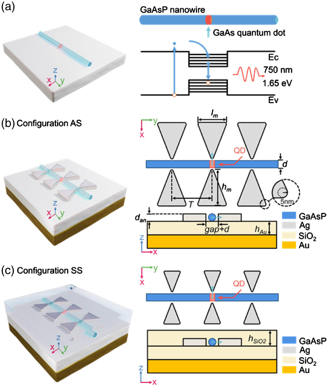
Figure 1.(a) Schematic of the NWQD (left); schematic energy band diagram for the QD embedded in a nanowire (right). (b) Configuration AS, NWQD coupled to a line-array plasmonic bowtie nanoantenna in an air superstrate with a gold mirror. (c) Configuration SS, NWQD coupled to a line-array plasmonic bowtie nanoantenna in a
From the fabrication perspective, GaAsP nanowires can be grown by a Ga-assisted VLS process, and a GaAs QDs region can be formed by switching off the phosphorus supply [3]. A PMMA-mediated transfer printing technique can manufacture the bowtie–NWQD structure [35]. The superstrate can be fabricated by standard coating, i.e., electron beam evaporation.
Numerical simulations are performed using finite element methods via COMSOL Multiphysics software to investigate the emission enhancement of the proposed structures, as shown in Fig. 9 (Appendix A). The QD is regarded as a two-level system, and thus, its emission can be modeled as an electric point dipole in the simulation [14,36]. The QD is assumed to have a high internal quantum yield [36]; the ohmic losses of the structure are determined by the non-radiative decay rate [37]. The detailed derivation process is shown in Appendix A. The SE enhancement of NWQD SPE can be evaluated by the Purcell factor and the fluorescence enhancement [38]:
Since a single NWQD will suppress the SE of QDs when the diameter is too small [39], to reflect the enhancement of the designed structure compared to NWQDs with the same diameter, we used the ratio to measure the enhancement ability of the structure to NWQDs, which is defined by Eq. (4):
3. RESULTS AND ANALYSIS
To understand the SE properties of a single NWQD, the emission of an uncoupled NWQD is first briefly investigated, as shown in Fig. 1(a). A cylindrical NWQD with diameter is placed horizontally on a silica substrate. We simulate the SE of NWQDs, considering it a point electric dipole placed at the center of the cylindrical nanowire. The radiation wavelength of the QD in a vacuum is 750 nm, and the dipole moment of the QD is perpendicular to the axis of the nanowire. The refractive index of GaAsP ( around ) is taken from Ref. [40].
Figure 2(a) shows the relationship between the of the GaAsP/GaAs NWQD and the diameter of the nanowire. Since the model does not involve a metal structure, no additional loss channel is introduced. According to Eqs. (1) and (2), and are the same, and will not be discussed for the time being. The of the GaAsP/GaAs NWQD varies with the diameter , as shown in Fig. 2(a). The of a single NWQD increases gradually with the diameter . It is consistent with the results in Refs. [39,41,42]. When is small, the nanowire diameter is too small to provide an efficient waveguide mode for the emitter. The coupling of the fundamental waveguide mode disappears rapidly, resulting in suppressed QD radiation [32]. As a result, is very low (). The calculated radiation suppression is in good agreement with experimental studies [43]. The cylindrical waveguide has relatively poor control of the beam propagation. The far-field pattern for a small-diameter () NWQD in free space appears as a doughnut shape the same as that of the electric point dipole, as shown in Fig. 2(d). The beam will be directed to both sides after placing the NWQDs on the substrate due to the sudden refractive index change at the interface, as shown in Figs. 2(b) and 2(c). When the NWQD diameter is increased to 140 nm, the mode appears. The increases to around 1, and most of the radiation is directed to both ends of the NWQD, showing good optical field confinement and directivity, as shown in Figs. 2(e)–2(g). In conclusion, for the NWQD with a large diameter, the value of can exceed 1 due to the emergence of waveguide modes, while for the NWQD with a small diameter, the SE is greatly suppressed. Next, we will try to enhance the SE of the NWQD with a small diameter, which is already suppressed by using plasmonic antennas, thus improving the structure’s directivity.
![]()
Figure 2.(a) Trend of the variation of
Further, we investigated the effect of the NWQD–single bowtie antenna-coupled devices. As shown in Fig. 3(a), a single bowtie antenna aligned with the center of the NWQD was placed horizontally on the substrate. The size of the bowtie has been optimized to ensure the best coupling effect at the wavelength of 750 nm. The relationship diagram of the size of the bowtie with respect to and is shown in Fig. 3(b). When , , and , the simulation results show that the and of the structure reach 52.3 and 47.1, respectively, and the ohmic loss is minimal, only 10% of the total radiated power. The SE direction of the device is divergent. The SE rate is enhanced by a factor of 1040 compared to a single NWQD of the same diameter (without plasmonic antenna coupling). Figure 3(c) shows the far-field pattern of a single bowtie–NWQD coupling structure, with the main lobe shifted downward due to the influence of the substrate. In contrast, the far-field pattern of a single bowtie antenna–NWQD coupling structure in free space is shown in Fig. 3(d). Comparing Fig. 2(d) and Fig. 3(d), it can be seen that the bowtie antenna has little effect on the spontaneous radiation direction of the NWQD. Its far-field pattern is similar to that of a point electric dipole.
![]()
Figure 3.(a) The NWQD coupled to a single plasmonic bowtie nanoantenna. (b)
We also simulated the effect of the relative distance between the plasmonic antenna and the QD on the enhancement effect, as shown in Fig. 10 (Appendix B). Like most reported plasmonic–quantum dot coupling structures, the relative distances of the plasmonics and QDs are directly related to the effect of the coupling [31]. The near-field enhancement of the plasmonic is only effective in the near field. When the distance is greater than 40 nm, the coupling between the QD and the plasmonic becomes weak, and the corresponding and are almost zero, as shown in Fig. 10.
After this, we periodically arrange three bowtie antennas into a line array and combine them on the NWQD, as shown in Fig. 4(a). , , and . The relationship between the SE performance of the structure and the period is shown in Fig. 4(b). When , the SE performance of the line-array bowtie antenna–NWQD coupling structure is optimized, the of the coupling structure reaches a maximum of 60.4, and the is 52.8. The spontaneous radiation phases of the three bowtie antennas are superimposed on each other, forming a wavefront parallel to the plane of the substrate, as shown in Figs. 4(c) and 4(d). Three hot spots appear at the tips of the three pairs of plasmonic antennas and coherently superimpose locally to form a plane-like wavefront. Correspondingly, the far-field radiation pattern of the whole structure exhibits directional emission in the vertical direction. Two downward sidelobes appear due to the sudden change of refractive index at the substrate, as shown in Fig. 4(e). Additional plasmonic antennas on both sides optimize the directivity of the device. Interestingly, compared with the NWQD coupled to a single plasmonic bowtie nanoantenna, the SE pattern of the NWQD coupled to a line-array plasmonic bowtie nanoantenna is more concentrated, and the and are increased by , as shown in Figs. 3(e) and 4(e). In other words, the additional plasmonic antennas on both sides enhance the directivity of the structural SE and its spontaneous emission rate. It is an enhancement mechanism that is completely different from Fig. 10. The QD is located in the center of the whole device [red area in Fig. 4(a)], while the distance between the plasmonic antennas on both sides is 420 nm from the QD, far exceeding the plasma coupling distance in Fig. 10. To explore the mechanism of this over-distance enhancement, we calculated the electric field distributions of a single plasmonic antenna and three pairs of the plasmonic antennas under plane wave excitation, as shown in Fig. 5(a). At the center of the middle plasmonic antenna, the near-field electric field modes of the single plasmonic antenna and the three-segment plasmonic antenna excited by the plane wave are and , respectively. It can be seen that the plasmonic antennas on both sides are far away from the QD and do not couple directly with the emission from the QD. However, the line-array structure composed of three pairs of plasmonic antennas can enhance the near-field strength of the central plasmonic antenna, thereby increasing the DOS near the QD. This far-field enhancement mechanism can increase the SE rate of a device beyond the plasmon decay length of the metal–dielectric interface.
![]()
Figure 4.(a) The NWQD coupled to a line-array plasmonic bowtie nanoantenna. (b)
![]()
Figure 5.(a) Electric field mode distributions of three pairs and a single plasmonic antenna under plane wave excitation. (b) Schematic diagram of single QD–line-array plasmonic antennas-coupled device. (c) Electric field mode distribution (V/m) and far-field radiation pattern (V/m) of single QD–line-array plasmonic antennas-coupled device, and the three red dots represent the tips of the three bowties.
As shown in Fig. 11 (Appendix C), we also calculated the spontaneous radiation effect of five pairs of plasmonic antennas. The outermost antenna negatively influences the whole structure because it is too far from the QD (). The hot spots generated by the antenna excitation cannot be observed in the electric field distribution diagram of the device, and the and of the five pairs of antenna coupling structures are 59.2 and 51.7, respectively. Therefore, the optimal number of line-array plasmonic antennas is determined to be three pairs.
The nanowires also play a crucial role in the device, and we simulated a single QD–line-array plasmonic antennas-coupled device without nanowires, as shown in Figs. 5(b)–5(d). In the absence of nanowires, it is difficult to observe the hot spots of the plasmonic antennas on both sides. Correspondingly, the device has poor directivity with large sidelobes on both sides. The nanowire ensures only one QD in a device and acts as a bridge here, passing the QD’s electromagnetic waves to the plasmonic antennas on either side. Because of the nanowire, the plasmonic antennas on both sides can collect the emission from the QDs within the waveguide and enhance the surface-emitting efficiency via the line-array antenna.
The effectiveness of the proposed design of the line-array antenna can be examined by simplifying the model to calculate the spontaneous radiation results of the whole structure theoretically. Comparing Fig. 2(d) and Fig. 3(d), it can be found that the SE of a single bowtie antenna-coupled NWQD is very similar to that of a single-point electric dipole. Therefore, the whole model can be simplified to a line-array model of three-point electric dipoles, as shown in Fig. 6(a). According to the phase distribution shown in Fig. 4(d), the phases of the bowtie on both sides lag behind the central bowtie. The spontaneous emission of the NWQD first excites the bowtie in the middle. After the propagation of (in nm), the electromagnetic wave reaches the bowtie on both sides and excites the sidelobes of the antenna. Therefore, the bowtie antenna on both sides has a phase difference , compared to the bowtie antenna at the center. The simplified model assumes that all three-point electric dipoles have magnitudes . The radiation field distribution of a point electric dipole is given by [44]
![]()
Figure 6.(a) Schematic diagram of a simplified mathematical model of the line-array antenna. (b) Main lobe directivity of the far-field radiation pattern of the simplified mathematical model of the line-array antenna. The inset is far-field patterns for different
The total field is given by
The transformation formulas of unit vectors of different coordinate systems contained therein are described in Eqs. (F1)–(F5). By bringing Eqs. (5)–(7) and Eqs. (F1)–(F5) into Eq. (8), the total far-field pattern of the whole model can be quantitatively calculated. Figure 6(b) depicts the far-field pattern directivity versus period for the proposed simplified line-array point-point dipole model. As increases, the directionality of the simplified model first increases and then decreases. When is small, the far-field pattern of the simplified model is similar to that of a single-point electric dipole. When reaches about 480 nm, the far-field pattern of the established simplified model shows vertical emission, and the directivity reaches a maximum of about 8.9 dB. If continues to increase, the far-field pattern of the established simplified model will have two sidelobes in the horizontal direction, and the vertical orientation will deteriorate. The radiation performance of the simplified model is similar to the spontaneous emission performance of the coupling structure of the three-section bowtie plasmonic line-array antenna–NWQD. The directional emission occurs at about 420 nm, proving that the proposed line-array bowtie antenna structure works. In the simplified model, we assume that the amplitudes of the three-point electric dipoles are the same. However, in the real case, the excitation of the bowtie on both sides will be smaller than that of the central bowtie antenna, so the optimal of the two models deviates. Due to the abrupt change in the boundary refractive index caused by the substrate, the far-field pattern of the coupling structure of the three-section bowtie wire array antenna–NWQD has two small sidelobes.
We have theoretically demonstrated that the vertical directional emission of our proposed line-array bowtie antenna–NWQD coupling structure benefits from the line-array structure. Next, we will further optimize the performance of the entire SPE.
To realize the vertical upward spontaneous emission of the SPE, we design a mirror resonator at the bottom of the structure and construct the AS, as shown in Fig. 1(b). The gold mirror is placed at a specific distance below the SPE. The electromagnetic waves radiated downward by the SPE are reflected upward and coherently superimposed to the radiation above as in an cavity. Figure 7(a) depicts the , , and ratios of the AS as a function of . After optimization, the final dimensions of the AS are , , diameter of NWQD , and . The of the AS reaches 66.1, the is 52.7, and the loss fraction is only 20.2%. Compared with a single NWQD of the same diameter (without plasmonic antenna coupling), the fluorescence of the AS is enhanced by 1054 times ( ratio = 1054). Meanwhile, the AS shows good directional radiation performance. Figures 7(b) and 7(c) depict the instantaneous electric field profile and far-field pattern of the AS, respectively. Three hot spots can be seen in the electric field distribution diagram, corresponding to three bowtie antennas. The spontaneous radiation of the three antennas is superimposed on each other to form parallel wavefronts. The far-field pattern of the AS has only one main lobe, and the directivity reaches 16 dB. We also analyzed the effect of the relative errors of the NWQD and plasmonic antenna positions in the AS on the spontaneous emission rate of the device, as shown in Fig. 12 (Appendix D).
![]()
Figure 7.(a)
Due to the different refractive indices of the substrate and air, two sidelobes appear in the downward radiation of the structure, as shown in Fig. 4(e), which will undoubtedly degrade the performance of the SPE. The SS with an additional coating can improve this phenomenon, as shown in Fig. 8. At the same time, due to the increase of the refractive index around the NWQD, the LDOS around the structure is improved, which further increases the SE rate of the constructed SPE. Figures 16 and 17 (Appendix E) show the effect of coating thickness on device performance.
![]()
Figure 8.(a)
![]()
Figure 9.Schematic diagram of the structure used in the physics simulation. Perfectly matched layers are placed outside the physical domain to simulate the propagation of electromagnetic waves in free space (absorbing electromagnetic waves to prevent reflected waves from affecting the structure itself).
![]()
Figure 10.Influence of relative distance between the plasmonic antenna and the QD on enhancement effect.
![]()
Figure 11.Distribution of electric field film (V/m) of five-pair plasmon antenna–NWQD coupling structure. Five-pair plasmon antenna–NWQD coupling structure electric field film distribution. The red outline is the NWQD, and the five red dots represent the tips of the three bowties.
![]()
Figure 12.Effect of the relative errors of the NWQD and plasmonic antenna positions in the AS.
As shown in Fig. 8(a), we investigate the , , and the ratio of the SS with different . After optimization, the final dimensions of the SS are , , , , and . The simulation results show that the of the SS reaches 185.6, the is 145.8, and the loss fraction is as small as 21%. Compared to a single NWQD of the same diameter (without plasmonic antenna coupling), the fluorescence of the SS is enhanced by a factor of 2916 ( ratio = 2916). Figure 8(c) shows the directional radiation pattern for the SS. The emitted photons are effectively directed toward the direction, and the directivity reaches 13 dB. Figure 13 (Appendix D) shows the effect of relative errors of NWQD and plasmonic antenna positions in the SS on device performance.
![]()
Figure 13.Effect of the relative errors of the NWQD and plasmonic antenna positions in the SS.
![]()
Figure 14.Collection efficiency of the SS with a different numerical aperture (NA).
![]()
Figure 15.Collection efficiency of the AS with a different numerical aperture (NA).
4. CONCLUSIONS
In our designs, the configuration of the linear array antenna is used to realize high-quality directional generation in a compact size, which abandons the traditional optical structure characterized by much larger size. The plasmonic antennas on both sides improve the directivity of the device through coherent superposition of beams while enhancing the SE rate of QDs through an over-range enhancement mechanism, in which the nanowires act as bridges. The two proposed structures exhibit good performance effects in terms of SE; compared with NWQDs of the same diameter, the two proposed structures achieve 1054 and 2916 times fluorescence enhancement, respectively. In addition, the proposed structures have lower non-radiative ohmic losses, which is maintained at around 20%, in comparison with the metal nanowire [46], metal-clad structures [47,48], metal gap structure [49], and Bragg grating [15–17,45], which were demonstrated to have a large non-radiation ohmic loss. It is worth noting that the small-diameter NWQD itself will suppress its SE rate, while the nanoantenna overcompensates the SE of the small nanowire. This can result in a lower and intensity. However, compared with the NWQD of the same diameter, the enhancement factor of our devices is impressively higher. Notably, the coupling of the NWQDs and the plasmonic antenna can guarantee that there is only one QD in the device. The three bowties are excited by only one QD, which guarantees the coherence of the bowtie radiation. The directional enhancement of the SPE is further achieved by the superposition coherence of the line array.
In conclusion, we propose two structures to enhance the SE of NWQDs via a line-array plasmonic antenna. Numerical simulations show that the of the two structures reaches 66.1 and 185.6, and the reaches 52.7 and 145.8, respectively. The fluorescence is 1054 and 2916 times higher than that of a single NWQD of the same diameter (without plasmonic antenna coupling). The plasmonic bowtie structure can significantly boost the SE of the NWQD with a small diameter in which the SE is seriously suppressed. Also, it has good directional radiation. The theoretical collection efficiencies reached 85% (NA = 0.5) and 80% (NA = 0.5), respectively. Under the premise of ensuring low ohmic loss, high , and small size, directional emission comparable to the coupling of traditional optical devices is achieved. The proposed SPE design is an alternative architecture at the nano/micro scale compared to conventional optics and has potential applications in future miniaturization and on-chip integration. It is worth mentioning that this method of enhancing single quantum dots with multiple structures has great research potential. Since the enhancement of quantum dots by plasmons is limited to the near-field region, conventional devices’ enhancement of quantum dots can often not be superimposed multiple times. Using our proposed new mechanism, we are expected to simultaneously achieve multiple plasmonic enhancements of a single QD. We anticipate that the design demonstrated in this work will facilitate SPE development and potentially integrate with semiconductor optoelectronics.
APPENDIX A: SIMULATION SETTING METHOD
In the simulation of quantum dots, quantum dots are generally regarded as a two-level system, which is set as a point current element [
The enhancement of the total decay rate is expressed by the Purcell factor, . The enhanced fluorescence of the device can be obtained when the non-radiative decay rate is neglected in . Since the ratio of the decay rate is proportional to the radiated power ratio, , , and can be expressed as
As the quantum dot is considered ideal and isolated from any neighboring dots or quantum confined structures, the non-radiative recombination is considered negligible. It is generally assumed that the intrinsic quantum yield of quantum dots is very high [
Numerical simulations are performed using finite element methods via COMSOL Multiphysics software to investigate the emission enhancement of the proposed structures, as shown in Fig.
APPENDIX B: EFFECT OF RELATIVE DISTANCE BETWEEN PLASMONIC ANTENNA AND QD ON COUPLING STRENGTH
The effect of the relative distance between the plasmonic antenna and the QD on the SE of the device is explored, as shown in Fig.
APPENDIX C: SPONTANEOUS RADIATION OF FIVE PAIRS OF PLASMONIC ANTENNAS
The electric field mode distributions of the five pairs of plasmonic antenna–QD coupling device are shown in Fig.
APPENDIX D: THE AS AND SS DEVICES RELATIVE ERROR AND COLLECTION EFFICIENCY
Considering the experimental error, we also analyzed the offset effect between the QD and the gap center of the bowtie. As shown in Figs.
The collection efficiencies of the AS and SS are calculated as shown in Figs.
APPENDIX E: THE EFFECT OF hSiO2 IN SS ON DEVICE PERFORMANCE
The performance effect of on the SS without a gold mirror is shown in Fig.
![]()
Figure 16.Performance effect of
![]()
Figure 17.Far-field radiation pattern of the SS without gold mirrors with different
APPENDIX F: COORDINATE CONVERSION FORMULA
The conversion formula between the three coordinate systems is
References
[1] R. H. Hadfield. Single-photon detectors for optical quantum information applications. Nat. Photonics, 3, 696-705(2009).
[2] I. Aharonovich, D. Englund, M. Toth. Solid-state single-photon emitters. Nat. Photonics, 10, 631-641(2016).
[3] P. Yu, Z. Li, T. Wu, Y.-T. Wang, X. Tong, C.-F. Li, Z. Wang, S.-H. Wei, Y. Zhang, H. Liu, L. Fu, Y. Zhang, J. Wu, H. H. Tan, C. Jagadish, Z. M. Wang. Nanowire quantum dot surface engineering for high temperature single photon emission. ACS Nano, 13, 13492-13500(2019).
[4] C. Wu, S. Kumar, Y. Kan, D. Komisar, Z. Wang, S. I. Bozhevolnyi, F. Ding. Room-temperature on-chip orbital angular momentum single-photon sources. Sci. Adv., 8, eabk3075(2021).
[5] F. Ripka, H. Kübler, R. Löw, T. Pfau. A room-temperature single-photon source based on strongly interacting Rydberg atoms. Science, 362, 446-449(2018).
[6] N. Mizuochi, T. Makino, H. Kato, D. Takeuchi, M. Ogura, H. Okushi, M. Nothaft, P. Neumann, A. Gali, F. Jelezko, J. Wrachtrup, S. Yamasaki. Electrically driven single-photon source at room temperature in diamond. Nat. Photonics, 6, 299-303(2012).
[7] X. He, H. Htoon, S. K. Doorn, W. H. P. Pernice, F. Pyatkov, R. Krupke, A. Jeantet, Y. Chassagneux, C. Voisin. Carbon nanotubes as emerging quantum-light sources. Nat. Mater., 17, 663-670(2018).
[8] M. Toth, I. Aharonovich. Single photon sources in atomically thin materials. Annu. Rev. Phys. Chem., 70, 123-142(2019).
[9] C. Santori, D. Fattal, J. Vučković, G. S. Solomon, Y. Yamamoto. Indistinguishable photons from a single-photon device. Nature, 419, 594-597(2002).
[10] S. Unsleber, D. P. S. McCutcheon, M. Dambach, M. Lermer, N. Gregersen, S. Höfling, J. Mørk, C. Schneider, M. Kamp. Two-photon interference from a quantum dot microcavity: persistent pure dephasing and suppression of time jitter. Phys. Rev. B, 91, 075413(2015).
[11] T. Grange, N. Somaschi, C. Antón, L. De Santis, G. Coppola, V. Giesz, A. Lemaître, I. Sagnes, A. Auffèves, P. Senellart. Reducing phonon-induced decoherence in solid-state single-photon sources with cavity quantum electrodynamics. Phys. Rev. Lett., 118, 253602(2017).
[12] T. B. Hoang, G. M. Akselrod, M. H. Mikkelsen. Ultrafast room-temperature single photon emission from quantum dots coupled to plasmonic nanocavities. Nano Lett., 16, 270-275(2016).
[13] A. R. Dhawan, C. Belacel, J. U. Esparza-Villa, M. Nasilowski, Z. Wang, C. Schwob, J.-P. Hugonin, L. Coolen, B. Dubertret, P. Senellart, A. Maître. Extreme multiexciton emission from deterministically assembled single-emitter subwavelength plasmonic patch antennas. Light Sci. Appl., 9, 33(2020).
[14] T. B. Hoang, G. M. Akselrod, C. Argyropoulos, J. Huang, D. R. Smith, M. H. Mikkelsen. Ultrafast spontaneous emission source using plasmonic nanoantennas. Nat. Commun., 6, 7788(2015).
[15] M. Moczała-Dusanowska, Ł. Dusanowski, S. Gerhardt, Y. M. He, M. Reindl, A. Rastelli, R. Trotta, N. Gregersen, S. Höfling, C. Schneider. Strain-tunable single-photon source based on a quantum dot–micropillar system. ACS Photonics, 6, 2025-2031(2019).
[16] G. Yang, Q. Shen, Y. Niu, H. Wei, B. Bai, M. H. Mikkelsen, H. B. Sun. Unidirectional, ultrafast, and bright spontaneous emission source enabled by a hybrid plasmonic nanoantenna. Laser Photonics Rev., 14, 1900213(2020).
[17] H. Abudayyeh, B. Lubotzky, A. Blake, J. Wang, S. Majumder, Z. Hu, Y. Kim, H. Htoon, R. Bose, A. V. Malko, J. A. Hollingsworth, R. Rapaport. Single photon sources with near unity collection efficiencies by deterministic placement of quantum dots in nanoantennas. APL Photonics, 6, 036109(2021).
[18] F. Huang, M. Li, F. Chen, H. Zhang, Q. Li. Gap surface plasmon and plasmonic waveguide based single photon source. 17th International Conference on Numerical Simulation of Optoelectronic Devices (NUSOD), 43-44(2017).
[19] H. Hao, J. Ren, X. Duan, G. Lu, I. C. Khoo, Q. Gong, Y. Gu. High-contrast switching and high-efficiency extracting for spontaneous emission based on tunable gap surface plasmon. Sci. Rep., 8, 11244(2018).
[20] S. Hepp, F. Hornung, S. Bauer, E. Hesselmeier, X. Yuan, M. Jetter, S. L. Portalupi, A. Rastelli, P. Michler. Purcell-enhanced single-photon emission from a strain-tunable quantum dot in a cavity-waveguide device. Appl. Phys. Lett., 117, 254002(2020).
[21] X. Huang, X. Tong, Z. Wang. Rational design of colloidal core/shell quantum dots for optoelectronic applications. J. Electron. Sci. Technol., 18, 100018(2020).
[22] V. Krivenkov, P. Samokhvalov, I. Nabiev, Y. P. Rakovich. Synergy of excitation enhancement and the Purcell effect for strong photoluminescence enhancement in a thin-film hybrid structure based on quantum dots and plasmon nanoparticles. J. Phys. Chem. Lett., 11, 8018-8025(2020).
[23] K. Santhosh, O. Bitton, L. Chuntonov, G. Haran. Vacuum Rabi splitting in a plasmonic cavity at the single quantum emitter limit. Nat. Commun., 7, 11823(2016).
[24] A. Neogi, H. Morkoc, T. Kuroda, A. Tackeuchi, T. Kawazoe, M. Ohtsu. Exciton localization in vertically and laterally coupled GaN/AlN quantum dots. Nano Lett., 5, 213-217(2005).
[25] M. S. Skolnick, D. J. Mowbray. Self-assembled semiconductor quantum dots: fundamental physics and device applications. Annu. Rev. Mater. Res., 34, 181-218(2004).
[26] A. Neogi, B. Gorman, H. Morkoç, T. Kawazoe, M. Ohtsu. Near-field optical spectroscopy and microscopy of self-assembled GaN/AlN nanostructures. Appl. Phys. Lett., 86, 043103(2005).
[27] P. Yu, J. Wu, L. Gao, H. Liu, Z. Wang. InGaAs and GaAs quantum dot solar cells grown by droplet epitaxy. Solar Energy Mater. Sol. Cells, 161, 377-381(2017).
[28] M. Pfeiffer, P. Atkinson, A. Rastelli, O. G. Schmidt, H. Giessen, M. Lippitz, K. Lindfors. Coupling a single solid-state quantum emitter to an array of resonant plasmonic antennas. Sci. Rep., 8, 3415(2018).
[29] J. Lee, A. O. Govorov, J. Dulka, N. A. Kotov. Bioconjugates of CdTe nanowires and Au nanoparticles: plasmon-exciton interactions, luminescence enhancement, and collective effects. Nano Lett., 4, 2323-2330(2004).
[30] J. Lee, P. Hernandez, J. Lee, A. O. Govorov, N. A. Kotov. Exciton-plasmon interactions in molecular spring assemblies of nanowires and wavelength-based protein detection. Nat. Mater., 6, 291-295(2007).
[31] B. Wang, P. Yu, W. Wang, X. Zhang, H.-C. Kuo, H. Xu, Z. M. Wang. High-
[32] G. Bulgarini, M. E. Reimer, T. Zehender, M. Hocevar, E. P. Bakkers, L. P. Kouwenhoven, V. Zwiller. Spontaneous emission control of single quantum dots in bottom-up nanowire waveguides. Appl. Phys. Lett., 100, 121106(2012).
[33] P. Li, P. Yu, W. Wang, F. Lin, H. Xu, Z. Wang. Efficient single-photon emission from a nanowire quantum dot coupled to a plasmonic nanoantenna. J. Lightwave Technol., 39, 7495-7501(2021).
[34] S. Kolatschek, C. Nawrath, S. Bauer, J. S. Huang, J. Fischer, R. Sittig, M. Jetter, S. L. Portalupi, P. Michler. Bright Purcell enhanced single-photon source in the telecom O-band based on a quantum dot in a circular Bragg grating. Nano Lett., 21, 7740-7745(2021).
[35] Z. Fang, L. Fan, C. Lin, D. Zhang, A. J. Meixner, X. Zhu. Plasmonic coupling of bow tie antennas with Ag nanowire. Nano Lett., 11, 1676-1680(2011).
[36] P. Anger, P. Bharadwaj, L. Novotny. Enhancement and quenching of single-molecule fluorescence. Phys. Rev. Lett., 96, 113002(2006).
[37] R. Chance, A. Prock, R. Silbey. Molecular fluorescence and energy transfer near interfaces. Adv. Chem. Phys., 37, 1-65(1978).
[38] P. Bharadwaj, L. Novotny. Spectral dependence of single molecule fluorescence enhancement. Opt. Express, 15, 14266-14274(2007).
[39] N. Mukhundhan, A. Ajay, J. Bissinger, J. J. Finley, G. Koblmüller. Purcell enhanced coupling of nanowire quantum emitters to silicon photonic waveguides. Opt. Express, 29, 43068-43081(2021).
[40] B. Conrad, A. Lochtefeld, A. Gerger, A. Barnett, I. Perez-Wurfl. Optical characterisation of III-V alloys grown on Si by spectroscopic ellipsometry. Solar Energy Mater. Sol. Cells, 162, 7-12(2017).
[41] I. Friedler, C. Sauvan, J. P. Hugonin, P. Lalanne, J. Claudon, J. M. Gérard. Solid-state single photon sources: the nanowire antenna. Opt. Express, 17, 2095-2110(2009).
[42] X. Guo, Y. B. Ying, L. M. Tong. Photonic nanowires: from subwavelength waveguides to optical sensors. Acc. Chem. Res., 47, 656-666(2014).
[43] J. Bleuse, J. Claudon, M. Creasey, N. S. Malik, J.-M. Gérard, I. Maksymov, J.-P. Hugonin, P. Lalanne. Inhibition, enhancement, and control of spontaneous emission in photonic nanowires. Phys. Rev. Lett., 106, 103601(2011).
[44] H. Matzner, M. Milgrom, S. Shtrikman. Magnetoelectric symmetry and electromagnetic radiation. Ferroelectrics, 161, 213-219(1994).
[45] M. Moczala-Dusanowska, L. Dusanowski, O. Iff, T. Huber, S. Kuhn, T. Czyszanowski, C. Schneider, S. Hoefling. Strain-tunable single-photon source based on a circular Bragg grating cavity with embedded quantum dots. ACS Photonics, 7, 3474-3480(2020).
[46] G. Zhang, S. Jia, Y. Gu, J. Chen. Brightening and guiding single-photon emission by plasmonic waveguide–slit structures on a metallic substrate. Laser Photonics Rev., 13, 1900025(2019).
[47] C. C. Chiang, S. I. Bogdanov, O. A. Makarova, X. Xu, S. Saha, D. Shah, Z. O. Martin, D. Wang, A. S. Lagutchev, A. V. Kildishev, A. Boltasseva, V. M. Shalaev. Chip-compatible quantum plasmonic launcher. Adv. Opt. Mater., 8, 2000889(2020).
[48] B. Ji, E. Giovanelli, B. Habert, P. Spinicelli, M. Nasilowski, X. Xu, N. Lequeux, J. P. Hugonin, F. Marquier, J. J. Greffet, B. Dubertret. Non-blinking quantum dot with a plasmonic nanoshell resonator. Nat. Nanotechnol., 10, 170-175(2015).
[49] W. Wei, X. Yan, J. Liu, B. Shen, W. Luo, X. Ma, X. Zhang. Enhancement of single-photon emission rate from InGaAs/GaAs quantum-dot/nanowire heterostructure by wire-groove nanocavity. Nanomaterials, 9, 671(2019).
[50] D. Magde, R. Wong, P. G. Seybold. Fluorescence quantum yields and their relation to lifetimes of rhodamine 6G and fluorescein in nine solvents: improved absolute standards for quantum yields. Photochem. Photobiol., 75, 327-334(2002).
[51] A. Kinkhabwala, Z. Yu, S. Fan, Y. Avlasevich, K. Müllen, W. E. Moerner. Large single-molecule fluorescence enhancements produced by a bowtie nanoantenna. Nat. Photonics, 3, 654-657(2009).
[52] M. Bauch, K. Toma, M. Toma, Q. Zhang, J. Dostalek. Plasmon-enhanced fluorescence biosensors: a review. Plasmonics, 9, 781-799(2014).
[53] J. McBride, J. Treadway, L. Feldman, S. J. Pennycook, S. J. Rosenthal. Structural basis for near unity quantum yield core/shell nanostructures. Nano Lett., 6, 1496-1501(2006).
[54] A. M. Smith, A. M. Mohs, S. Nie. Tuning the optical and electronic properties of colloidal nanocrystals by lattice strain. Nat. Nanotechnol., 4, 56-63(2009).
[55] T. Frecker, D. Bailey, X. Arzeta-Ferrer, J. McBride, S. J. Rosenthal. Review—quantum dots and their application in lighting, displays, and biology. ECS J. Solid State Sci. Technol., 5, R3019-R3031(2016).

Set citation alerts for the article
Please enter your email address
© Copyright 2018-2021 | Chinese Laser Press. All Rights Reserved 沪ICP备15018463号-20