
Yuan Yuan, Wayne V. Sorin, Di Liang, Stanley Cheung, Yiwei Peng, Mudit Jain, Zhihong Huang, Marco Fiorentino, Raymond G. Beausoleil. Mechanisms of enhanced sub-bandgap absorption in high-speed all-silicon avalanche photodiodes[J]. Photonics Research, 2023, 11(2): 337
- Photonics Research
- Vol. 11, Issue 2, 337 (2023)
Abstract
1. INTRODUCTION
Over the past two decades, Si photonics have become a promising technology that aims to reduce system-level power consumption to a few of subpicojoule/bit, increase aggregate bandwidth to multiple terabytes/second, and lower manufacturing costs by leveraging well-established CMOS technology. The high-refractive index contrast of the silicon-on-insulator (SOI) platform has enabled the foundation for large-scale photonic integrated circuits (PICs) and is widely regarded as a promising solution for next-generation optical communication [1,2], computing [3], sensing [4], etc. Bulk Si has a bandgap of and is therefore transparent at telecommunication wavelengths of 1310 and 1550 nm, thus making it superior for low-loss optical signal routing within dense and sophisticated PICs. Conversely, interband optical signal detection typically requires narrower bandgap materials to be integrated with the Si. The most common is germanium (Ge), which has a bandgap of corresponding to a cut-off wavelength up to . Numerous studies have been conducted to advance high-performance Si-Ge photodiodes (PDs) [5,6] and avalanche photodiodes (APDs) [7–11], which takes advantage of small impact ionization coefficient in Si over Ge and many other III-V compounds. Some foundries specializing in Si photonics, such as AMF, IMEC, GF, and AIM, have incorporated Ge deposition into their process design kits. However, low-temperature selective-area epitaxial growth of Ge on Si is required to achieve a high-quality Ge/Si interface. This increases fabrication cost and time and is not trivial or readily available in many other CMOS foundries, which may further impact system performance and reliability. Other materials such as III-V compounds [12,13] and related quantum wells [14,15], quantum dots [16–18], and 2D materials [19,20] have also been used as PDs on the Si photonics platform via heterogeneous/monolithic integration. Similarly, these devices require even more complicated hetero-epitaxy or heterogeneous integration processes, which are far less compatible with standard CMOS processing. These approaches, to this day, remain obstacles toward realizing reliable, low-cost, and volume-production-ready Si photonics.
Recently, all-Si PDs have drawn significant interest due to their “zero change” to traditional CMOS material and fabrication. Sub-bandgap absorption in Si, such as surface and bulk defect-mediated absorption, can detect wavelengths . Unfortunately, sub-bandgap absorption is too weak to achieve high responsivity. One way to enhance sub-bandgap absorption is to create deep-level defects in Si allowing midbandgap energy levels to assist electron excitation from the valence band to the conduction band. These defects/impurities require additional ions or implantation dopants [21–26]. Another method is to use surface-state absorption (SSA) between the interface [27]. Since SSA efficiency relies on the power overlap of the optical mode at the Si waveguide (WG) surface, responsivity is generally low. Another possibility is the internal photo-emission effect (IPE) where metal layers are deposited on the top of Si to form a Schottky barrier to absorb longer wavelengths [28]. However, IPE-based PDs are limited by high dark currents. Photon-assisted tunneling (PAT) is another method to absorb sub-bandgap wavelengths [29,30]. Under a high reverse electric field, the distance between the valence and conduction bands is shortened. Thus, electrons have an improved tunneling probability through the bandgap with the help of photons. Although the tunneling probability increases with higher electric field, the PD performance is ultimately limited by larger dark current. Another mechanism is two-photon absorption (2PA), which is a process where two photons are simultaneously absorbed. However, the third-order nonlinear coefficient of Si is small, thus limiting 2PA to applications using high optical intensities [31]. Several recent publications, including our internal work report good responsivity in Si microring resonators (MRRs) operating at telecommunication wavelengths such as 1310 nm without artificial defects [32–36]. However, it remains unclear whether the resonance-enhancement effort alone results in tremendous performance improvement under the condition of weak sub-bandgap absorption in Si [33].
In this paper, a high-performance all-Si MRR PD is studied as an example to explore the complex absorption mechanism. The MRR PD shares the same design as our recently demonstrated Si depletion-mode MRR modulator with the exception of different operating bias voltages. The Si MRR PD exhibits low operation voltage, high responsivity, and impressive high-speed performance with a key benefit of full CMOS compatibility, without the need for complex Ge processes. It allows the implementation of compact integrated optical transceivers and other PICs with virtually zero design change on conventional CMOS electronics process. This facilitates an ideal architecture for Ge-free wavelength division multiplexing (WDM) applications [37]. By measuring the responsivity of all-Si MRR PD at different bias voltages, wavelengths, and optical powers, the complex absorption mechanisms can be revealed. In particular, the avalanche gain significantly enhances the responsivity at a relatively high bias. For the first time, to the best of our knowledge, we introduce a model that fully describes the physics behind the high responsivity of the all-Si PD via the combination of four contributing mechanisms: photon-assisted tunneling (PAT); two photon absorption (2PA); resonance enhancement; and avalanche gain. While the MRR acts as the resonant cavity structure in this work, other traveling wave cavities or Fabry–Perot cavities apply to the same model.
Sign up for Photonics Research TOC. Get the latest issue of Photonics Research delivered right to you!Sign up now
2. RESULTS
A. Device Design
The schematic diagram of the all-Si MRR APD is shown in Fig. 1. We use a Si microring structure with two separate PN junctions whose length ratio is . The two-segment depletion-mode Si MRR structure was originally designed to realize pulse amplitude modulation with four levels (PAM4) more efficiently by biasing the long and short segments individually [38]. When reverse-biasing the device, the all-Si PN junction can also detect sub-bandgap wavelengths, e.g., 1310 nm. This device is studied thoroughly as an example to delineate the absorption mechanisms of the all-Si MRR APD. Compared to the reported MRR modulator with similar designs [38], this MRR APD has a larger quality factor () to result in better responsivity via resonance enhancement effect. In this work, we only probed the long segment PN junction for detection of light, and all data from the long segment junction are sufficient to develop a detailed model. For optimal PD design in the future, a single PN junction design, which is distributed throughout the MRR, is preferred for maximal light absorption volume and subsequently higher responsivity. The cross section of the Si microring WG is shown in the top left of Fig. 1. Both microring and bus WG share the same rib WG profile of 500 nm in width, 220 nm in height, and 90 nm in slab height. A racetrack configuration was adopted to realize power coupling between the microring and bus WG with a coupling gap of 180 nm. A simple lateral PN junction is formed within the WG core area of both short and long segments. Also, a TiN layer 2000 nm above the Si microring WG of straight coupling section is used as a heater to tune the resonance.
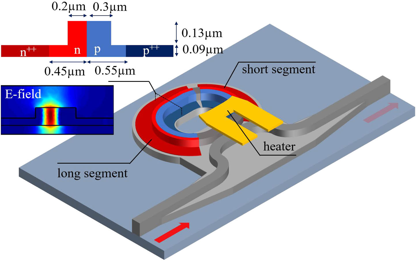
Figure 1.Schematic diagram of the Ge-free MRR APD.
B. DC Characterizations
The racetrack has a bend radius of and a straight section length of , which means that the equivalent radius of the MRR is , corresponding to a free spectral range (FSR) of near 1310 nm. At zero bias voltage, the measured normalized transmission spectrum is as shown in Fig. 2(a). It exhibits an FSR of as designed, a DC extinction ratio (ER) of , and a full width at half-maximum (FWHM), , of . From these values, intrinsic properties of the MRR can be extracted. The loaded quality factor can be calculated as , resulting in around 1310 nm. The finesse of the MRR is , which can also be expressed by
![]()
Figure 2.(a) Measured normalized transmission spectrum at zero bias voltage. (b) Schematic of an MRR device. (c) Simulated coupling coefficient with the 1310 nm TE mode light [38].
The Si PN junction-based MRR has been widely used as a depletion-mode modulator. The well-known plasma dispersion effect changes the refractive index when carrier density varies. Typically, a reverse DC voltage is added across the PN junction to keep it reverse-biased during AC modulation. However, things become different at a higher reverse bias: the PAT starts to become non-negligible and allows the Si PN junction to generate photocurrent from sub-bandgap wavelengths. The PAT probability can be written as [29,40]
![]()
Figure 3.Simulated (a) electric field and (b) energy band diagrams of the Si PN junction at different bias voltages.
To investigate the MRR PN junction at different operation conditions, 2D responsivity colormaps with respect to wavelength and reverse bias from 0 to at different optical injection power levels are plotted as shown in Fig. 4. The effects of three optical power levels, i.e., , 1.5, and 6.5 dBm, were examined, respectively. The optical power here refers to the power inside the input bus WG, i.e., . All responsivities refer to the ratio of photocurrent to the input bus waveguide optical power, with all enhancement mechanisms included. As shown in Fig. 4, the peak responsivity of the MRR APD always appears at resonance wavelength because of the maximal resonance enhancement inside the MRR. With the increase of reverse-bias voltage, the peak responsivity shifts to longer wavelengths and its maximum value rises as well. The resonance redshift is due to the reduction of carrier density at higher bias. It is noted that MRR resonance redshifts at a larger pace under higher optical input power. This is because more heat is generated inside the MRR to induce more resonance shift. Additionally, this heating effect causes the cavity resonance to exhibit thermal nonlinearities leading to an asymmetric triangular-shaped transmission spectrum.
![]()
Figure 4.Measured 2D colormaps of responsivity versus reverse-bias voltage and wavelength with bus WG power at (a)
Based on above 2D scan results, the response of the MRR APD at resonance wavelength can be extracted. Figure 5(a) shows both total and dark currents versus reverse bias; all total current points represent the maximal current values in each wavelength scan. Both total and dark currents increase with reverse bias, and the MRR APD generates a dark current of at . The wavelengths corresponding to the maximum total current points are defined as the resonance wavelength, which are shown in Fig. 5(b). Similarly, the resonance wavelength exhibits an exponential-like redshift because PAT absorption and avalanche gain increase exponentially at higher bias voltages. The corresponding responsivity at resonance wavelength is shown in Fig. 5(c). Since both PAT and avalanche effects become more significant with increased bias voltage, the responsivity increases as expected. One interesting effect is a higher responsivity for lower optical power. This phenomenon is similar to the power saturation of the avalanche gain in conventional APDs [41], which confirms the existence of avalanche gain. Overall, the MRR APD exhibits a peak responsivity up to at input power.
![]()
Figure 5.Measured (a) total and dark currents, (b) wavelength, and (c) responsivity at resonance with bus WG power at
C. MRR APD Absorption Model
There has been strong research interest in building efficient Ge-free Si PDs using different approaches [21–28]. The simplest implementation is the direct use of a Si PN junction via PAT. Although Eq. (3) shows that the PAT probability increases exponentially with narrower barrier width, it is difficult to generate a large useful photocurrent due to rapidly increased dark current simultaneously. On the other hand, the resonant optical gain in an MRR structure and avalanche effect can enhance this weak absorption mechanism. Here, we construct a model to systematically derive the contributing mechanisms for high responsivity in pure Si MRR photodetectors. As mentioned, the higher electric field leads to a narrower and thus a higher tunneling probability. In conjunction, the high electric field will also accelerate carriers and eventually cause impact ionization. Additionally, the MRR resonance enhancement effect builds stronger optical power inside the cavity, resulting in higher responsivity and subsequently more 2PA. Therefore, we have identified four main mechanisms to include in this model: PAT; 2PA; microring resonance enhancement effect; and avalanche gain. All symbols in the model are listed in Table 1. Symbol Meanings, Values, and Units for the MRR APD Absorption ModelSymbol Meaning Value Unit Responsivity \ A/W RE Resonance enhancement \ Avalanche gain \ \ One round-trip internal quantum efficiency \ \ Optical power in the input port bus WG \ mW Optical power in the ring WG \ mW Total cavity loss coefficient \ Coupling loss coefficient \ Ring propagation loss coefficient \ Gain fitting parameters 0.17, 4.56 \ Effective loss absorption coefficient Photocurrent generated absorption coefficient \ Optical mode confinement factor within the depletion region Two-photon absorption coefficient \ Two-photon absorption coefficient constant 0.9 cm/GW Total absorption coefficient \ Effective PN junction length cm Effective ring WG cross section area
The photocurrent of the MRR APD is expressed as
Based on the MRR APD absorption model, the photocurrent and responsivity versus under different bias voltages can be plotted and compared with the measurement results in Fig. 6. When the electric field is relatively small under a bias of , the probability of impact ionization can be ignored. However, unlike the conventional P-I-N PDs, the measured photocurrent is a slightly positive quadratic function of the optical power [Fig. 6(a)]. Since two photons are absorbed simultaneously in the 2PA process, the absorbed power is proportional to the square of the photon numbers, which gives the photocurrent a positive quadratic term of optical power. This indicates that a 2PA mechanism exists in the MRR APD. The responsivity at is shown in Fig. 6(b), which increases linearly with the optical power due to the 2PA. The photocurrent and responsivity trends at are quite different. Although 2PA still exists, the avalanche gain plays a dominant role. The optical power dependent gain can be expressed by Eq. (6). Consequently, the photocurrent in Fig. 6(c) shows a saturation trend with the increased optical power. Owing to the gain saturation, the responsivity of the MRR APD, shown in Fig. 6(d), decreases from under minimal optical input to under optical input at .
![]()
Figure 6.Measured and fitted photocurrent and responsivity versus bus WG power at reverse bias of (a), (b)
Substituting Eqs. (5)–(8) into Eq. (4), the photocurrent and responsivity of the MRR APD can be calculated. The parameters used in the model are listed in Table 1. As mentioned in Section 2.B, the , , and can be extracted from the MRR transmission spectrum. The loss absorption coefficient, , can be estimated from the FCA. The microring RE can then be calculated by these known loss values. The 2PA coefficient constant, , can be extracted from the measured photocurrent at , which is and is close to the reported of Si [31,42,43]. The effective absorption coefficient of PAT, , can be estimated from Eq. (3) and Fig. 3. The gain value under low optical input power is estimated from simulation. Figure 7(a) shows the simulated gain curve of the Si PN junction by using Lumerical Charge with low photon-generated carrier density, where the Si effective ionization coefficients were used due to the dead-space effect of the thin depletion region [44,45]. The Si PN junction can achieve a simulated avalanche gain of at . Based on Eq. (6), the calculated gain from 0.08 to 5.0 mW at is as shown in Fig. 7(b). This optical power dependent gain is also plotted in Fig. 7(a) at , i.e., the red line, which intersects the simulated gain at 0.1 mW. By using the listed values, the calculated photocurrent and responsivity are as shown as the black lines in Fig. 6, exhibiting excellent agreement with the measured data. Overall, the intrinsic photocurrent from a combination of PAT () and 2PA ( to 0.02%) only contributes absorption for one round-trip inside the microring. However, the resonance enhancement effect () and the avalanche gain () boost the weak absorption to enable a high total responsivity up to .
![]()
Figure 7.(a) Simulated avalanche gain versus bias voltage at 0.1 mW. (b) Fitted avalanche gain versus optical power at
D. RF Characterizations
Figure 8(a) shows the measured S11 response at bias voltages of , , and , where the solid and dash lines are the real and imaginary parts, respectively. Obviously, S11 is different at , especially at 0 GHz, where the real part of S11 becomes substantially less than 1. This indicates that the avalanche-induced dark current is reducing the device impedance, which is consistent with the measured dark current shown in Fig. 5(a). In the Smith chart of Fig. 8(b), the measured S11 at (red line) agrees well with the fitted S11 from the equivalent circuit (blue line). The equivalent circuit is illustrated in Fig. 8(c), where , , and are the junction capacitance, shunt resistance, and series resistance of the Si PN junction; is the current source that represents the generated photocurrent; , , are the parasitic parameters; and is the load resistance. The S11 was fitted with theoretically calculated and values, which ensures the rationality of fitting to the equivalent circuit. The RC time-limited 3 dB bandwidth can then be simulated based on it. Figure 8(d) illustrates the frequency response of the equivalent circuit; thus, a 3 dB bandwidth of can be obtained. Thanks to the small PN junction capacitance at the high electric field, the RC time will not limit the speed of the MRR APD.
![]()
Figure 8.(a) Measured S11 response of the MRR APD at bias voltage of
The small-signal opto-electric (O-E) response of the MRR APD at bias voltages of , , and is shown in Fig. 9(a). At each bias voltage, the S21 response was measured at the resonance wavelength (i.e., the wavelength with the highest responsivity after accounting for thermal-wavelength drifting). The 3 dB O-E bandwidth of the MRR APD shows a slight increase with higher reverse bias, from at to at . This is due to the higher PAT absorption efficiency at higher bias voltage and the increased absorption loss leading to a larger photon lifetime-limited bandwidth. Similar to other PDs, there is a trade-off between the bandwidth and the responsivity for MRR PDs. A higher factor improves the resonance enhancement for higher responsivity, while reducing the photon lifetime-limited bandwidth [46]. High-speed nonreturn-to-zero (NRZ) and PAM4 eye diagrams were demonstrated with pseudo random bit sequence 9 (PRBS9) signals. There is no amplifier after the MRR APD; thus, high optical power is needed to provide detectable electric signals in the oscilloscope, which is 6.5 dBm inside the bus WG. The measured 80 Gb/s NRZ and 100 Gb/s PAM4 eye diagrams at are shown in Figs. 9(b) and 9(c), respectively. Even though the MRR APD exhibits a 3 dB bandwidth of at , the roll-off of its O-E response is not too steep. This is due to the RC-limited bandwidth () being higher than 50 GHz; thus, the poles of the RC do not yet affect the roll-off slope. Its 10 dB bandwidth corresponds to ; as such, it can support open-eye diagrams up to 100 Gb/s.
![]()
Figure 9.(a) Measured O-E S21 response at resonance. Measured eye diagrams of (b) 80 Gb/s NRZ and (c) 100 Gb/s PAM4 modulations with 6.5 dBm optical power in the bus WG at bias voltage of
The amplitude of the eye diagrams suffers from equipment limitations. The MRR APD has to work at , which relates to a low responsivity of . By adding a trans-impedance amplifier, the MRR APD yields eye diagrams at lower optical power, which will allow responsivity up to . Moreover, as described in the device design section, it is a two-segment device for modulator design. For an optimized Ge-free MRR APD, a single long PN junction is more suitable than the current two-segment design. It will bring at least 50% more responsivity for such an MRR APD, which means the responsivity can reach up to .
3. DISCUSSION
A. Absorption in Straight Waveguide
More broadly, the all-Si straight waveguide based on a PN junction can also be used as a photodetector. Due to the lack of a microring cavity, the resonance enhancement effect is not needed in the model. Further, the two-photon absorption (2PA) can be neglected because of the relatively low intensity of light without resonance enhancement. Therefore, the model is simplified as
![]()
Figure 10.Calculated responsivity of the all-Si straight waveguide with 1 mW input optical power at
B. Conclusion
In this work, we established a comprehensive sub-bandgap absorption model for all-Si PDs and validated this model with a Ge-free all-Si MRR APD at O-band wavelengths. The example MRR APD exhibits a total responsivity of , a 3 dB bandwidth of , a dark current of , and open-eye diagrams of 80 Gb/s NRZ and 100 Gb/s PAM4 at . Four mechanisms, PAT, 2PA, resonance enhancement, and avalanche gain jointly contribute to the high responsivity of the all-Si APD.
The relatively low working voltage can reduce power consumption and is more compatible with architectures using limited voltage supplies. Compared with other O-band PDs, the MRR APD only uses Si to form the PN junction, thus requiring no additional processes such as monolithic epitaxy, heterogeneous integration, and defect assisted implantation. As a fundamental building block in Si photonics, the Si-based PN junction undoubtedly simplifies foundry process complexity of implementing PDs. This results in shorter research and product development cycles with an added cost benefit. Moreover, the inherent resonance of the MRR APD makes it suitable for WDM applications. As a combination of a wavelength demultiplexer (DMUX) and PD, the MRR APD also enables a smaller footprint for a WDM Rx [47]. Since the avalanche gain is higher for relatively weak signals, this all-Si APD is particularly suitable for WDM links with limited optical power. One example is comb laser-based dense WDM (DWDM) links; peak wavelength power for each comb is typically weaker compared with DFB laser arrays [48]. Hence, an all-Si MRR APD array could be an ideal DMUX for detecting high-speed, weak optical signals.
According to theoretical and experimental studies, we found PAT and 2PA mechanisms exist and simultaneously contribute to the absorption of at . This absorption is then improved via MRR resonance enhancement and APD avalanche gain, which both amplify the photocurrent to generate the final total responsivity. The developed model unfolds the contributing mechanisms of all-Si MRR APDs, which offer a way to improve the device performance. The responsivity of the all-Si MRR APD can be further enhanced by the following: (1) reducing MRR propagation loss, which does not generate photocurrent (smaller ); (2) achieving MRR critical coupling (larger RE); (3) increasing the optical mode overlap with the Si depletion region (larger ); and (4) increasing the electric field within the depletion region (larger and ).
4. MATERIALS AND METHODS
A. Fabrication
The MRR APD chips were fabricated by joining a multiproject-wafer (MPW) run at Advanced Micro Foundry (AMF), Singapore. The chips are based on industry standard 220 nm thick silicon-on-insulator (SOI) wafers with all Si doping levels fixed by the foundry design rule. The doping levels were simulated based on the foundry-provided sheet resistances, where the - and -type doping is , and and doping is .
B. S-parameters Measurements
The S-parameters of the MRR APD were measured with a 50 GHz vector network analyzer (VNA). S11 was measured after cable and probe calibration. For S21, a 65 GHz Mach–Zehnder modulator (MZM) was used to modulate the optical signals with the electrical signals from the VNA; after that, the MRR APD-generated electrical signals were captured by the VNA. The frequency response of all other components, such as MZM, bias-tee, and RF cables, has been calibrated.
C. Eye Diagram Measurements
The eye diagrams of the MRR APD have been measured with a 92 GSa/s arbitrary waveform generator (AWG), which provided PRBS9 signals for the MZM. Thus, the 65 GHz MZM can modulate light from a tunable O-band laser. After that, a praseodymium-doped fiber amplifier (PDFA) was used to compensate the MZM insertion loss, fiber loss, and grating coupler loss. The amplified light was injected into the all-Si MRR APD; then, the detected electric signals were captured by a 60 GHz digital communication analyzer oscilloscope (DCA) via a 45 GHz bias-tee. All signal distortions caused by the MZM, bias-tee, and RF cables are calibrated by the AWG internal calibration function. Due to the setup limitation, there is no wideband O-band optical filter to reduce the PDFA amplified spontaneous emission (ASE) noise; hence, all eye diagrams were averaged by 32 times.
References
[10] B. Shi, F. Qi, P. Cai, X. Chen, Z. He, Y. Duan, G. Hou, T. Su, S. Li, W. Chen, C. Hong, R.-C. Yu, D. Pan. 106 Gb/s normal-incidence Ge/Si avalanche photodiode with high sensitivity. Optical Fiber Communications Conference and Exhibition (OFC), 1-3(2020).
[23] R. Shafiiha, D. Zheng, S. Liao, P. Dong, H. Liang, N. Feng, B. Luff, D. Feng, G. Li, J. Cunningham, K. Raj, A. V. Krishnamoorthy, M. Asghari. Silicon waveguide coupled resonator infrared detector. Optical Fiber Communication Conference, OMI8(2010).
[33] M. Sakib, P. Liao, R. Kumar, D. Huang, G.-L. Su, C. Ma, H. Rong. A 112 Gb/s all-silicon micro-ring photodetector for datacom applications. Optical Fiber Communication Conference, Th4A-2(2020).
[34] Y. Yuan, W. V. Sorin, D. Liang, S. Cheung, Y. Peng, M. Jain, Z. Huang, M. Fiorentino, R. G. Beausoleil. Development and modeling of Ge-free microring avalanche photodiode in optical communication band. Optical Fiber Communication Conference, W3D-4(2022).
[37] Y. Yuan, W. V. Sorin, S. Cheung, Y. Peng, D. Liang, Z. Huang, M. Fiorentino, R. Beausoleil. A 4×100 Gb/s DWDM optical link with all-silicon microring transmitters and receivers. Asia Communications and Photonics Conference, T2D.4(2021).
[39] V. Van. Optical Microring Resonators: Theory, Techniques, and Applications(2016).
[40] S. S. Li. Semiconductor Physical Electronics(2012).
[43] X. Sang, E.-K. Tien, O. Boyraz. Applications of two photon absorption in silicon. J. Optoelectron. Adv. Mater., 11, 15-25(2009).

Set citation alerts for the article
Please enter your email address
© Copyright 2018-2021 | Chinese Laser Press. All Rights Reserved 沪ICP备15018463号-20