Abstract
Optical simulations of GaAs/AlGaAs thin-film waveguides were performed for investigating the dependence of the modal behavior on waveguide geometry and the resulting analytical sensitivity. Simulations were performed for two distinct mid-infrared wavelengths, thereby demonstrating the necessity of individually designed waveguide structures for each spectral regime of interest. Hence, the modal behavior, sensitivity, and intensity of the evanescent field were investigated via modeling studies at 1600 and 1000 cm?1, thereby confirming the utility of such simulations for designing mid-infrared sensors based on thin-film waveguide technology.1. INTRODUCTION
Mid-infrared (MIR, 3–20 μm) spectroscopy is based on the excitation of vibrational and rotational modes associated with organic and inorganic molecules interacting with MIR photons. This spectral regime is particularly attractive for optical chem/bio sensing scenarios due to the inherent molecular selectivity. However, appropriate strategies enabling miniaturizing and integrating each optical component of the sensing system are required for enabling on-chip MIR sensor technologies providing advanced, miniaturized, and portable diagnostic systems [1]. Among the available MIR radiation sources, quantum cascade lasers (QCLs) [2,3], and, more recently, interband cascade lasers (ICLs) [4,5] are accepted as the most promising light source technology for the development of integrated MIR photonic sensing platforms. These semiconductor lasers are based on advanced quantum heterostructures, and generate light emission via interband and intersubband transitions. Next to their particularly compact dimensions, they provide high output power, long lifetimes, robust operation, and availability across almost the entire MIR spectral regime. Last, but not least, wavelength tunability up to and beyond has been demonstrated for individual laser devices [3,6,7]. MIR waveguides and, in particular, fiber optics are usually fabricated from a limited set of infrared (IR)-transparent materials dominated by polycrystalline silver halides [8,9], tellurium halides, and amorphous chalcogenides [10] at cross-sectional dimensions of conventionally few hundreds of micrometers. In contrast, MIR-transparent semiconductor materials facilitate the fabrication of on-chip integrated waveguide structures, thereby enabling integrated photonic devices to pave the way toward on-chip MIR chem/bio sensors. While QCL and ICL technology has significantly matured over the past two decades, frequency-matched thin-film waveguide strategies based on semiconductor materials have only recently emerged [11–13]. Correspondingly, only few studies modeling such waveguides have been reported, thus aiming at defining suitable optical conditions ensuring single-mode behavior. For example, silver halide waveguides were simulated to operate single-mode between 6.5 and 14 μm and were then successfully tested at a wavelength of 10.6 μm [11]. Channel waveguides based on chalcogenide glasses were modeled, which demonstrated single-mode radiation propagation at 8.4 μm [14]. Telluride-based single-mode rib waveguides were reported for a wavelength of 10 and 20 μm [15]. Mizaikoff and collaborators have recently reported the first generation of semiconductor (i.e., ) thin-film waveguides. The modal behavior was investigated at a wavelength of 10.3 and 6 μm leading to ultrasensitive slab and ridge waveguides as well as on-chip integrated MIR Mach–Zehnder interferometers [12,13,16].
In this contribution, the modal behavior and the resulting analytical sensitivity of GaAs/AlGaAs semiconductor thin-film waveguides was theoretically studied within two analytically relevant wavelength regions, as detailed below. Using the RF module of COMSOL Multiphysics 4.4 (COMSOL, Burlington, Massachusetts, USA), a finite-element based simulation was used to solve Maxwell’s and material equations in 2D. Simulations were performed for the wavelength range (i.e., relevant for amide vibrations in proteins), and (i.e., carbohydrate-associated vibrations). Both frequency regimes are important for investigating biological samples including e.g., cereal, corn, etc. according to potential contaminations with mycotoxins [17,18]. While it has fundamentally been demonstrated that contamination of such samples may indeed be determined using conventional IR spectroscopic techniques (e.g., IR attenuated total reflection spectroscopy using macroscopic waveguides and conventional Fourier transform IR spectrometers), the more widespread application of IR diagnostics in this application domain requires a major enhancement in sensitivity. Hence, it is anticipated that the combination of broadly tunable QCLs with frequency-matched thin-film waveguides maximizing mode confinement will lead to analytical devices of yet unprecedented sensitivity facilitating evanescent field absorption measurements. Consequently, the modal behavior of such waveguides was investigated for providing optimized waveguide geometries suitable for the spectral regions of interest. During these studies the critical design aspect was predicting the analytical sensitivity of thin-film waveguides, and determining whether common waveguide dimensions suitable for the entire relevant spectral range of , or if optimized individual waveguide structures for each wavelength regime of interest are required. Subsequently, the waveguide dimensions facilitating single-mode propagation behavior, which ideally matches the radiation output provided by QCLs, were further optimized for maximizing the analytical sensitivity via the fraction of the mode propagating as an evanescent field along the waveguide surface. Based on these design considerations, optimized waveguide structures and geometries may be fabricated leading to maximum analytical sensitivity in the MIR spectral regime of interest during evanescent field absorption measurements.
2. SIMULATION SETUP
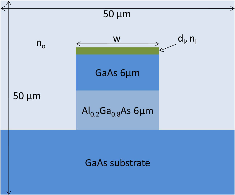
The basic optical structure studied herein comprises a GaAs/AlGaAs thin-film waveguide, as shown in Fig. 1. The refractive indices of GaAs and were fixed at 3.3 and 3.2, respectively. The thickness of the AlGaAs optical buffer layer and the actually waveguiding GaAs layer were fixed at 6 μm each, as this system was already experimentally studied [12,13]. Consequently, the waveguide width () was varied to optimize the sensitivity and the fraction of light propagating as an evanescent field for different wavelength ranges. The analytical sensitivity of such GaAs waveguides was calculated by varying either the refractive index of the outer medium () or by simulating an absorbing analyte layer with varying thickness () at a fixed refractive index () [19]. A dimensional cross section of the entire model (i.e., semiconductor structures and surrounding air) of was selected with at least 15 μm of bulk air surrounding the waveguide. Furthermore, a 20 μm GaAs substrate was modeled, thus ensuring a robust and constant model used during all simulated parameters reported herein. The computational model was meshed using a tetrahedral grid with a maximum element size of [20]. Thereafter, Maxwell’s equations were solved to determine the electric field distribution of transversal magnetic polarized radiation within a GaAs thin-film waveguide according to where is the electric field intensity (V/m), is the relative permittivity of the material, and is the free-space wavenumber.
Sign up for Photonics Research TOC. Get the latest issue of Photonics Research delivered right to you!Sign up now

Figure 1.Cross section of the simulation model () comprising a GaAs/AlGaAs waveguide with a 6 μm AlGaAs layer (optical buffer), a 6 μm GaAs layer (actual waveguide), and a 20 μm thick GaAs substrate. The width (), the thickness of the absorbed layer () simulating an analyte, and the refractive index of the outer medium () were varied during the simulations.
3. MODE ANALYSIS
In order to perform a comprehensive mode analysis, a cross section of a GaAs/AlGaAs waveguide structure (see Fig. 1) was used during simulations as a repetitive building block. The outer medium was selected as air with a refractive index of . Preliminary simulations revealed an early cutoff of the guided mode for widths at and multimode behavior for widths at . Below the cutoff, light may not propagate within the waveguide structure. In addition, no further signal improvement is expected above the multimode regime. Hence, calculations were performed individually for both spectral regions of interest using different simulation parameters for the waveguide width. Consequently, the waveguide width was varied from 3 to 8 μm for the wavelength regime at and from 8 to 20 μm for the wavelength regime at , respectively. A summary of the simulated modal behavior is illustrated in Fig. 2, where the effective refractive index () of the guided mode is plotted versus the waveguide width.

Figure 2.Dependence of the modal behavior on the width of the waveguide (A) for the amide region (), and (B) for the carbohydrate region (). (C) The fundamental guided mode of a 5 μm wide waveguide, and (D) the first-order mode of a 11 μm wide waveguide at a wavelength at are also illustrated.
The cutoff represents the region where light may not propagate within the waveguide, and only a leaky mode is present as a consequence of the waveguide dimensions (i.e., in terms of geometric dimensions for supporting at least one guided mode). In the single-mode regime, the analytically most sensitive waveguide structure is anticipated as illustrated in Fig. 2.C for a 5 μm wide and 6 μm thick waveguide. By further increasing the waveguide width at a constant thickness, first a second mode (Fig. 2.D), and later multiple modes appear, which results in lower analytical sensitivity, as the energy of the evanescent field is distributed among several light modes. In addition, leakage into the substrate (Fig. 2.D), which is mainly an issue for longer wavelengths, has to be taken into account, as the overall light throughput of the waveguide structure may be, accordingly, significantly reduced. The simulations executed in the present study revealed that single-mode waveguiding is ensured for a waveguide width of 4–7 μm at and of 10–16 μm at .
The effective refractive index of a waveguide can be either varied by changing the absolute refractive index in the sensing area (i.e., bulk sensitivity) or by adapting the thickness of an adjacent absorbing analyte layer (i.e., surface sensitivity) following
Both options for modulating the sensitivity were calculated, thus facilitating an estimation on their influence on the effective refractive index and, hence, for determining the optimal waveguide width (i.e., providing the highest analytical sensitivity).
Surface sensitivity () has been defined as the variation of the effective refractive index () with respect to the variation of the thickness of an absorbing layer () within the sensing volume at a fixed refractive index. For these considerations, the refractive index of the absorbed layer was fixed at 1.3, which is a reasonable approximation for most solid and liquid samples. The thickness of that layer was subsequently increased from 1 to 2000 nm, and the corresponding effective refractive index was calculated and plotted against the thickness of the absorbing analyte layer (Fig. 3). The exponential correlation between the thickness of the absorbed layer and the effective refractive index fit well to the exponential decay of the intensity of the evanescent field.

Figure 3.Exponential fit of the effective refractive index of a 13 μm wide waveguide at a wavelength at as a function of the absorbing analyte layer thickness.
The obtained data points for versus have been fitted with a first-order exponential function according to
After Taylor expansion, the quantity provides a value for the surface sensitivity in the linear region. As expected, the surface sensitivity increases with decreasing waveguide width, as a larger fraction of the propagating mode is forced toward the waveguide/sample interface leading to an increased evanescent field. In turn, the maximum surface sensitivity was evident for a 5 μm wide waveguide at and for a 13 μm wide structure at . Although smaller waveguide widths (i.e., ) are still single-mode, it appears that leakage into the substrate superimposes the gain resulting from a reduction of the waveguide width, thus providing an overall lower surface sensitivity.
The bulk sensitivity of such devices is defined as the variation of the effective refractive index () with respect to a variation of the absolute refractive index within the sensing volume (). Hence, the refractive index was varied from 1.0 to 1.3, and the effective refractive index was calculated for each waveguide width. As shown in Fig. 4, the bulk sensitivity has then been evaluated as the slope of versus (i.e., following a linear relationship). Then, the calculated slopes were plotted versus the waveguide width to determine the maximum of the bulk sensitivity. Again, it was evident that a narrower waveguide will increase the sensitivity of the device. Finally, the relationship between the evanescent field intensity in the sensing area and the width of the waveguide was determined, and the mode profiles of the individual (i.e., single) modes were calculated. The normalized electric field component was then plotted along a perpendicular line through the middle of the waveguide, as shown in Fig. 5 (red line).

Figure 4.Linear fit of the effective refractive index of a 5 μm wide waveguide at a wavelength at as a function of the refractive index of the outer medium.

Figure 5.(Top) Normalized electric field component along the center axis of a waveguide versus the waveguide width. Inset illustrates the waveguide section of the simulated electric field for a 5 μm wide waveguide at . (Bottom) Magnified view of the electric field above the waveguide surface (i.e., the evanescent field).
The fraction of the electric field component above the waveguide structure was calculated by integrating the normalized electric field, thus providing the energy within the evanescent field. Evidently, narrowing the waveguide width results in an increased fraction of energy above the waveguide. Hence, the increased sensitivity for narrow waveguides is a direct consequence of the increased intensity of the electric field emanating from the waveguide surface. However, reducing the width of the waveguide may also increase the fraction of light leaking into the substrate, as shown in Fig. 5 for a 4 μm wide waveguide.
4. CONCLUSIONS
Simulations were performed for semiconductor GaAs/AlGaAs thin-film waveguides, thus determining optimal waveguide geometries for two wavelength regimes relevant to chem/bio sensing applications of such structures. The most sensitive waveguide structure for the amide region was found at a width of 5 μm, while 13 μm appears most suitable for the carbohydrate region, respectively. Optimizing MIR thin-film waveguides for analytical applications requires that the longest wavelength of interest is considered in order to provide sufficient optical throughput within the desired wavelength regime. The achievable sensitivity of thin-film waveguides is a key parameter for analytical strategies aiming at label-free detection of minute quantities of biomolecules such as proteins, DNA, etc. Consequently, optimization of the waveguide structure toward higher sensitivities is crucial for MIR chem/bio sensing and assay platforms. Simulations of frequency-matched thin-film waveguides may furthermore facilitate design and development of sophisticated on-chip resonator and interferometer systems with superior sensitivity taking advantage of the inherent molecular selectivity provided by MIR radiation.
ACKNOWLEDGMENT
Acknowledgment. The research leading to these results has received funding from the European Union’s Seventh Framework Programme managed by REA Research Executive Agency http://ec.europa.eu/rea (FP7/2007-2013) under grant agreement no. 314018 FP7-SME-2012-SME. The authors gratefully acknowledge support of this study by the Kompetenznetz Funktionelle Nanostrukturen Baden Wuerttemberg, Germany.
References
[1] B. Mizaikoff. Waveguide-enhanced mid-infrared chem/bio sensors. Chem. Soc. Rev., 42, 8683-8699(2013).
[2] R. F. Kazarinov, R. A. Suris. Possible amplification of electromagnetic waves in a semiconductor with a superlattice. Fiz. Tekh. Poluprovodn., 5, 797-800(1971).
[3] J. Faist, F. Capasso, D. L. Sivco, C. Sirtori, A. L. Hutchinson, A. Y. Cho. Quantum cascade laser. Science, 264, 553-556(1994).
[4] R. Q. Yang. Infrared laser based on intersubband transitions in quantum well. Superlattices Microstruct., 17, 77-83(1995).
[5] C. H. Lin, R. Q. Yang, D. Zhang, S. J. Murry, S. S. Pei, A. A. Allerman, S. R. Kurtz. Type-II interband quantum cascade laser at 3.8 μm. Electron. Lett., 33, 598-599(1997).
[6] B. E. A. Saleh, B. E. A. Saleh, M. C. Teich, M. C. Teich. Semiconductor photon sources. Fundamentals of Photonics, 644-673(2007).
[7] F. Capasso, C. Gmachl, D. L. Sivco, A. Y. Cho. Quantum cascade lasers. Phys. Today, 55, 34-40(2002).
[8] J. Z. Chen, Z. Liu, C. Gmachl, D. Sivco. Silver halide fiber-based evanescent-wave liquid droplet sensing with room temperature mid-infrared quantum cascade lasers. Opt. Express, 13, 5953-5960(2005).
[9] C. Charlton, A. Katzir, B. Mizaikoff. Infrared evanescent field sensing with quantum cascade lasers and planar silver halide waveguides. Anal. Chem., 77, 4398-4403(2005).
[10] S. MacDonald, K. Michel, D. LeCoq, C. Boussard-Pledel, B. Bureau. Optical analysis of infrared spectra recorded with tapered chalcogenide glass fibers. Opt. Mater., 25, 171-178(2004).
[11] T. Lewi, A. Katzir. Silver halide single-mode strip waveguide for the mid-infrared. Opt. Lett., 37, 2733-2735(2012).
[12] C. Charlton, M. Giovannini, J. Faist, B. Mizaikoff. Fabrication and characterization of molecular beam epitaxy grown thin-film GaAs waveguides for mid-infrared evanescent field chemical sensing. Anal. Chem., 78, 4224-4227(2006).
[13] M. Sieger, F. Balluff, X. Wang, S.-S. Kim, L. Leidner, G. Gauglitz, B. Mizaikoff. On-chip integrated mid-Infrared GaAs/AlGaAs Mach-Zehnder interferometer. Anal. Chem., 85, 3050-3052(2013).
[14] N. Hô, M. C. Phillips, H. Qiao, P. J. Allen, K. Krishnaswami, B. J. Riley, T. L. Myers, N. C. Anheier. Single-mode low-loss chalcogenide glass waveguides for the mid-infrared. Opt. Lett., 31, 1860-1862(2006).
[15] C. Vigreux, E. Barthélémy, L. Bastard, J. Broquin, M. Barillot, S. Ménard, G. Parent, A. Pradel. Realization of single-mode telluride rib waveguides for mid-IR applications between 10 and 20 μm. Opt. Lett., 36, 2922-2924(2011).
[16] X. Wang, S.-S. Kim, R. Rossbach, M. Jetter, P. Michler, B. Mizaikoff. Ultra-sensitive mid-infrared evanescent field sensors combining thin-film strip waveguides with quantum cascade lasers. Analyst, 137, 2322-2327(2012).
[17] G. Kos, H. Lohinger, R. Krska. Fourier transform mid-infrared spectroscopy with attenuated total reflection (FT-IR/ATR) as a tool for the detection of Fusarium fungi on maize. Vib. Spectrosc., 29, 115-119(2002).
[18] D. McMullin, B. Mizaikoff, R. Krska. Advancements in the determination of fungal derived contaminations in food crops by IR spectroscopic approaches. Anal. Bioanal. Chem., 407, 653-660(2015).
[19] F. Prieto, B. Sepúlveda, A. Calle, A. Llobera, C. Domínguez, A. Abad, A. Montoya, L. M. Lechuga. An integrated optical interferometric nanodevice based on silicon technology for biosensor applications. Nanotechnology, 14, 907-912(2003).
[20] G. Veronis, S. Fan. Theoretical investigation of compact couplers between dielectric slab waveguides and two-dimensional metal-dielectric-metal plasmonic waveguides. Opt. Express, 15, 1211-1221(2007).

![]()
![]()
![]()
![]()


