• Photonics Research
  • Vol. 2, Issue 3, A19 (2014)
Takanori Shimizu1、2、*, Nobuaki Hatori1、2, Makoto Okano1、3, Masashige Ishizaka1、2, Yutaka Urino1、2, Tsuyoshi Yamamoto1、2, Masahiko Mori1、3, Takahiro Nakamura1、2, and and Yashuhiko Arakawa4
Author Affiliations
  • 1Institute for Photonics-Electronics Convergence System Technology (PECST), Japan
  • 2Photonics Electronics Technology Research Association (PETRA), West 7SCR, 16-1 Onogawa, Tsukuba, Ibaraki 305-8569, Japan
  • 3National Institute of Advanced Industrial Science and Technology (AIST), West 7SCR, 16-1 Onogawa, Tsukuba, Ibaraki 305-8569, Japan
  • 4Institute of Industrial Science, The University of Tokyo, 4-6-1 Komaba, Meguro, Tokyo 153-8505, Japan
  • show less
    DOI: 10.1364/PRJ.2.000A19 Cite this Article Set citation alerts
    Takanori Shimizu, Nobuaki Hatori, Makoto Okano, Masashige Ishizaka, Yutaka Urino, Tsuyoshi Yamamoto, Masahiko Mori, Takahiro Nakamura, and Yashuhiko Arakawa, "Multichannel and high-density hybrid integrated light source with a laser diode array on a silicon optical waveguide platform for interchip optical interconnection," Photonics Res. 2, A19 (2014) Copy Citation Text show less

    Abstract

    A hybrid integrated light source was developed with a configuration in which a laser diode (LD) array was mounted on a silicon optical waveguide platform for interchip optical interconnection. This integrated light source is composed of 13-channel stripes with a pitch of 20 or 30 μm. The output power of each LD in the 400 or 600-μm long LD array was over 40 mW at room temperature without cooling. An output power uniformity was 1.3 dB including an LD array power uniformity. The use of a SiON waveguide with a spot size converter resulted in an optical coupling loss of 1 dB between an LD and SiON waveguide. The integrated light source including 52 output ports demonstrated a reduction in the footprint per channel. We also demonstrated a light source with over 100 output ports in which the number of output ports is increased by using a waveguide splitter and multichip bonding. These integrated light sources are practical candidates for use with photonic integrated circuits for high-density optical interconnection.

    1. INTRODUCTION

    An optical interconnect with silicon photonics is thought to be a promising solution to the problem of bandwidth bottleneck in LSI chips [1] because of the intrinsic properties of optical signals, including wide bandwidth, low latency, low power consumption, and low mutual interference and the compatibility with CMOS process technology. For interchip interconnects, we proposed a “photonics-electronics convergence system” [24]. A light source, optical modulators, and photodetectors (PDs) are integrated on a single silicon substrate and are optically linked to each other via silicon waveguides. LSI bare chips are mounted on the substrate and are electrically connected to the optical modulators and PDs. By using this system, the function of electrical wiring on a conventional printed circuit board (PCB) can be achieved with an optical interconnect on a silicon substrate, which is an area that is 1/100 of a PCB. The target bandwidth density of the system is 10Tbit/s at 1cm2.

    In this system, the integrated CW light source must be multichannel, high density, and high power. Although integrated light sources formed on silicon-on-insulator (SOI) substrates have previously been reported [58], they have some challenges that need to be resolved for practical use, primarily optical output power and its efficiency. A hybrid integration of a light source with a laser diode (LD) on a silicon optical waveguide platform is preferable, because the optical output power of the LD is relatively high, the LD and the silicon optical waveguide platform can be individually optimized, and LD mounting technology is well-developed in silica waveguide-based platforms [9,10]. However, the pitch of a conventional hybrid integrated light source was fabricated for an optical fiber array whose pitch was 250 μm [11] and size was large for an interchip interconnection.

    We demonstrated a hybrid integrated light source with a configuration in which an LD array is mounted on a silicon optical waveguide platform for interchip optical interconnection [12]. We also demonstrated a light source with over 100 output ports in which the number of output ports is increased by using a waveguide splitter and multichip bonding [13,14].

    In this paper, we discuss our multichannel and high density hybrid integrated light source. The paper is organized as follows. In Section 2, we describe the concept of the multichannel and high-density hybrid integrated light source to approach a bandwidth of 10Tbit/s considering the system requirements. In Section 3, we present a LD array structure, silicon waveguide platform structure and fabrication, and hybrid integration technology in detail. The optical characteristics of a 13 channel light source are shown in Section 4 as the main structure of the light source. We show reducing the footprint per channel by introducing a waveguide splitter, describe the details of the multichip bonding technology to increase the number of output ports, and discuss the output power variation from the over 100 output ports of the light source in Section 5. Then, the summary is given in Section 6.

    2. CONCEPT OF INTEGRATED LIGHT SOURCE

    The integrated light source in the photonics-electronics convergence system is shown in Fig. 1, and the system requirements of the light source are listed in Table 1. For a high-density light source, a narrow pitch and small footprint per channel are required. An overall port number of light source is defined by the channel number of a laser, the number of lasers, and the splitting number of the waveguide splitter. For a high-power light source, a high laser power and low coupling loss are required. To reach a bandwidth of 10Tbit/s, an over 1000-ch output port is needed, assuming 10Gbit/s for each port. For example, each channel of the integrated light source consists of a 1×4 splitter, 20 lasers, and 13-channel laser array. Therefore, the system requirements of the light source were defined, as listed in Table 1. The laser array number of 13 is intended to be a redundant output port number in order to exceed 100 or 1000 output ports with splitters and lasers.
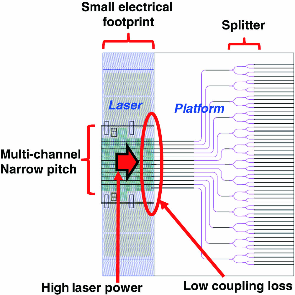
    Schematic of integrated light source in photonics-electronics convergence system.

    Figure 1.Schematic of integrated light source in photonics-electronics convergence system.

    RequirementsTarget
    High densityNarrow pitch<1/10 conventional laser array
    Small footprint/ch<0.01mm2/ch
    MultichannelMultichannel/chip13 ch
    Multi-chip10–20 chip
    splitter1×4, 1×8
    High powerHigh laser power>10mW/ch
    Low coupling loss2–3 dB

    Table 1. Requirements of Integrated Light Source for 10Tbit/s Optical Interconnects

    3. STRUCTURE DESIGN AND FABRICATION

    To meet these system requirements, a hybrid integrated light source with an LD array on a silicon waveguide platform was developed. The main structure is shown in Fig. 2 [12]. We describe a LD array structure, a silicon waveguide platform structure and fabrication, and a hybrid integration technology.

    Hybrid integration structure with an LD array on a silicon waveguide platform.

    Figure 2.Hybrid integration structure with an LD array on a silicon waveguide platform.

    A. LD Structure

    Each LD in the array is a Fabry–Perot type LD with a spot size converter (SSC) including an inverse taper at the waveguide facet side and has a structure consisting of an InGaAsP base strained multiquantum well buried heterostructure (lasing wavelength of about 1.55 μm). The LD array has 13-channel stripes at a pitch of about 20 or 30 μm and alignment marks, as shown in Fig. 3. The stripe pitch can be drastically narrowed by using a single electrode, unlike the conventional LD array. The operation current is injected into these stripes through a single electrode, and the LD array emits 13-channel optical outputs simultaneously.

    Photograph of 13-channel LD array. Cavity length is 400 μm, and array pitch is 30 μm.

    Figure 3.Photograph of 13-channel LD array. Cavity length is 400 μm, and array pitch is 30 μm.

    B. Silicon Waveguide Platform Structure and Fabrication

    The platform consists of waveguides with SSCs and an LD mounting stage. At the SSC, SiON and silicon optical waveguides are connected with a SiON core surrounding an inversely tapered silicon tip. The silicon optical waveguides have a core section size 440 nm wide and 220 nm high, and the SiON waveguides have a core section size of 2.5μm×2.5μm. The tip width and length of the tapered waveguide are 100 nm and 200 μm, respectively. The silicon and SiON waveguides include a 2 or 3 μm thick upper cladding layer and a 3-μm-thick lower cladding layer. The core layer and lower cladding correspond to the silicon on insulator (SOI) layer and the buried oxide (BOX) layer on the SOI substrate, respectively. The SiON waveguide facet was fabricated and the BOX layer removed from the mounting area by dry etching. The silicon alignment marks and silicon pedestals were also formed by dry etching. A thin film SiO2 insulating layer was deposited on a silicon substrate. An electrode was then formed on the mounting stage.

    The fabrication technology was based on a previous report [15], but the array waveguide was fabricated between two alignment marks. Figure 4 shows a scanning electron microscope image of the waveguide facet made by dry etching. The angle of the facet measured about 85 degrees.

    Scanning electron microscope image of waveguide facet made by dry etching.

    Figure 4.Scanning electron microscope image of waveguide facet made by dry etching.

    C. Hybrid Integration

    The LD array is mounted on the silicon optical waveguide platform with AuSn solder bumps by flip-chip bonding, as shown in Fig. 5(a). We adapted the visual alignment between the alignment marks on the LD array and the mounting stage by infrared transmission light to the LD flip-chip bonding technology for horizontal positioning. This passive alignment technology was adapted to the optical transceivers with a silica [9] or polymer [16,17] platform and the wavelength tunable lasers with a silica [10] and silicon [15] based platform. The standard deviation of the horizontal alignment accuracy of the LD chip mounter was 0.21 μm [10], (the accuracy is better than ±0.5μm). The vertical alignment of the LD array was precisely adjusted by the positioning of the top surface of the silicon pedestal including the insulting layer. The vertical alignment accuracy was made better than ±0.1μm by dry etching and deposition controllability. Thus, multichannel alignment was simultaneously achieved, as shown in Fig. 5(b).

    (a) Schematic of LD mounting structure and (b) LD mounting image focused on alignment marks by transmission infrared light.

    Figure 5.(a) Schematic of LD mounting structure and (b) LD mounting image focused on alignment marks by transmission infrared light.

    4. THIRTEEN-CHANNEL INTEGRATED LIGHT SOURCE AND ITS OPTICAL CHARACTERISTICS

    A 13-channel light source was fabricated on the basis of the structure design. The fabricated hybrid integrated light source is shown in Fig. 6. The length and width of the 13-channel LD array were 600 μm each. To avoid noncoupling light from the LD array, silicon optical waveguides were formed in an S-shape crank, and output ports were shifted. The waveguide pitch was 30 μm, the same as the LD array. The platform size was 1450μm×1670μm. We describe a optical characteristics of the 13-channel LD array itself, an optical coupling tolerance between a LD and a SiON waveguide, and an output uniformity of the light source.

    (a) Schematic and (b) photograph of 13-channel hybrid integrated light source.

    Figure 6.(a) Schematic and (b) photograph of 13-channel hybrid integrated light source.

    A. LD Performance

    Figure 7 shows the dependence of the total output power of the 13-channel LD array on the operation current at room temperature without cooling. Since the operation current was injected into 13 stripes through a single electrode, the threshold current was 158 mA, and the total power was 525 mW at 2 A. The total output power and the total threshold current of the 13-channel LD array were 13 times those of a single-channel LD. Therefore, the output power of each LD in the LD array was over 40 mW. By using the thermal analysis of a laser source [6], the thermal interference between each channel in the LD array was estimated at the total current of 2A. The temperature increase around the central channel was 25°C, which was slightly higher than the temperature increase of 22°C at the outer channels because of the heat generated from both sides. However, in spite of the temperature increase in the LD array, high power operation in each LD was achieved.

    Dependence of light output of 13-channel LD array on operating current at room temperature without cooling.

    Figure 7.Dependence of light output of 13-channel LD array on operating current at room temperature without cooling.

    B. Optical Coupling Tolerance

    The optical coupling tolerance between the LD and the SiON waveguide along the horizontal and vertical directions was measured, as shown in Fig. 8. The spot sizes of the LD stripe were 3.5 μm in the horizontal direction and 3.8 μm in the vertical direction. The spot sizes of the SiON waveguide were 3.0 μm in the horizontal direction and 4.0 μm in the vertical direction. The optical coupling loss was 1 dB at zero deviation. The tolerances of the 1-dB down coupling loss were ±0.9μm in the horizontal direction and ±1.1μm in the vertical direction. These values are sufficiently wide compared with the horizontal and vertical alignment accuracy described in Section 3.

    Optical coupling tolerance between LD and SiON waveguide along horizontal and vertical directions.

    Figure 8.Optical coupling tolerance between LD and SiON waveguide along horizontal and vertical directions.

    C. Output Uniformity

    The relative light intensity of the 13-channel LD array and waveguide output ports in the light source are shown in Fig. 9. The output power uniformity across the output ports was better than 1.3 dB, while the output power uniformity across the LD array was better than 0.7 dB. This excellent uniformity is a result of the precise alignment accuracy of the flip-chip bonding technology.

    Relative light intensity of 13-channel LD array and waveguide output ports on integrated light source.

    Figure 9.Relative light intensity of 13-channel LD array and waveguide output ports on integrated light source.

    5. HIGH DENSITY AND MULTICHANNEL HYBRID INTEGRATED LIGHT SOURCE

    A. Reducing Footprint per Channel by Introducing Waveguide Splitter

    The bandwidth density of the photonic integrated circuits depends on the footprint per channel of the optical components [24]. The footprint of the light source can be reduced by introducing a waveguide splitter. We fabricated a light source including 52 output ports, in which the silicon optical waveguides are split in four by double cascade 1×2 multimode interferometer (MMI) splitters, as shown in Fig. 10. The 13-channel LD array was 600 μm wide and 400 μm long. The size of the light source was 1650μm×1450μm, and the electrode size was 1060μm×380μm. The footprint per channel was 0.008mm2.

    (a) Schematic and (b) photograph of integrated light source with 52 output ports made possible by introducing waveguide splitter.

    Figure 10.(a) Schematic and (b) photograph of integrated light source with 52 output ports made possible by introducing waveguide splitter.

    B. Increasing Number of Output Ports with Multichip Bonding Technology

    The number of output ports was increased by using waveguide splitters and multichip bonding [13,14]. Multiple LD array chips were mounted on a single substrate with flip-chip bonding technology, as shown in Fig. 11(a). The LD array is mounted with AuSn solder bumps by flip-chip bonding described in Section 3.

    Schematic showing multichip bonding technology. (a) Mounting structure and (b) illustration of diffusion of Au on surface of electrodes into AuSn bump at soldering.

    Figure 11.Schematic showing multichip bonding technology. (a) Mounting structure and (b) illustration of diffusion of Au on surface of electrodes into AuSn bump at soldering.

    The Au composition of the AuSn solder we used is 80 wt. %. This composition is eutectic composition and the melting point is 280°C. When the Au content is over 80 wt. %, the melting point of AuSn increases dramatically, as shown in the phase diagram of AuSn alloy [18]. Once the first LD chip is mounted on the stage at operation temperature (T0), the composition of Au in the AuSn bumps increases due to the diffusion of Au on the surface of the electrodes, as shown in Fig. 11(b), and the melting point of the bumps (T1) becomes higher (T1>T0). Therefore, the position of the first LD does not deviate from the bonding position on this stage when the second LD chip is mounted at the same temperature as that of the first bonding (T0).

    By using a waveguide splitter and this multichip bonding, we fabricated a light source with 104 output ports in which the silicon optical waveguides are split in four by double cascade 1×2 MMI splitters and two LD array chips are mounted on a silicon waveguide platform, as shown in Fig. 12. The LD array chip was 600 μm wide and 400 μm long. The pitches of LD array 1 and 2 were 30 and 20 μm, respectively. The size of the light source was 3220μm×1450μm.

    (a) Schematic and (b) photograph of integrated light source with 104 output ports with two LD array chips.

    Figure 12.(a) Schematic and (b) photograph of integrated light source with 104 output ports with two LD array chips.

    Figure 13 shows the near-field pattern of the light source at an operation current of 450 mA for each chip. All 104 optical outputs were observed. The light source with over 100 output ports corresponds to a 1Tbit/s transmitter, assuming 10Gbit/s for each port.

    Near-field pattern of outputs in integrated light source with 104 output ports.

    Figure 13.Near-field pattern of outputs in integrated light source with 104 output ports.

    Figure 14 shows a histogram of the relative intensity of the 104 output ports, which is taken at a current of 450 mA for each LD chip. A histogram of 1st–52nd channel port with the first LD array is shown in Fig. 14(a), and the standard deviation was 0.80 dB. A histogram of 53rd–104th channel port with the second LD array is shown in Fig. 14(b), and the standard deviation was 0.64 dB. The output power variation at a LD array was due to the waveguide loss depending on the fan-out length variation and fabrication nonhomogeneity.

    Histogram of relative intensity of output ports. (a) 1st–52nd channel port and (b) 53rd–104th channel port.

    Figure 14.Histogram of relative intensity of output ports. (a) 1st–52nd channel port and (b) 53rd–104th channel port.

    These results show that multichannel, high density, and high power operation can be demonstrated with a hybrid integrated light source with an LD array on a silicon optical waveguide platform.

    6. CONCLUSION

    We developed a hybrid integrated light source with a configuration in which an LD array was mounted on a silicon optical waveguide platform for interchip optical interconnection. Experimental results demonstrated a high density (20- or 30-μm pitch) and 13-channel uniform operation with the integrated light source as well as a low loss coupling due to the SiON waveguides with SSCs (coupling loss of 1 dB at zero deviation). The integrated light source including 52 output ports demonstrated a reduction in the footprint per channel. We also demonstrated a light source with more than 100 output ports in which the number of output ports was increased by using a waveguide splitter and multichip bonding. We expect the multichannel, high-density hybrid integrated light source to be easily adapted to the photonics-electronics convergence system for interchip interconnection.

    References

    [1] I. A. Young, E. Mohammed, J. T. S. Liao, A. M. Kern, S. Palermo, B. A. Block, M. R. Reshotko, P. L. D. Chang. Optical I/O technology for tera-scale computing. IEEE J. Solid-State Circuits, 45, 235-248(2010).

    [2] Y. Urino, T. Shimizu, M. Okano, N. Hatori, M. Ishizaka, T. Yamamoto, T. Baba, T. Akagawa, S. Akiyama, T. Usuki, D. Okamoto, M. Miura, M. Noguchi, J. Fujikata, D. Shimura, H. Okayama, T. Tsuchizawa, T. Watanabe, K. Yamada, S. Itabashi, E. Saito, T. Nakamura, Y. Arakawa. First demonstration of high density optical interconnects integrated with lasers, optical modulators, and photodetectors on single silicon substrate. Opt. Express, 19, B159-B165(2011).

    [3] Y. Urino, Y. Noguchi, M. Noguchi, M. Imai, M. Yamagishi, S. Saitou, N. Hirayama, M. Takahashi, H. Takahashi, E. Saito, M. Okano, T. Shimizu, N. Hatori, M. Ishizaka, T. Yamamoto, T. Baba, T. Akagawa, S. Akiyama, T. Usuki, D. Okamoto, M. Miura, J. Fujikata, D. Shimura, H. Okayama, H. Yaegashi, T. Tsuchizawa, K. Yamada, M. Mori, T. Horikawa, T. Nakamura, Y. Arakawa. Demonstration of 12.5-Gbps optical interconnects integrated with lasers, optical splitters, optical modulators and photodetectors on a single silicon substrate. Opt. Express, 20, B256-B263(2012).

    [4] Y. Urino, S. Akiyama, T. Akagawa, T. Baba, T. Usuki, D. Okamoto, M. Miura, J. Fujikata, T. Shimizu, M. Okano, N. Hatori, M. Ishizaka, T. Yamamoto, H. Takahashi, Y. Noguchi, M. Noguchi, M. Imai, M. Yamagishi, S. Saitou, N. Hirayama, M. Takahashi, E. Saito, D. Shimura, H. Okayama, Y. Onawa, H. Yaegashi, H. Nishi, H. Fukuda, K. Yamada, M. Mori, T. Horikawa, T. Nakamura, Y. Arakawa. Demonstration of 30-Tbps/cm2 bandwidth density by silicon optical interposers fully integrated with optical components. 39th European Conference and Exhibition on Optical Communication, Mo.4.B.2(2013).

    [5] J. Liu, X. Sun, R.-C. Aguilera, Y. Cai, L. C. Kimerling, J. Michel. Monolithic Ge-on-Si lasers for integrated photonics. Proceedings of IEEE 7th International Conference on Group IV Photonics, 1-3(2010).

    [6] M. N. Sysak, H. Park, A. W. Fang, J. E. Bowers, R. Jones, O. Cohen, O. Raday, M. Paniccia. Experimental and theoretical analysis of a hybrid silicon evanescent laser. Opt. Express, 15, 15041-15046(2007).

    [7] K. Tanabe, K. Watanabe, S. Faure, Y. Arakawa. 1.3  μm InAs/GaAs quantum dot lasers on Si substrates with current injection across direct-bonded GaAs/Si heterostructures. 37th European Conference and Exhibition on Optical Communication, Tu.6.LeSaleve.1(2011).

    [8] S. Saito. Silicon and germanium quantum well light-emitting diode. Proceeding of IEEE 8th International Conference on Group IV Photonics, 166-168(2011).

    [9] N. Kimura, K. Shinozaki, N. Kitamura, Y. Fukutomi, Y. Minota, H. Tanaka, A. Sato, H. Ando. Receptacle transceiver module using silica waveguide for bi-directional transmission over single fiber. Proceeding of 53th Electronic Components and Technology Conference, 290-295(2003).

    [10] T. Takeuchi, M. Takahashi, K. Suzuki, S. Watanabe, H. Yamazaki. Wavelength tunable laser with silica-waveguide ring resonators. IEICE Trans. Electron., E92-C, 198-204(2009).

    [11] M. Shishikura, T. Ban, H. Ichikawa, T. Ido, M. Takahashi, K. Nakahara, E. Nomoto, Y. Matsuoka, K. Ishikawa, K. Ito, R. Takeyari, H. Sano, T. Hirose, H. Takahashi, T. Nagara, H. Chiba, S. Irikura. 10  Gbit/s per channel parallel optical transmitter and receiver modules for high-capacity interconnects. Proceeding of 53th Electronic Components and Technology Conference, 1040-1045(2003).

    [12] T. Shimizu, N. Hatori, M. Okano, M. Ishizaka, Y. Urino, T. Yamamoto, M. Mori, T. Nakamura, Y. Arakawa. High density hybrid integrated light source with a laser diode array on a silicon optical waveguide platform for inter-chip optical interconnection. Proceeding of IEEE 8th International Conference on Group IV Photonics, 181-183(2011).

    [13] T. Shimizu, N. Hatori, M. Okano, M. Ishizaka, Y. Urino, T. Yamamoto, M. Mori, T. Nakamura, Y. Arakawa. High density hybridly integrated light source with a laser diode array on a silicon optical waveguide platform. Integrated Photonic Research, Silicon and Nano Photonics, ITu4B.5(2012).

    [14] T. Shimizu, M. Okano, N. Hatori, M. Ishizaka, Y. Urino, T. Yamamoto, M. Mori, T. Nakamura, Y. Arakawa. Multi-channnel and high density hybrid integrated light source on a silicon optical waveguide platform. Asia Communications and Photonics Conference, AF3B.2(2012).

    [15] N. Fujioka, T. Chu, M. Ishizaka. Compact and low power consumption hybrid integrated wavelength tunable laser module using silicon waveguide resonators. J. Lightw. Technol., 28, 3115-3120(2010).

    [16] T. Shimizu, Y. Akimoto, K. Kurata. An opto-electronic hybrid integrated platform with a polymer optical waveguide for high performance and low cost modules. Proceeding of 54th Electronic Components and Technology Conference, 1042-1045(2004).

    [17] T. Sugimoto, T. Shimizu, Y. Akimoto, M. Noguchi, J. Sone, T. Watanabe, Y. Urino. A small and low cost bidirectional transceiver module with polymer waveguide for G-PON/Ge-PON. Proceeding of 57th Electronic Components and Technology Conference, 707-711(2007).

    [18] J. Ciulik, M. R. Notis. The Au-Sn phase diagram. J. Alloys Compd., 191, 71-78(1993).

    Takanori Shimizu, Nobuaki Hatori, Makoto Okano, Masashige Ishizaka, Yutaka Urino, Tsuyoshi Yamamoto, Masahiko Mori, Takahiro Nakamura, and Yashuhiko Arakawa, "Multichannel and high-density hybrid integrated light source with a laser diode array on a silicon optical waveguide platform for interchip optical interconnection," Photonics Res. 2, A19 (2014)
    Download Citation