
Zhiqiang WANG, Ji’an WU, Kunfeng CHEN, Dongfeng XUE. Large-size Er,Yb:YAG Single Crystal: Growth and Performance [J]. Journal of Inorganic Materials, 2023, 38(3): 329
- Journal of Inorganic Materials
- Vol. 38, Issue 3, 329 (2023)
Abstract
Yttrium aluminium garnet (Y3Al5O12, YAG) is important host material for phosphors, scintillators, and solid state lasers[1⇓-3]. With the valence 4f electrons shield by 5s and 5p electron orbits, the rare earth ions in the solid state often emit in narrow and strong bands[4]. The rare earths of most interest for selective emitters are ytterbium (Yb), thulium (Tm), erbium (Er), holmium (Ho) and dysprosium (Dy). Rare earth doped YAG crystal have been used in photonic applications ranging from near infrared (IR) emitters to cathode ray phosphors and scintillators since Y3+ being vicariate with trivalent lanthanide ions[5]. Yb3+ ions can absorb the light between 900 and 1000 nm with energy transfer (ET) from 2F7/2 to 2F5/2 level. Then, the energy can be transferred to the 4I11/2 level of Er3+, leading to laser emission at 2.94 μm wavelength. Therefore, Er and Yb doped glass, ceramics, fiber and single crystal materials have been synthesized for studying up-conversion luminescence and active lasing performances[6⇓⇓⇓-10]. Er3+,Yb3+: YAG crystals of a diameter of about 25 mm and a length of 60 mm were obtained using Cz method[7]. It was reported that 8 inch (20.32 cm) Yb:YAG single crystal was grown by Cz method[8]. The Er3+/Yb3+ co-doped YAG fiber (about 3 mm in length and 0.8 mm in cross section diameter) have been grown by laser heated pedestal growth[9]. Recently, Er,Yb co-doped YAG single crystals (70 mm×150 mm×15 mm) was grown by a modified horizontal directional crystallization method in Ar+(CO, H2) atmosphere using Mo crucible[11]. The growth of larger size of Er,Yb co-doped YAG single-crystals was still in demand.
However, it is a challenge to grow bulk YAG single crystals with low defects. We have used the chemical bonding theory of single crystal growth quantitatively to describe the anisotropic bonding behaviors of constituent atoms during YAG crystallizing, and ϕ3 inch(1 inch=2.54 mm) YAG crystal were obtained[12-13]. In this work, we grew Er,Yb:YAG single crystal with a diameter of 80 mm and length of 230 mm with fast growth method. The structure, defect, optical and luminescence performances were studied.
1 Experimental
1.1 Er,Yb:YAG crystal growth
The Er,Yb:YAG polycrystals were synthesized with the powders of Er2O3 (99.999%), Yb2O3 (99.999%), Y2O3 (99.999%) and Al2O3 (99.999%) as raw materials. First, all ingredients were dried to remove residual moisture from the powder to ensure accurate weighing. The doping concentrations of Yb3+ and Er3+ were 0.05% and 0.15% (in mass), respectively. The four powders were mixed and blended in a mixer for 24 h to ensure that the ingredients were well mixed. The mixed powders were then packed into a mould and compacted. Finally, the pressed cylinders were transferred to a muffle furnace and sintered at 1100 ℃ for 12 h to form polycrystalline Er,Yb:YAG.
The growth of Er,Yb:YAG single crystal was carried out by the Cz method in a nitrogen atmosphere. The sintered polycrystalline Er,Yb:YAG was put into an iridium crucible equipped with an intermediate frequency induction heating system Cz furnace, heated until the polycrystalline material is completely melted and held for a period. The YAG in the <111> direction was used as the seed crystal and seeding was performed manually. A series of subsequent crystal growth processes were controlled by an automatic control system with the following specific growth parameters: a pulling rate of 2-4 mm·h-1 and rotation rate of 5-10 r/min[12].
1.2 Characterization
The crystal phase of single crystal Er,Yb:YAG were examined with X-ray diffraction (XRD, Rigaku, Smartlab 3kW). The elemental analysis of the Er,Yb:YAG crystal was characterized by Energy-dispersive X-ray spectroscopy (EDS, Oxford, Ultim Max 100) and glow discharge mass spectrometry (GDMS, AstruM, Nu Instrument). Raman spectra were excited using Raman spectrometer (Horiba, LabRAM HR Evolution) with a 325 nm laser. Etched Er,Yb:YAG wafers were performed by optical microscope (Nikon, LV150). The refractive index of Er,Yb:YAG wafer was measured by Prism Coupling device (Metricon, Model 2010). The optical absorption and PL spectra were determined by UV-Vis spectrophotometer (Metash, UV-9000) and fluorescence spectrometer (Edinburgh, FLS 1000), respectively.
2 Results and discussion
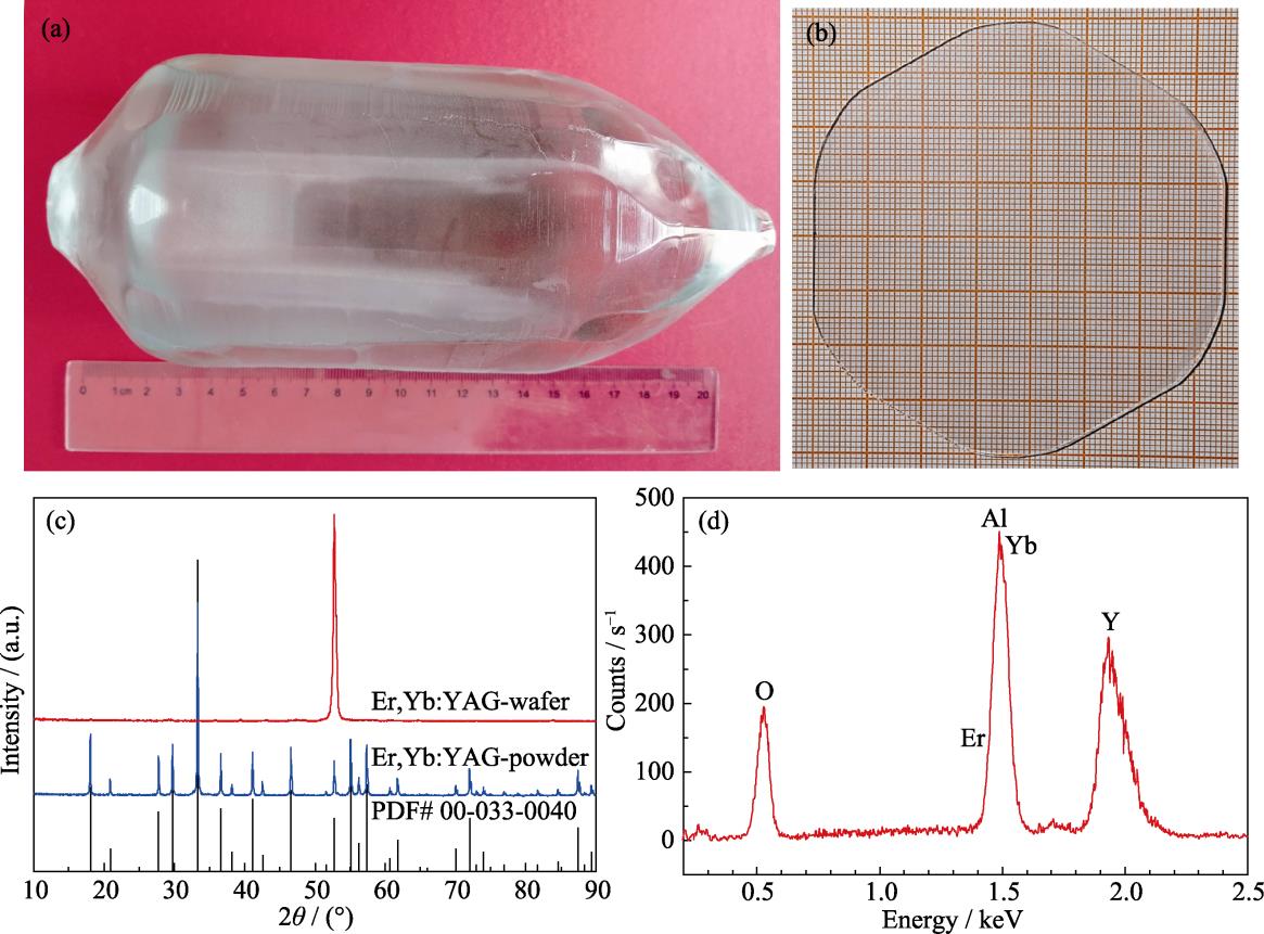
Fig. 1(a) shows the photograph of a large-size Er,Yb: YAG single crystal grown by the Cz method and annealed in air. Fig. 1(b) shows the picture of a wafer with a thickness of 1.5 mm cut perpendicular to the orientation of <111> and polished on both sides. The length and diameter of the crystal are 230 and 80 mm, respectively. The shape is characteristic of typical <111> orientation, and the crystal is colourless transparent and has no defects such as cracks and inclusions[14-15].
![]()
Figure 1.Characteristics of as-grown Er,Yb:YAG single crystal and wafer(a) With diameter of 80 mm and length of 230 mm; (b) Wafer with a thickness of 1.5 mm; (c) XRD patterns for wafer and ground powder; (d) EDS pattern of the wafer
Grind the annealed crystal into powder for XRD analysis, and the results are shown in Fig. 1(c). A comparison of the XRD results with the standard PDF cards (PDF# 00-033-0040) in the database shows that all peaks are well indexed to the cubic structure Y3Al5O12 (space group: $Ia\bar{3}d$), and no impurity phases are found, which means that the dopant ions are well substituted for the Y3+ lattice positions[16-17]. XRD tests on the YAG-doped wafer in Fig. 1(b) show only a sharp diffraction peak of the (444) crystal plane at 2θ=52.76o and no diffraction peaks of the other crystal planes, confirming its good quality.
The chemical compositions of Er,Yb:YAG crystal were determined by EDS and GDMS. It can be seen in Fig. 1(d) that Y, Al and O peaks are well detected. Because the element contents of Yb and Er are relatively low, and the characteristic energies of these elements are located at 1.521 and 1.405 keV, which are close to the peaks of Al (1.486 keV) and overlap, they cannot be distinguished well. GDMS is one of the effective means of analysing trace elements in conductors and semiconductors[18-19]. The actual doping concentrations of Er3+ and Yb3+ ions in YAG crystals were analysed using GDMS. The results showed that the actual doping content of Er3+ and Yb3+ was 0.13% and 0.049% (in mass), demonstrating the successful doping of Er3+ and Yb3+.
In order to study the defects present in the grown Er,Yb:YAG crystal, the polished wafers were chemically etched. The etching was carried out using concentrated phosphoric acid (H3PO4) at 180 ℃ for 60 min. A comparison of the wafer surface before and after corrosion is shown in Fig. 2. The corrosion pits are evenly distributed over the entire corrosion surface, and no dislocation corrosion pit features are observed, which means that the crystals are near-perfect[20-21].
![]()
Figure 2.Micrographs of wafer surface with (111) face(a, b) Before etching; (c, d) Etched in H3PO4 at 180 ℃ for 60 min
For cubic Y3Al5O12 (YAG) with space group $O_{h}^{10}-Ia\bar{3}d$, the irreducible representations as follows: Γ = 3A1g + 5A2g + 5A1u + 5A2u + 8Eg + 10Eu + 14T1g + 14T2g +18T1u + 16T2u. 25 modes are Raman active (3A1g, 8Eg and 14T2g) while 18 modes are IR active (18T1u)[22]. The Raman spectra of rare earth doped YAG have been recorded in the 100-1200 cm−1 spectral range at room temperature (Fig. 3 and Fig. 4(a)), which shows strong Raman bands at 259, 371, 402, 784 cm−1, medium bands at 161, 218, 548, 558, 692, 718, 859 cm−1, and weak bands at 294, 338, 754 cm−1. The low-frequency region (100-500 cm−1) can be attributed to the lattice vibrational mode and the translational motion of the RE3+(Y,Er,Yb), and also the mixing of translational, rotational and ν3 molecular mode of the [AlO4] unit. The intermediate- frequency region (500-600 cm−1) accounts to the ν2 molecular mode splitting of the [AlO4] unit while the high-frequency region (600-900 cm−1) can be assigned to the ν1 and ν4 internal modes of the tetrahedral [AlO4] unit[23-24]. According to the results of factor group analysis, the three A1g modes are related to the [AlO4] internal vibrations[25]. There is a weak Raman peak at 1100 cm−1, which may be the Yb-O vibration[26-27]. To investigate the doping uniformity of Er,Yb:YAG crystal grown by the Cz method, two sets of points were taken outside the center of the wafer (the inset of Fig. 4(b)). Raman spectra of these points showed that the peak intensity of the C4 point is the highest at the 783 cm−1 band. Raman spectra of other points are similar to those of C1, C2 and O3 (Fig. 4(a)). Lorentz fitting was performed on all selected points at the 783 cm−1 band (Fig. 4(b)).
![]()
Figure 3.Raman spectrum of Er,Yb:YAG
![]()
Figure 4.Raman spectra of different points at Er,Yb:YAG wafer(a) Five points on a straight line; (b) Peak positions and FWHM obtained by Lorentz fitting at the 783 cm-1 band with nisets showing Er,Yb:YAG wafer and schematic diagram of Raman test points
The peak position obtained by B5 point fitting is 784 cm−1, which means that B5 point is subjected to higher compressive stress than other points. The peak position varies from 781.5 to 784.1 cm−1, and FWHM varies from 20 to 22.2 cm−1. The peak position and FWHM of each point were not greatly changed. Therefore, it can be considered that the doping uniformity of the wafer is relatively acceptable.
The room-temperature UV-Vis absorption spectra in 200-1050 nm of Er,Yb:YAG in Fig. 1(b) are shown in Fig. 5. The absorption bands centered at 914 and 941 nm are attributed to the transitions from the ground state to the excited state (2F7/2→2F5/2) of Yb3+ ion[11,28 -29]. It can be seen from the illustration in Fig. 5 that Er,Yb:YAG crystal has strong UV absorption band when the wavelength less than 230 nm, which is caused by charge transfer (CT) luminescence from O2− to Yb3+[30-31]. Except for the optical absorption of Yb3+ and CT luminescence, all remaining peaks in the absorption spectra are attributed to the transitions of Er3+ ion[11,32]. The assignment of the absorption lines of the Er3+ ion is presented in Table 1. The refraction index of Er,Yb:YAG is 1.83.
![]()
Figure 5.Optical absorption spectra of Er,Yb:YAG crystal in the range of 200-1050 nm at room temperature
| Wavelength/nm | Assignment (from ground 4I15/2) |
|---|---|
| 255 | 4D7/2 |
| 356 | 2K15/2 |
| 364 | 2G9/2 |
| 381 | 4G11/2 |
| 407 | 2H9/2 |
| 442 | 4F3/2 |
| 450 | 4F5/2 |
| 488 | 4F7/2 |
| 518, 524 | 2H11/2 |
| 542 | 4S3/2 |
| 647, 655 | 4F9/2 |
| 788 | 4I9/2 |
| 961, 966 | 4I11/2 |
Table 1.
Correspondence between the experimentally observed absorption lines and energy levels of Er3+ in Er,Yb:YAG single crystal[11,33⇓⇓ -36]
Fig. 6 illustrates the emission spectra of crystals excited at different wavelengths at room temperature, 382 nm for Fig. 6(a) and 260 nm for Fig. 6(b). It can be seen from Fig. 6(a) that the green emission at 554 nm has the strongest emission peak, which corresponds to the 4S3/2→4I15/2 energy levels transition in Er3+ ion[37]. The violet emission at 405 nm shown in Fig. 6(b) is attributed to the 2H9/2→4I15/2 in Er3+ ion[38]. The decay curves of the fluorescence lifetimes of the emission peaks at 554 and 405 nm are presented in Fig. 6(c, d). The fitting results show that the fluorescence lifetimes are 17.92 and 52.09 μs, respectively.
![]()
Figure 6.Emission spectra of Er,Yb:YAG crystal at room temperature(a) Excited by 382 nm; (b) Excited by 260 nm; Fluorescent decay curves of (c) 554 nm; (d) 405 nm emission; Colorful figures are available on website
3 Conclusion
In this work, cubic-phase Er,Yb:Y3Al5O12 crystal with a diameter of 80 mm and length of 230 mm was obtained by the fast Cz growth method. Raman results of 17 points in cutting crystal wafer showed uniform peak number and position, which can be considered that the structure uniformity of the wafer is relatively acceptable. The refraction index of Er,Yb:YAG is 1.83. The absorption bands are attributed to the transitions from the ground state to the excited state of Yb3+ and Er3+ ions. Expect for the optical absorption of Yb3+ and CT luminescence, all remaining narrow peaks in the absorption spectra are attributed to the transitions of Er3+ ion. It is concluded that the fast growth method was effective for dual rare earth ions doping in YAG crystal.
References
[7] Z MIERCZYK, M KWASNY, K KOPCZYNSKI et al. Er3+ and Yb3+ doped active media for ‘Eye-Safe’ laser systems. Journal of Alloys and Compounds, 398(2020).
[8] G YANG, J HAN, X LI et al. Growth of 8 inch Yb:YAG single crystal by Czochralski method. Journal of Synthetic Crystals, 48:, 1216(2019).
[10] Y GUO, L HUANG, J ZHOU et al. Czochralski growth and investigation on the photoluminescence properties of YAG:Er single crystal. Journal of Synthetic Crystals, 48:, 24(2019).
[21] H B YIN, P Z DENG, F X GAN. Defects in YAG:Yb crystals. Journal of Applied Physics, 3825(1998).
[30] N GUERASSIMOVA, N GARNIER, C DUJARDIN et al. X-ray-excited charge transfer luminescence in YAG:Yb and YbAG. Journal of Luminescence, 94:, 11(2001).

Set citation alerts for the article
Please enter your email address
© Copyright 2018-2021 | Chinese Laser Press. All Rights Reserved 沪ICP备15018463号-20